IN3OTD's web site
...under perpetual construction.

Push-pull power amplifier with PD85004
I was needing a couple of low-distortion medium-power amplifier for increasing the maximum power output of the generators I use for IMD testing, so I built a couple of the PD85004 push-pull amplifiers described here, and in particular the lowest-distortion variant with center-tapped input transformer and gate-drain feedback. In a two-tone test this particular configuration can put out up to 6 W PEP while maintaining an output IMD3 better than -40 dBc.
Since these amplifiers will be used on the bench, I wanted to have a simple but robust enclosure (quite an exception for my circuits, which normally live as dead-bug style prototypes forever!); I find the tin boxes from Schubert a good and inexpensive solution for RF circuits, so the choice was easily made.
A quick estimation showed that all the components could be fitted into a small box of 55 mm x 37 mm. The all-metal case can also be used as heat sink, so I decided to use a PCB with a full ground layer soldered all around inside the box, to bring out all the heat generated from the two LDMOS.
Schematic and PCB were drawn using KiCad and the PCB were built by the Elecrow PCB Prototyping service, one of the many inexpensive PCB Prototyping services that can be found on the web nowadays.
The full KiCad project archive file of the latest PA version can be downloaded here.
The revised amplifier schematic is shown in the following picture; you can also download the project bill of materials in CSV format, with the Mouser part numbers for all the components.
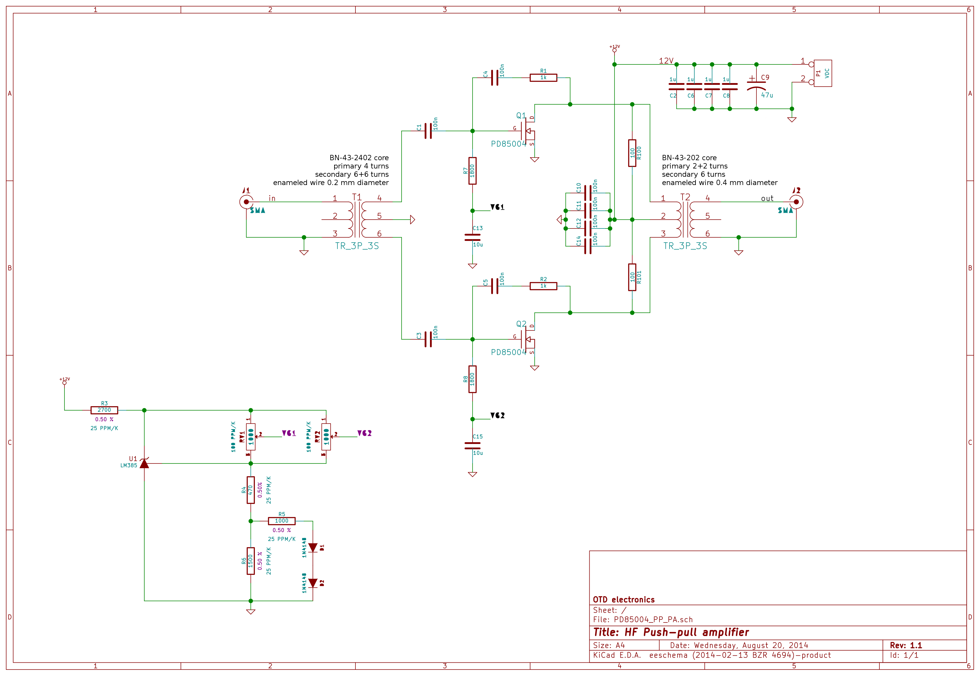
Note that, compared to the basic schematic of the previous version two resistors, R100 and R101, were added to tame some instability that showed up at high power levels. This issue was not seen on the previous version, probably due to the different components used (I suspect the old leaded capacitors were more lossy and this reduced the high-frequency gain enough).
The instability manifested itself either as an auto oscillation above 150 MHz when setting the drain current with the other LDMOS turned off or as a lot of spurious around the main tone(s) at high power level during normal use.
The relatively complex bias circuitry in the lower-left corner is used to generate the gate bias with the right temperature dependency needed to keep the LDMOS current (almost) constant over temperature. On my prototypes I have measured a gate voltage temperature coefficient of -2.65 mV/°C (at 100 mA of drain current), which equates to about 680 ppm/°C; since this figure is of the same order of magnitude of the temperature coefficient of standard resistors and voltage regulators, I used precision parts which have a reduced temperature sensitivity.
The bias point stability is quite good, the drain currents remain within ±5 mA of 100 mA for a wide range of ambient temperatures; when the amplifier is used at high power levels for extended periods of time the drift is larger, due to the thermal resistance between the LDMOS junctions and the temperature sensing diodes.
The PCB top layer, as seen in the KiCad PCB application is shown in the following picture:
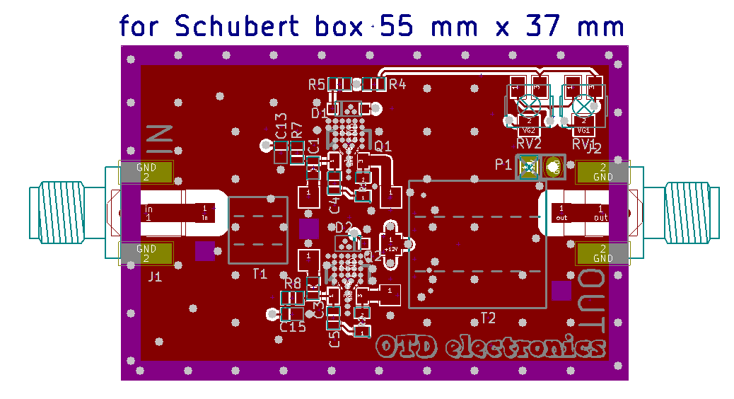
The PCB thickness chosen is 1.0 mm, since this should reduce somewhat the thermal resistance between the LDMOS thermal pad and the enclosure (due to the shorter vias to the ground plane below); probably also a thickness of 0.8 mm is suitable.
Here is how the finished amplifier looks like:

inside the box, the PCB top layer:

A closer look of the PCB top layer:

the picture above is missing the two 100 ohm resistors used to stabilize the amplifier, which were later soldered directly across the output transformer terminals.
The PCB bottom layer:

since I wanted to avoid to cut the ground plane too much with other traces, which would have increased the thermal resistance from the LDMOS to the enclosure, I used a few jumpers to interconnect some non-critical nets.
I do not have a means of measuring or estimating the thermal resistance between the LDMOS ground tab and the metal case, but judging from the temperature the metal case reaches in a short time after power on, it should be quite low. Actually the case gets quite hot quickly, and it might be better to add a small heat sink to reduce its temperature.
Notes for builders
I soldered the whole top layer with solder paste and a hot plate, while the bottom layer was done by the usual hand soldering, with the PCB on the hot plate at around 100 C to ease the ground connections soldering. It might be possible to solder the PD85004 by heating from the bottom side with a (big enough) soldering iron, but I did not try this.
Actually this amplifier was the first PCB I soldered with on a hot plate; I can now say that it was much easier than I thought. My only suggestion is to check the hot plate temperature settings (mine is very old with an imprecise mechanical control) by doing some test with another PCB; you can use some scrap SMD PCB to check at which actual setting the solder melts.
The resistors R100 and R101 are not mounted on the PCB, normal leaded resistors should be used for them (1/4 W or larger recommended).
Note that, up to revision 1.1, the silkscreen on the PCB for the two diodes D1 and D2 was wrong, the white band was on the anode side instead of the cathode.
Setting the bias current is tricky; due to the big temperature sensitivity of the devices and to the thermal feedback thru the diodes and the other components, the drain currents of the two devices cannot be set separately. The easiest way is with two amperometers, one in series with the drain of each device. The output transformer needs of course to be disconnected from the drains, while the two 100 ohm resistors in parallel with the drains should remain in place, as they are needed to stabilize the amplifier when adjusting the bias (when one device is off the other is less loaded so this latter is more prone to oscillations).
The amplifier runs quite hot and a metallic enclosure in good contact with the PCB ground is recommended to provide a good heat sink. In the tin box I have used the PCB ground plane periphery is soldered to the enclosure all around. In case you do not plan to use the same Schubert tin box I have used (I don't think those are popular ouside of Europe) the PCB size could be adjusted to fit a similar enclosure.
Amplifier PCBs manufacturing files
In case you prefer to order directly from a PC prototyping service, here is a zip file containing all the needed Gerber and drill files originally used for ordering the PCBs show above.
Later I have also corrected the bottom-side SMA solder mask and other minor stuff (silkscreen) in a more recent version which I did not send to fabrication, since I have already enough PCBs; there shouldn't be any errors anymore in this latest version, but please check carefully before using it anyway...
Amplifier PCBs for sale
Since the minimum order quantity from Elecrow is 10 pieces, I have now several PCBs left that I do not plan to use:
PCBs are sold out!

These are the 1.0 version PCBs, the only one that I had fabricated, which might need a simple rework to remove the solder mask on the bottom side for the SMA legs, if you would like to solder them also there.
If you would like to have one, just send me a mail, I will ship you one PCB at cost (about 1.5 euro plus shipping).