IN3OTD's web site
...under perpetual construction.

Wideband push-pull low-power amplifier measurements
Under construction...
After playing with the class-A amplifier using a PD85004 as active element, I have built a push-pull (class-AB) version; actually, several variations of the base schematic.
All the amplifier variants use a 12 V supply, 100 mA quiescent drain current (per-device) and the same input and output transformers, built as follows:
- input transformer : BN-43-2402 core; primary 4 turns, secondary 6+6 turns; enameled wire 0.2 mm diameter (do not use a thicker wire, the core holes are almost completely filled by the windings)
- output transformer : BN-43-202 core; primary 2+2 turns, secondary 6 turns; enameled wire 0.4 mm diameter
The measurements results for all the amplifier versions are shown below: here are the links to the data for each version:
- with center-tapped input transformer and gate swamping resistors
- input transformer without center tap and gate swamping resistors
- with center-tapped input transformer and gate-drain feedback
- input transformer without center tap and gate-drain feedback
As shown in the following, these slightly different versions can have very different intermodulation performances.
The PD85004 is a nice device, with a high bandwidth and gain, but has its Achilles' heel in the thermal management: its stated junction-to-case thermal resistance is 21°C/W, which might not seems much, but coupled with the high drain current temperature sensitivity can cause the bias point to drift a lot. Just to make an example, the gate-source temperature coefficient (measured, at 100 mA drain current) is around -2.65 mA/°C, while the device transconductance is about 0.3 A/V; this means that, when the device is soldered to an ideal heat sink with no thermal resistance to ambient, the drain current will change about 0.8 mA/°C, quite a good thermometer. In practice the current change will be even greater, due to the finite thermal resistance between the device case and the ambient.
But, worse of all, this means that when one of the amplifiers described here is providing the full output power, and each device will be dissipating around 2.5 W, the internal junction temperature will rise more than 50°C above ambient and the drain current will tend to increase several tens of milliamperes above the quiescent value!.
Center-tapped input transformer with gate swamping resistors
The very simple schematic is shown below:

there is really not much more to it, even if it will be better to add some component to improve the high-frequency stability, as some gate series resistor or additional resistive loading on the drains, even if this particular version did not show signs of instability. The circuit was built on a bare PCB:

Intermodulation products at 1 W PEP output:

Intermodulation products at 4 W PEP output:

Measured small-signal S-parameters (with -20 dBm input):
 .
.
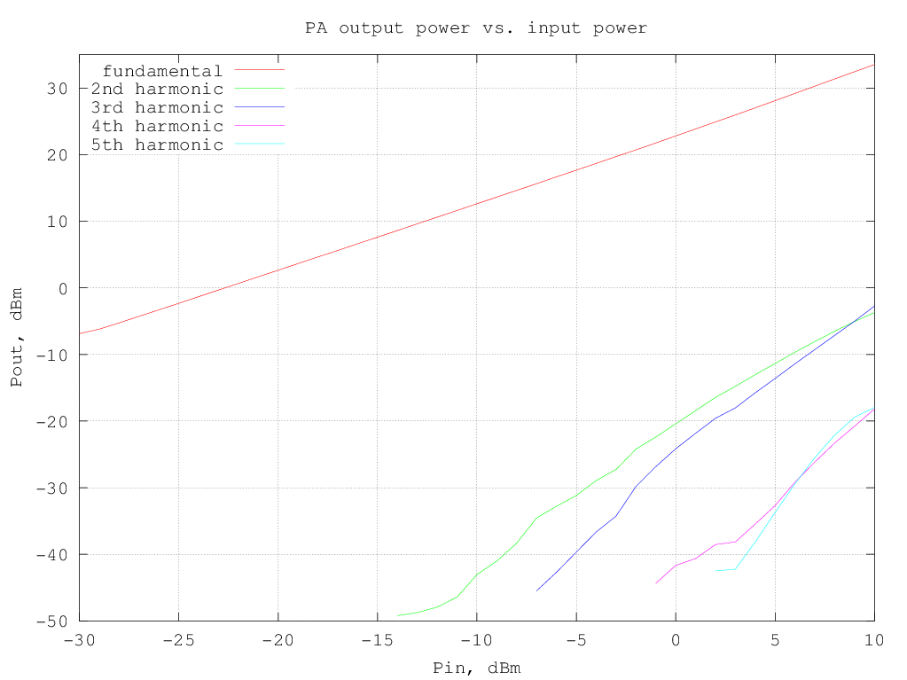
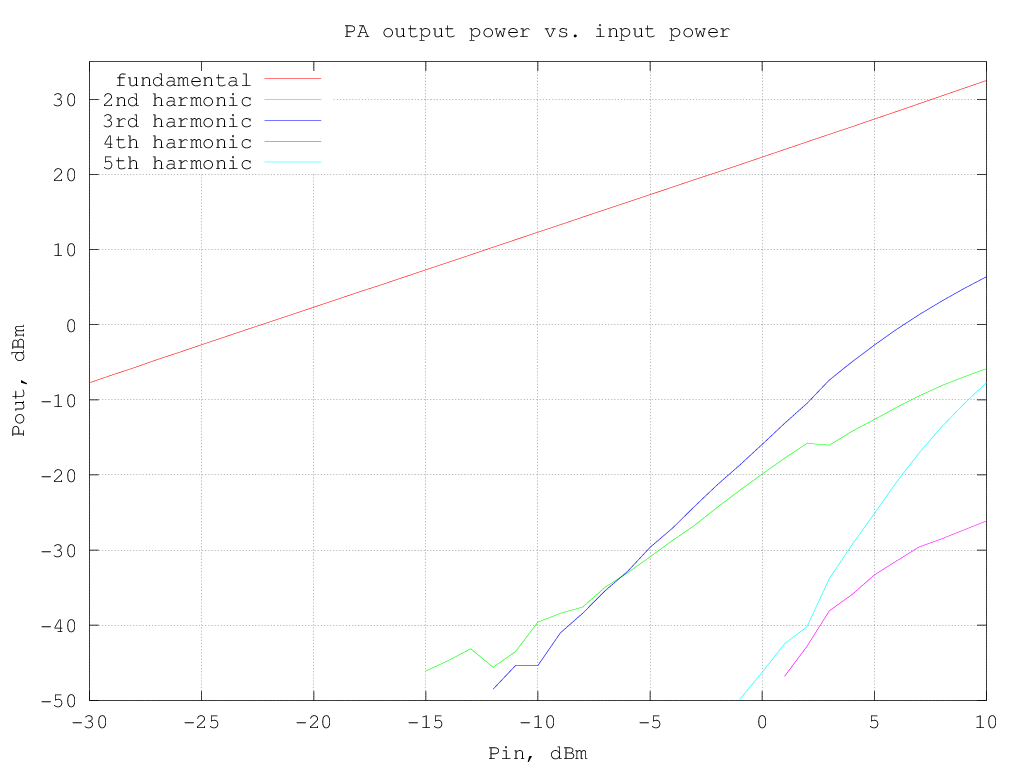
The fundamental and harmonics output levels versus input power, with a 10 MHz sinewave input, is shown in the graph below:
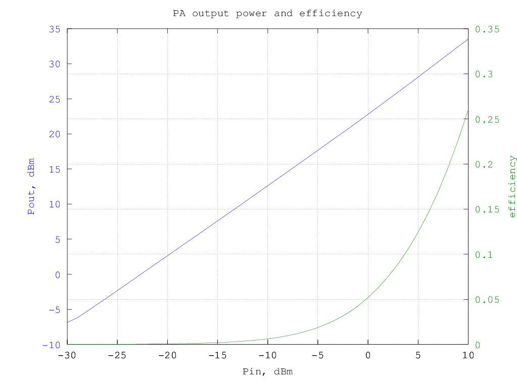
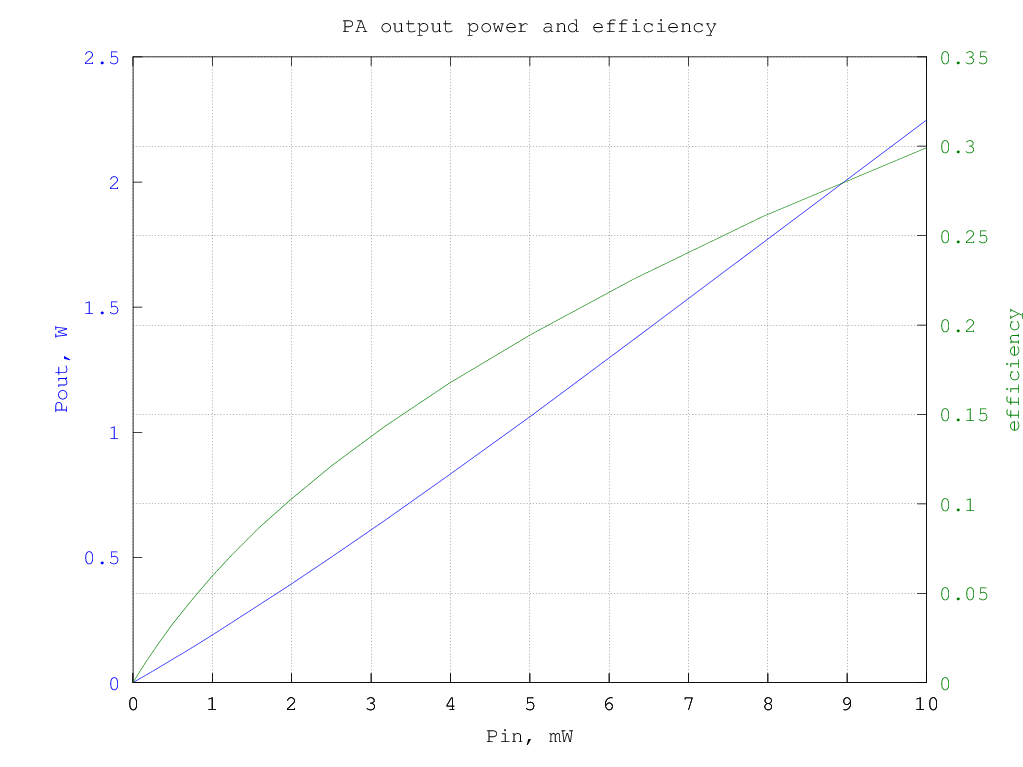
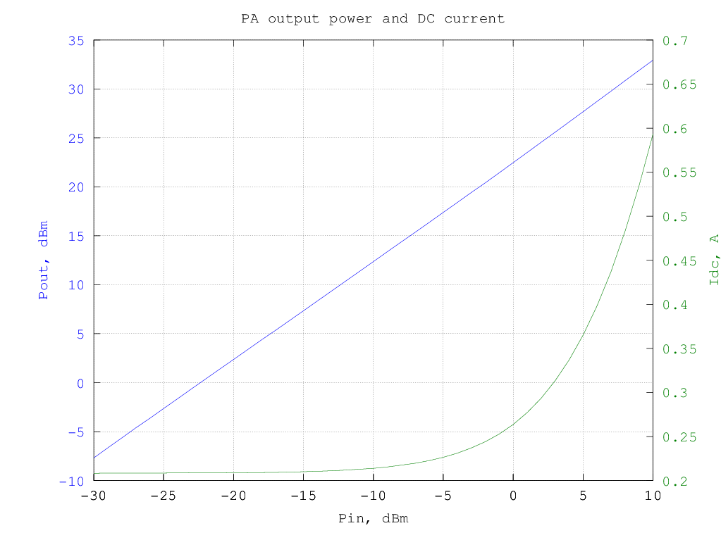
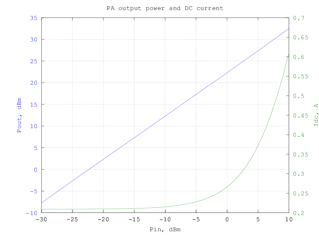
RF output and DC current drawn from the supply versus input power (10 MHz sinewave) are shown in the following graph:

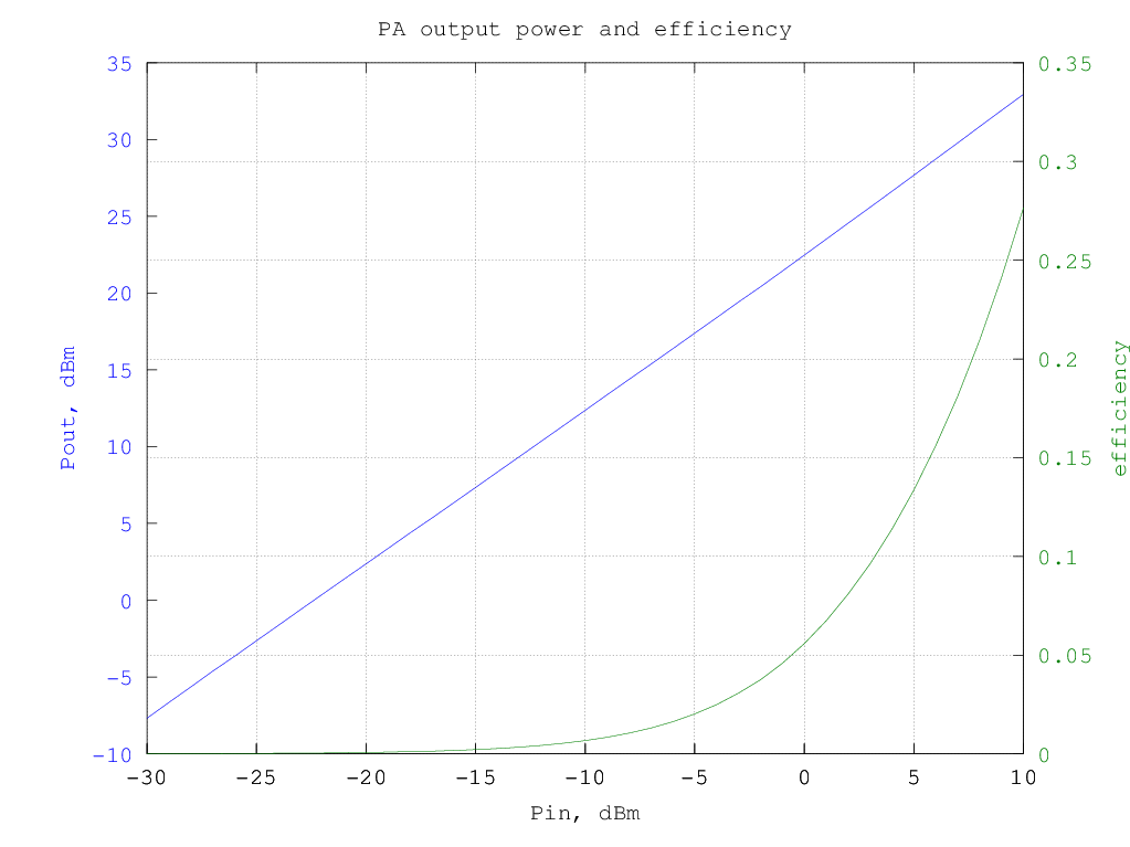
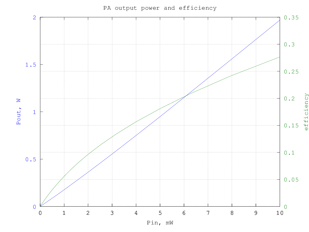
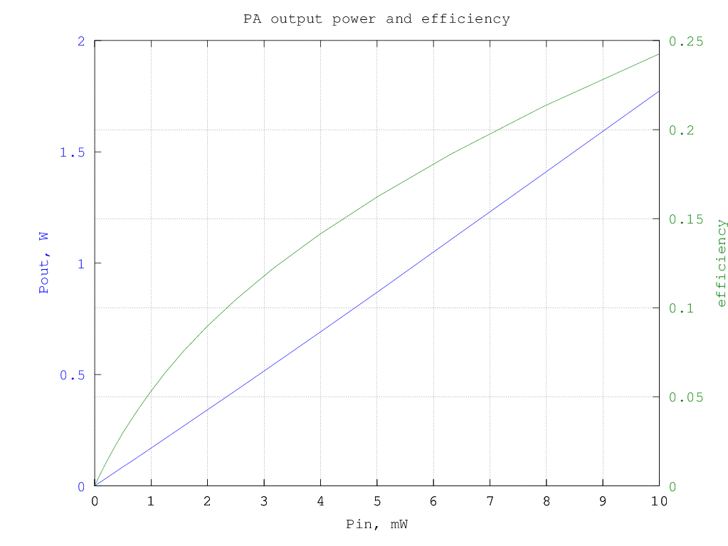
and the resulting efficiency is shown in the graphs below (data are the same for the two graphs, in the first the input and output power are in dBm and in the second they are in watt):
The third-order intermodulation products amplitude w.r.t the output power are shown in the graph below (note that the output power is per-tone, so to have the actual [average] power multiply the value by two, to have the PEP, multiply by 4):


Input transformer without center tap and gate swamping resistor
Schematic is the same as the previous variant, only the input transformer center tap has been left unconnected.
Unfortunately I do not have much data on this version, since it proved to be somewhat unstable. With a small signal at the input (< 0 dBm) it appeared to work normally, but as soon as a higher level was applied it started oscillating at around 150 MHz and didn't stop even when the input signal was removed. As said at the beginning, I should probably have added some additional components to reduce the gain at high-frequency, but did not have much time to experiment...
With center-tapped drive transformer and resistive feedback
In this variation of the amplifier the input impedance is set by using a resistive feedback on the active devices, instead of using the low-value resistors on the gates:

The idea was that using feedback to establish a resistive input impedance instead of wasting power on the gate swamping resistor should help in improving the amplifier linearity. Or not ? (see below)
Intermodulation products at 1 W PEP output:

Intermodulation products at 4 W PEP output:

Measured small-signal S-parameters (with -20 dBm input):
 .
.
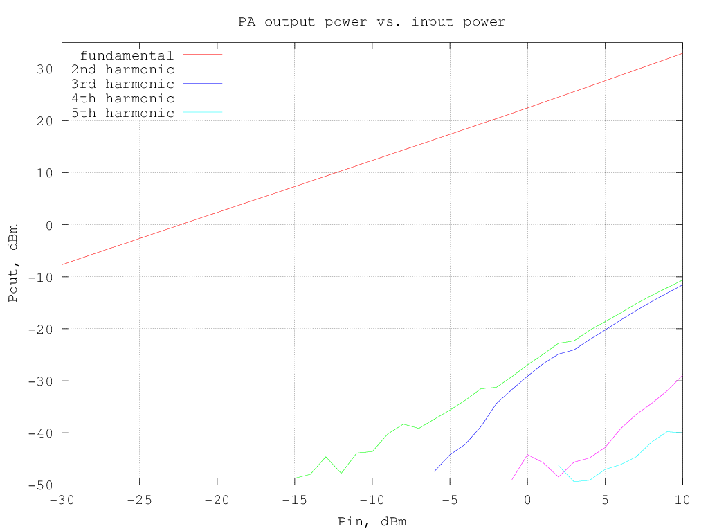
The fundamental and harmonics output levels versus input power, with a 10 MHz sinewave input, is shown in the graph below:
RF output and DC current drawn from the supply versus input power (10 MHz sinewave) are shown in the following graph:
and the resulting efficiency is shown in the graphs below (data are the same for the two graphs, in the first the input and output power are in dBm and in the second they are in watt):
The third-order intermodulation products amplitude w.r.t the output power are shown in the graph below (note that the output power is per-tone, so to have the actual [average] power multiply the value by two, to have the PEP, multiply by 4):

The graph below shows the relative amplitude of the IMD products (separately for upper and lower products; note that the 5th-order products are barely visible just above -70 dBc) for a two-tone test with varying tone spacing (the output power is 1 W PEP)
 except for the dip around 250 kHz (likely due to the output transformer center-tap bypassing), the IMD level appear quite constant; there is still some unexplained variation at very low frequencies .
Input transformer without center tap and resistive feedback
Schematic is the same as the previous variant, only the input transformer center tap has been left unconnected.
Intermodulation products at 1 W PEP output:

Intermodulation products at 4 W PEP output:

Measured small-signal S-parameters (with -20 dBm input):
 .
.
The fundamental and harmonics output levels versus input power, with a 10 MHz sinewave input, is shown in the graph below:
RF output and DC current drawn from the supply versus input power (10 MHz sinewave) are shown in the following graph:
and the resulting efficiency is shown in the graphs below (data are the same for the two graphs, in the first the input and output power are in dBm and in the second they are in watt):
bb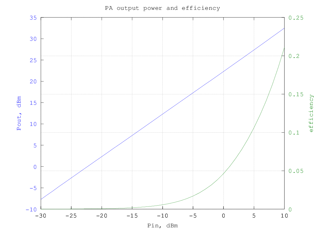
The third-order intermodulation products amplitude w.r.t the output power are shown in the graph below (note that the output power is per-tone, so to have the actual [average] power multiply the value by two, to have the PEP, multiply by 4):

Performance comparison with and without feedback
The graphs below show the intermodulation distortion products for the different circuit configurations.
Surprisingly, the resistive feedback version achieves the lowest distortion only if the input transformer is center tapped, otherwise its performances are much worse. I do not have a solid explanation of this, I think it is probably related to the nonlinear input impedances presented by the devices which are reflected differently on the other device whether the input transformer is center tapped or not. Time for other experiments...


References:
| [1] | Steve C. Cripps, "RF Power Amplifiers for Wireless Communications, 2nd ed., Artech House, 2006 |
| [2] | "Thermal behavior of small-signal discretes on multilayer PCBs," NXP Application note AN11076. |