IN3OTD's web site
...under perpetual construction.

20 W HF PA measurements
Under construction...
HF power amplifier with a push-pull of AFT09MS015N
Quiescent current : 250 mA per device
input transformer : BN43-2402, primary (50 ohm side) 5 t 32 AWG (0.2 mm) : 4t+4t 30 AWG (0.25 mm)
output transformer : BN43-202, primary (MOS side) 1t+1t (0.5 mm) : 5t (0.3 mm)N
Here is a picture of the completed PA:

The PCB has a thickness of only 0.8 mm in order to reduce the thermal resistance between the MOS case, soldered on the top layer ground plane, and the unetched bottom layer.
Some thermal grease was applied on the board bottom side before securing it to an heatsink.
Uncompensated PA performance
PA characteristics without HF compensation on the output transformer.
The (small-signal) gain of the amplifier is around 26 dB in the lower HF band and goes down to about 24 dB on the higher end and still around 21 dB at 50 MHz. Its input matching is relatively good at the lower HF and degrades above 10 MHz.
The data above are summarized in the following picture; all data were measured with -30 dBm at the PA input (i.e. approximately -4 dBm output):
 .
.
note the very good agreement between measurements and simulation; the simulation was using the measured coupling transformers data and a small-signal model for the FETs.
For the high-power measurements the output of the amplifier was terminated in a suitable wideband dummy load, so that its output was loaded by a 50 ohm resistance at all frequencies of interest; actual performances when using a low-pass/bandpass filter at the output (which should normally be used if you plan to use the PA "on air") might be slightly different, as the harmonics will not see a pure 50 ohm resistance and the active devices current and voltage waveforms could be somewhat different.
1.8 MHz measurements
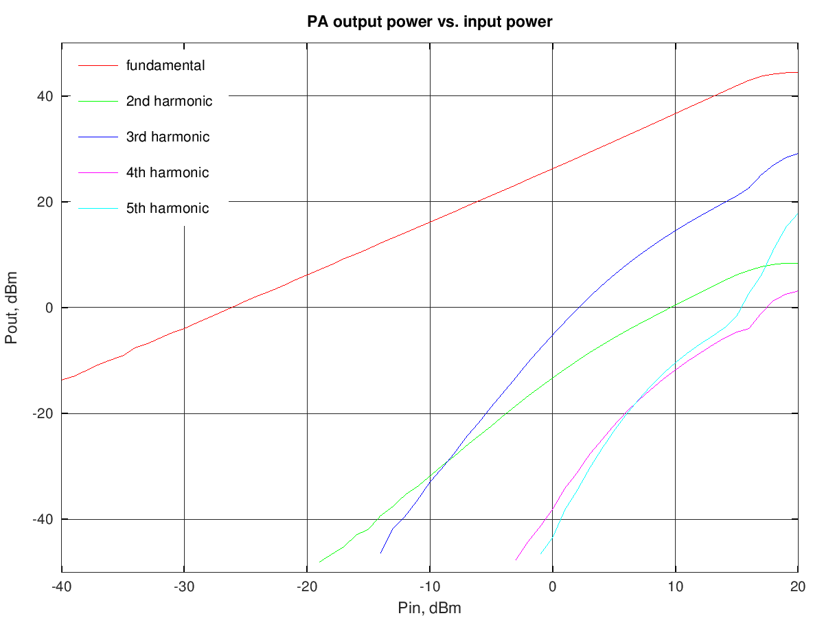
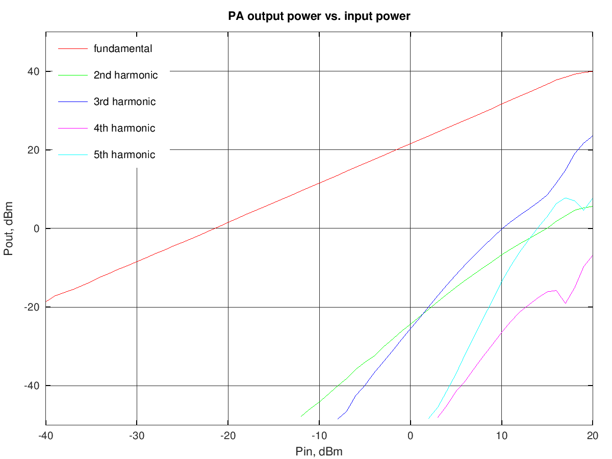
The fundamental and harmonics output levels versus input power, with a 1.8 MHz sinewave input, is shown in the graph below:

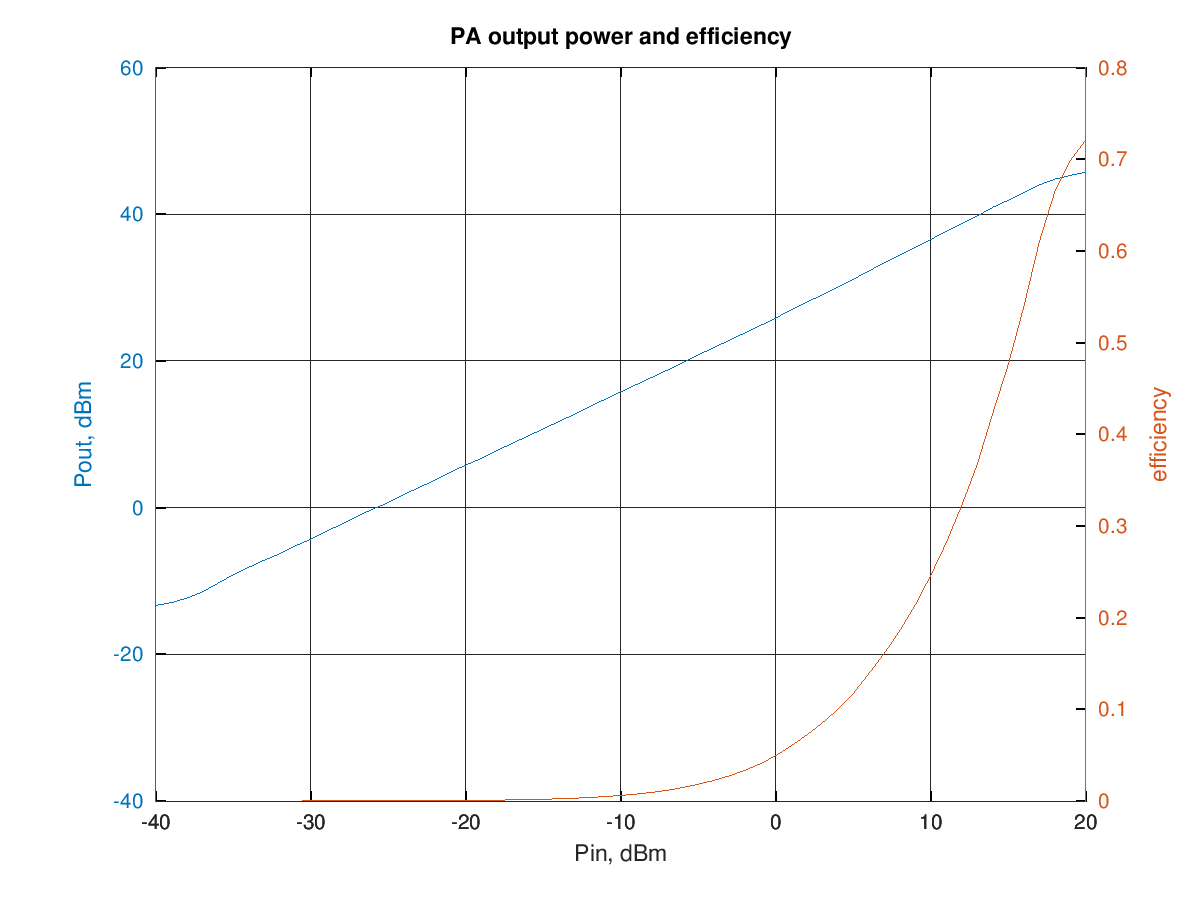
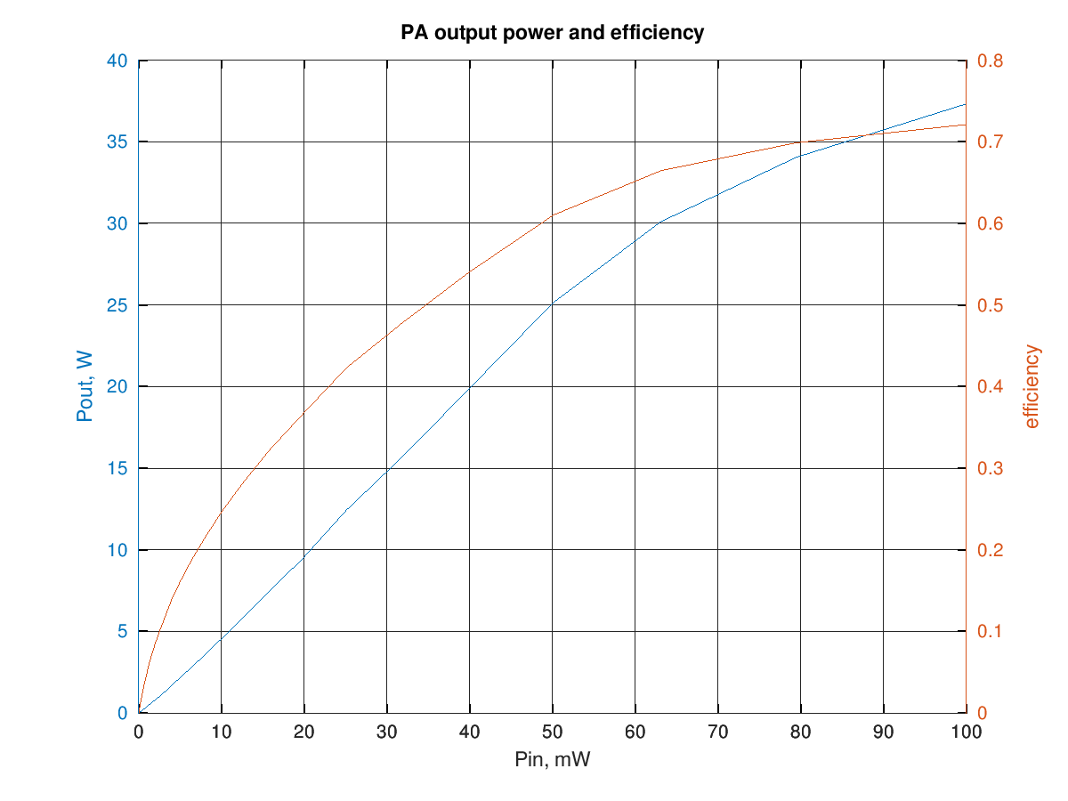
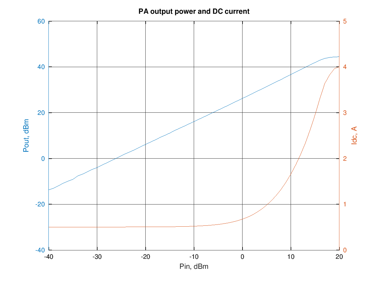
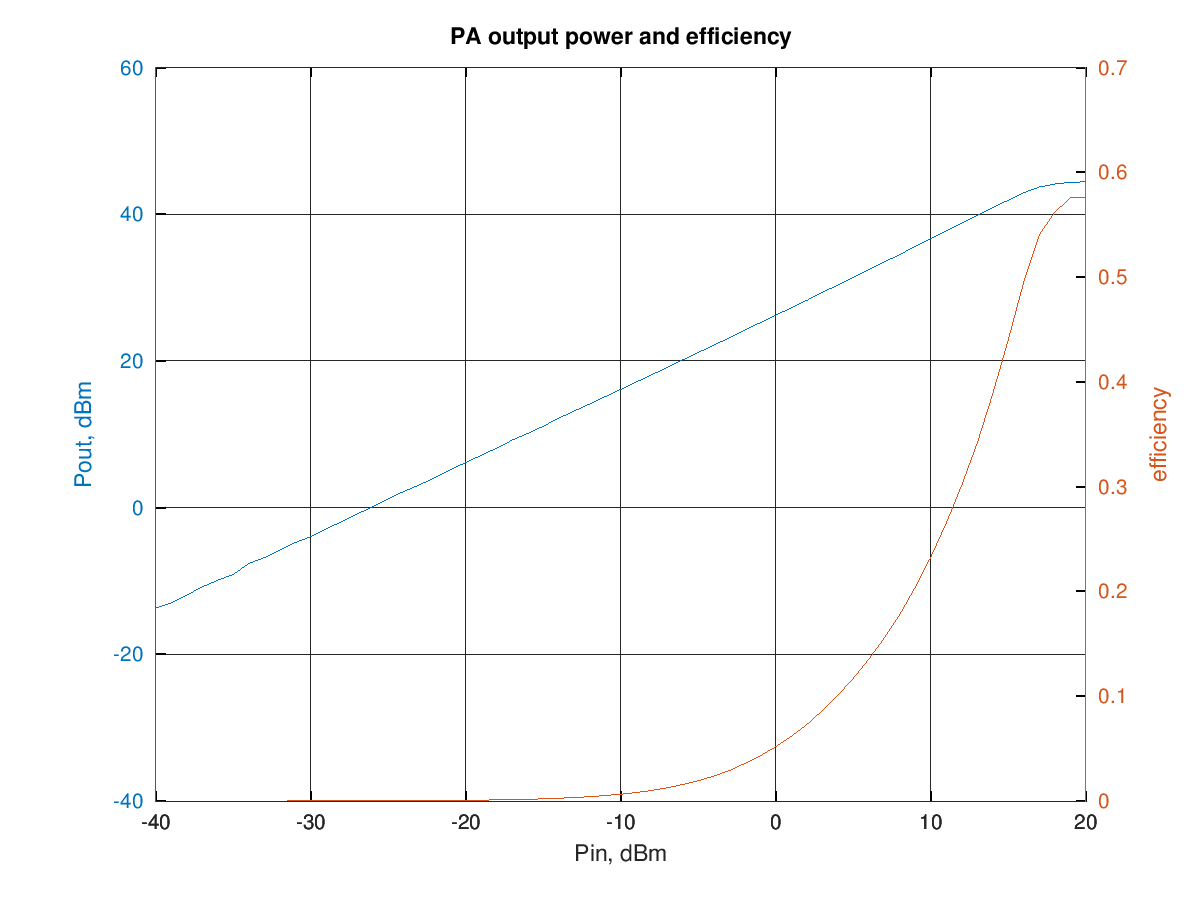
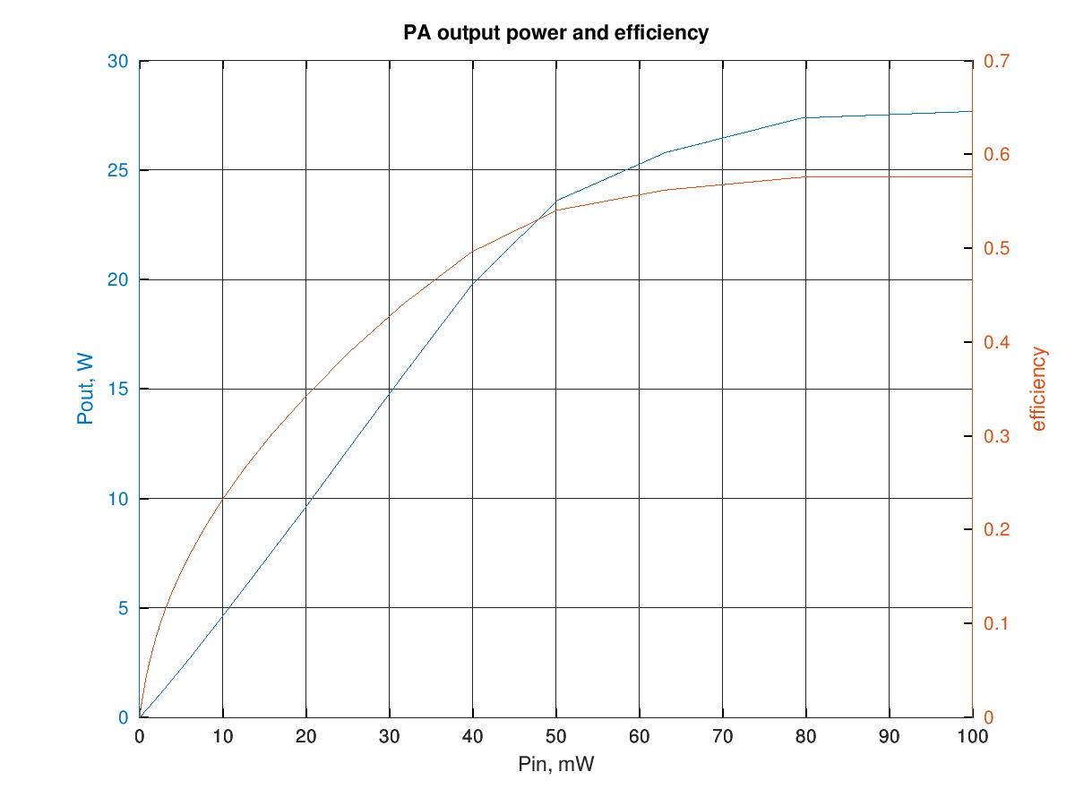
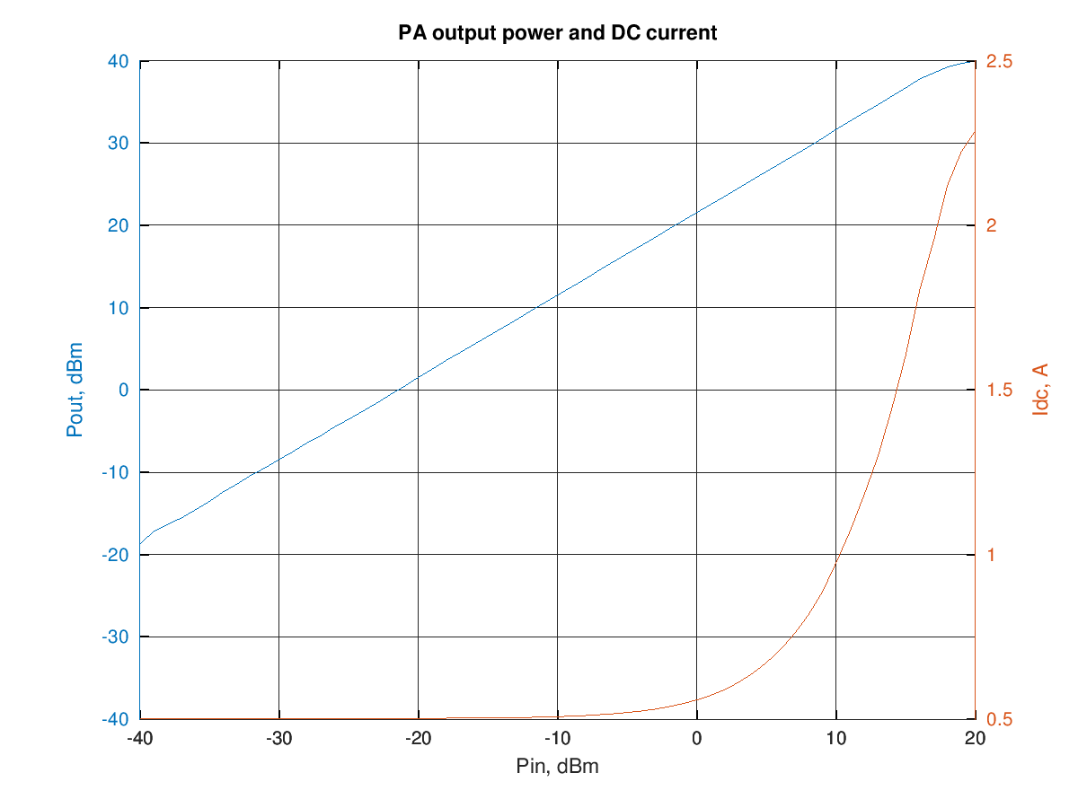
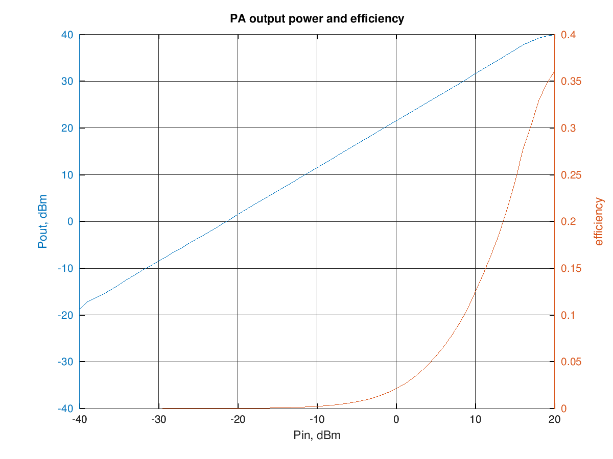
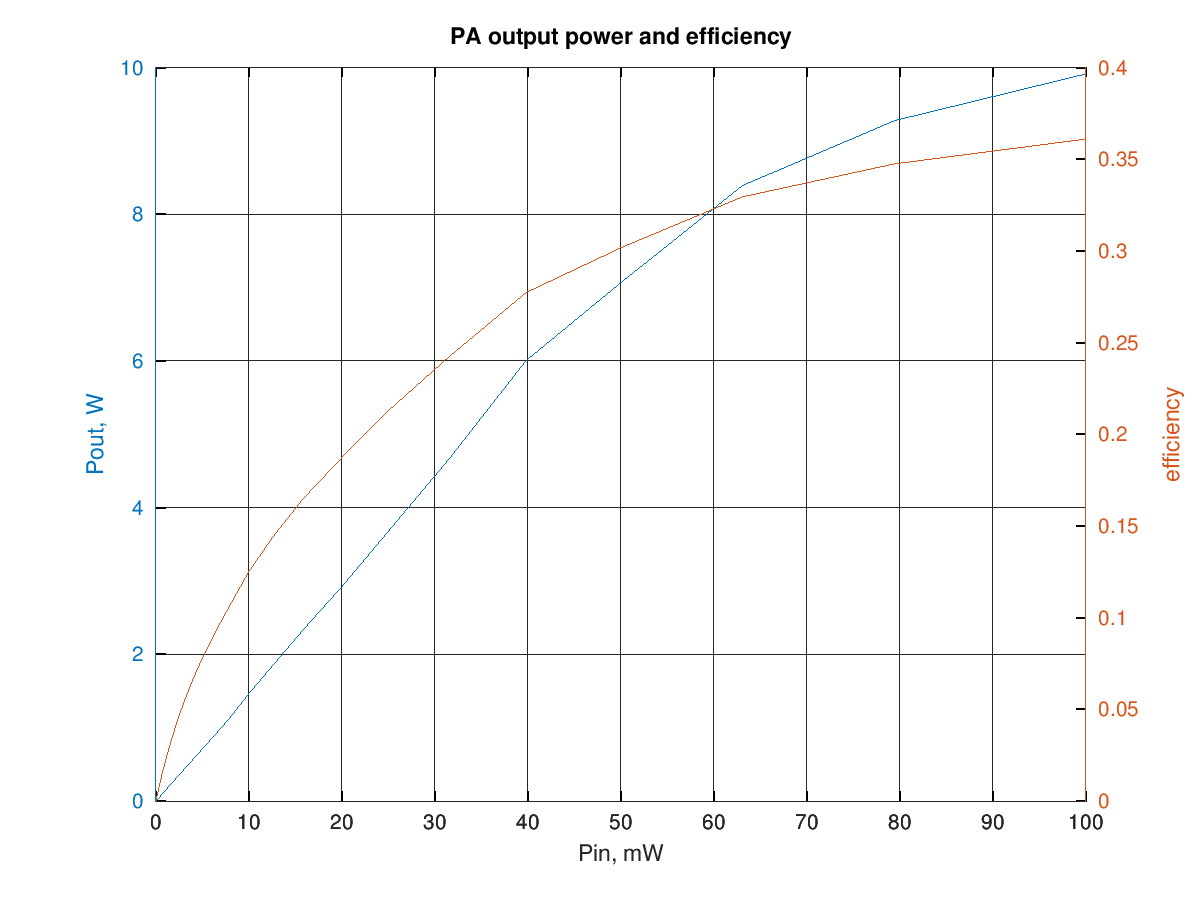
RF output and DC current drawn from the supply versus input power (1.8 MHz sinewave) are shown in the following graph:

and the resulting efficiency is shown in the graphs below (data are the same for the two graphs, in the first the input and output power are in dBm and in the second they are in watt):
The graph below shows the relative amplitude of the IMD products (separately for upper and lower products) for a two-tone test with varying tone spacing at 3.7 W PEP output:
 the upper and lower IMD tones amplitude are significantly different at large spacing and have a large variation with frequency; this is likely due to interactions between the bias network baseband impedance and thermal effects.
10 MHz measurements
The fundamental and harmonics output levels versus input power, with a 10 MHz sinewave input, is shown in the graph below:
RF output and DC current drawn from the supply versus input power (10 MHz sinewave) are shown in the following graph:
and the resulting efficiency is shown in the graphs below (data are the same for the two graphs, in the first the input and output power are in dBm and in the second they are in watt):
The graph below shows the relative amplitude of the IMD products (separately for upper and lower products) for a two-tone test with varying tone spacing at 7.1 W PEP output:
 the upper and lower IMD tones amplitude are significantly different at large spacing and have a large variation with frequency; this is likely due to interactions between the bias network baseband impedance and thermal effects.
30 MHz measurements
The fundamental and harmonics output levels versus input power, with a 30 MHz sinewave input, is shown in the graph below:
RF output and DC current drawn from the supply versus input power (30 MHz sinewave) are shown in the following graph:
and the resulting efficiency is shown in the graphs below (data are the same for the two graphs, in the first the input and output power are in dBm and in the second they are in watt):
The graph below shows the relative amplitude of the IMD products (separately for upper and lower products) for a two-tone test with varying tone spacing at 3.0 W PEP output:
 the upper and lower IMD tones amplitude are significantly different at large spacing and have a large variation with frequency; this is likely due to interactions between the bias network baseband impedance and thermal effects.
Effect of transformer compensation
The PA response at the higher end of the HF is down a few decibels, due to device input capacitance and mainly to the output transformer.
Tipically the output transformer response is compensated by adding a capacitance in parallel with the low-impedance winding. Here below are several graphs showing the effect of various values of the transformer compensation capacitance on the PA performance at 30 MHz.
The PA gain at 30 MHz initially increase with increasing values of the compensation capacitance but starts to decrease after reaching a good flatness with a capacitance of about 400 pF:

The compensation capacitance affects also the PA third-order intermodulation. With no or little compensation capacitance the two-tone IMD is very high and the maximum output power limited: increasing the capacitance the IMD decreases and the maximum output power increases but the two parameters do not reach their optimum for the same value of capacitance. A good compromise between maximum output power and minimum IMD is reached for a capacitance of about 450 pF:

the output power in the graph above is per-tone.
Also the efficiency, measured with a single tone at the input, is affected by the compensation capacitance: again a good compromise is reached for values between 400 pF and 450 pF:

Temperature measurements
Here are some measurements of the output transformer and MOS devices for the compensated PA (Cc = 400 pF) at several frequencies.
Thermocouples were placed on the output transformer ferrite and on one of the MOS devices plastic body, as shown in the following picture:

The power amplifier was left on with only the device bias current and no input signal to stabilize the temperature and then an input signal applied as to obtain about 10 W at the output was applied for about 30 minutes. Then the input signal was removed and the amplifier left to cool down for about 20 minutes. The temperature read by the two thermocouples, the output power and the overall current consumption were recorded during the entire experiment duration.
The graph below shows the evolution of the output transformer and MOS device temperature for different frequencies of the input signal.

Note that at 1.8 MHz and 10 MHz the behaviour is quite similar, while at 30 MHz the MOS temperature is significantly lower and the output transformer temperature slightly higher.
The PA efficiency at 30 MHz is also higher, at this output power level.
Output transformers
- BN43-202: AL=2200 nH/turn2
- BN43-3312: AL=7000 nH/turn2
- BN43-7051: AL=10000 nH/turn2