IN3OTD's web site
...under perpetual construction.

Hermes-Lite SDR - frontend v1.4 measurements
Under construction - design is not yet final...
Measurements on the frontend v1.4 designed by James Ahlstrom, which is an evolution of the frontend v1.3 using a dual opamp for higher output power. Details on the design are in this discussion thread.
This is the frontend v1.4 schematic, from N2ADR, used as a reference for the circuit characterized on this page:

only the TX portion has been built, with its output connected directly to the output SMA connector. The on-board regulator was not used and the +10 V supply came from an external regulated power supply.
Note: since the PCB for the frontend v1.4 is not yet available, the circuit was build using the 1.3 PCB with a small added part with the dual opamp, built "dead-bug style".
This may have an impact on the actual performances and the final implementation on the v1.4 PCB should be measured to verify if there are any major deviations.
This is how the actual circuit looked like:

Hermes-Lite with Frontend v1.4 output
The following graphs show the frontend TX output measured when driven by the Hermes-Lite v1.22 board. The firmware FPGA FW version used was the 20160220_txdac/CVA9/, half-duplex. The system clock frequency fs was 73.728 MHz
Output vs. TX frequency


See below for the measurements with an improved filter.
Output vs. TX drive level
Changing the TX drive level, which changes the TxDAC gain, see the AD9866 datasheet for details.
TX frequency at 24.895 MHz
Output power at fundamental:

when changing the TxDAC output power (by changing the TxPGA code) the spurs remains adequately suppressed:

Output harmonics and spurs vs. frequency
Graphs showing how some of the TX output spurs and images amplitude changes when the fundamental output amplitude is changed.
TX frequency at 24.985 MHz
The harmonics shown below are generated by the frontend: the ones from the AD9866 TxDAC are filtered out by the frontend filter (above 30 MHz).

The sampling images and spurs are also mostly filtered out by the on-board filter, except of course when they fall in the filter passband. There is also some feedthrough in the filter stopband, probably due to a limited ultimate rejection.


Output vs. TX frequency with improved low-pass filter
The output power drop at higher frequency is caused mainly by the input low-pass filter, which is built using very small inductors (Murata LQW2BASR24J00 and LQW2BASR27J00), having relatively high losses in the HF band (their Q at 30 MHz is around 30).
By removing the 390 Ω termination resistor (R1) and adding some resistor on the filter internal nodes the filter gain can be equalized to obtain a flatter response.
A quick simulation showed that by removing R1, adding 1 kΩ in parallel with C2 and C3 and changing C4 to 100 pF gives a filter with a slightly upward slope, which should be helpful to compensate for the intrinsic TxDAC drop at the higher frequencies.
Here is the measured output power at the fundamental with the modified LPF, compared with the original design:
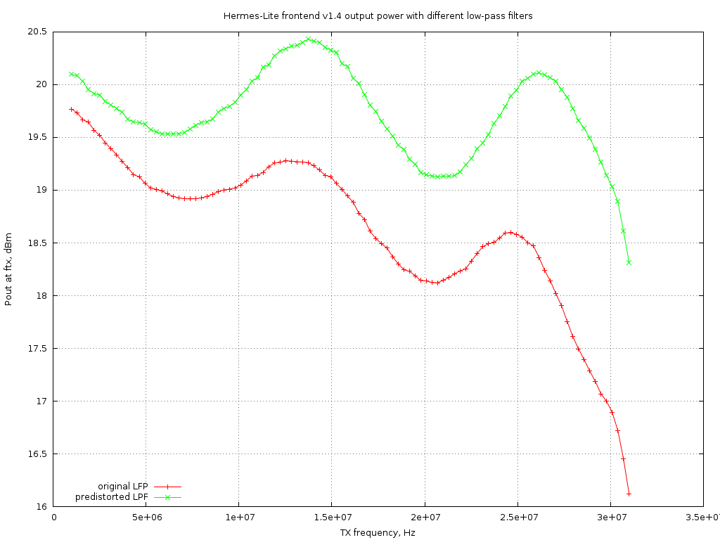
the response is improved but not as flat as expected, likely some other effects should have been taken into account, like the output transformer response or the TxDAC loading. I may try to further optimize the filter, one day...
Standalone tests
The frontend board has also been characterized standalone; input was feed thru a Mini-Circuits ADT1-6T transformer to obtain a differential signal.
Since the frontend is designed to work with the TxDAC output, which is a current source, it does not provide a good match to 50 Ω but this should not change much its distortion.
The frontend was powered using a 10 V regulated supply.
The fundamental and harmonics output levels versus input power, with a 10 MHz sinewave input, are shown in the graph below:
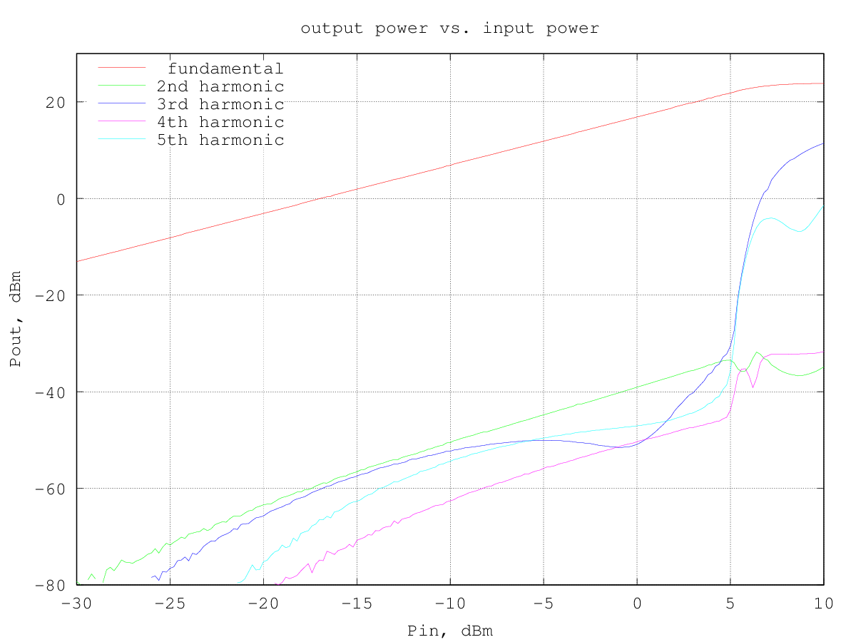
the output power at 1 dB of compression is about 220 mW (23.5 dBm).
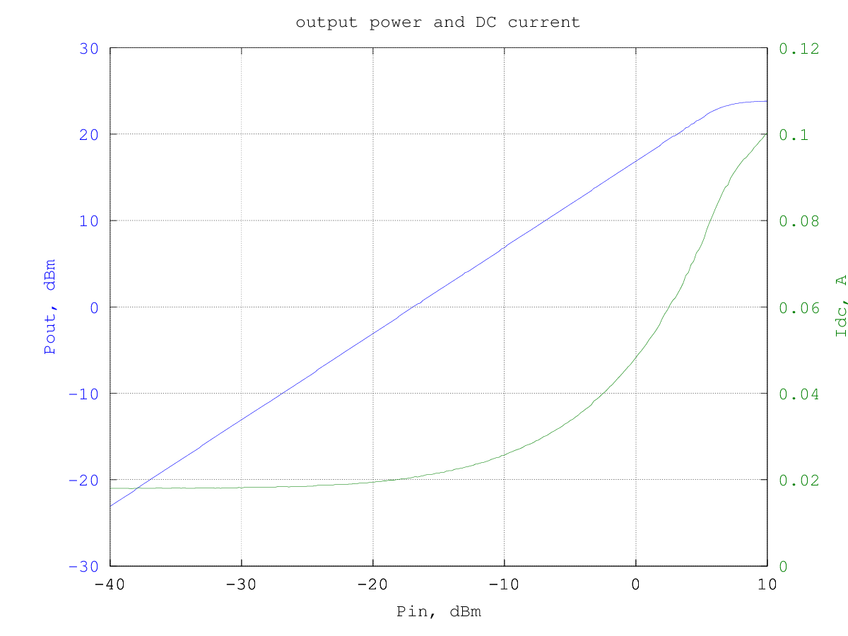
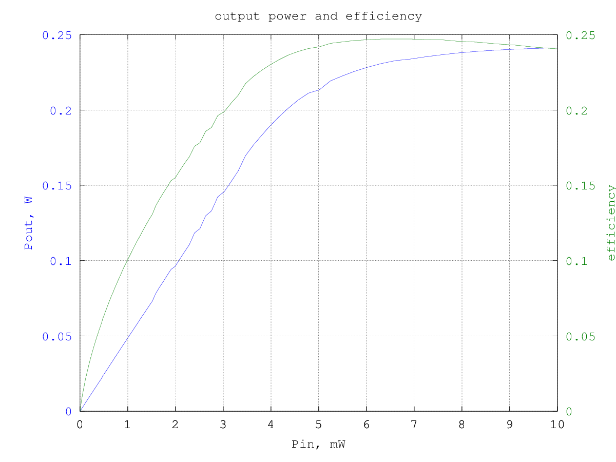
RF output and DC current drawn from the supply versus input power (10 MHz sinewave) are shown in the following graph:
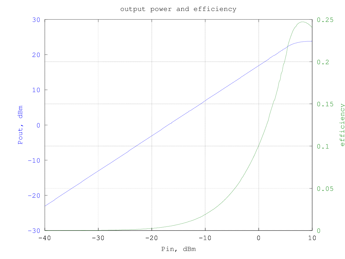
and the resulting efficiency is shown in the graphs below (data are the same for the two graphs, in the first the input and output power are in dBm and in the second they are in watt):
The third-order intermodulation products amplitude w.r.t the output power per-tone is shown in the graph below (to obtain the actual [average] output power multiply the value by two, to have the PEP, multiply by 4):


at an IM3 of -30 dBc the output power is around 60 mW per tone.
The graph below shows the relative amplitude of the IMD products (separately for upper and lower products) for a two-tone test with varying tone spacing at 240 mW PEP output:

IMD level vs. frequency is flat up to about 1 MHz.
By plotting the third-order intermodulation products power vs. the input power we should be able to find the intercept point by extrapolating the results.
Actually for this amplifier the intermodulation products at low input levels are so low that they are completely masked by the noise sidebands of the not-so-clean signal generators used for the test.
Only when the input power is above 0 dBm, the IMD products start to rise out of the noise, with a slope much higher than the usual 3:1. This is typical of amplifiers with a high feedback when driven towards the saturation.

We can only estimate that the IMD products are below a certain level, shown in the graph above, which will give an input IP3 turns of about 33 dBm and a corresponding output IP3 of about 49 dBm.