IN3OTD's web site
...under perpetual construction.

Diode power detectors
I was looking at some forward/reflected power meter circuits, to be used with the Hermes-Lite SDR, and I was wondering how well will a simple diode power detector works at QRPp power levels.
I did a few measurements on a classic circuit, a BAT54 Schottky diode loaded with a 1 MΩ resistor, in parallel with 100 nF. The actual circuit used is shown below:
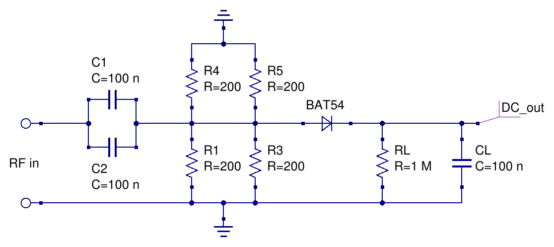
the RF input load resistor was realized with 4 resistors since I wanted to test the detector also with relatively high input power levels, which would have been to much for a single small SMD resistor. I used two coupling capacitors at the input just because the 50 MΩ input line is roughly twice as wide as a single capacitor, but this has no importance at HF, it just looked nicer, hi.
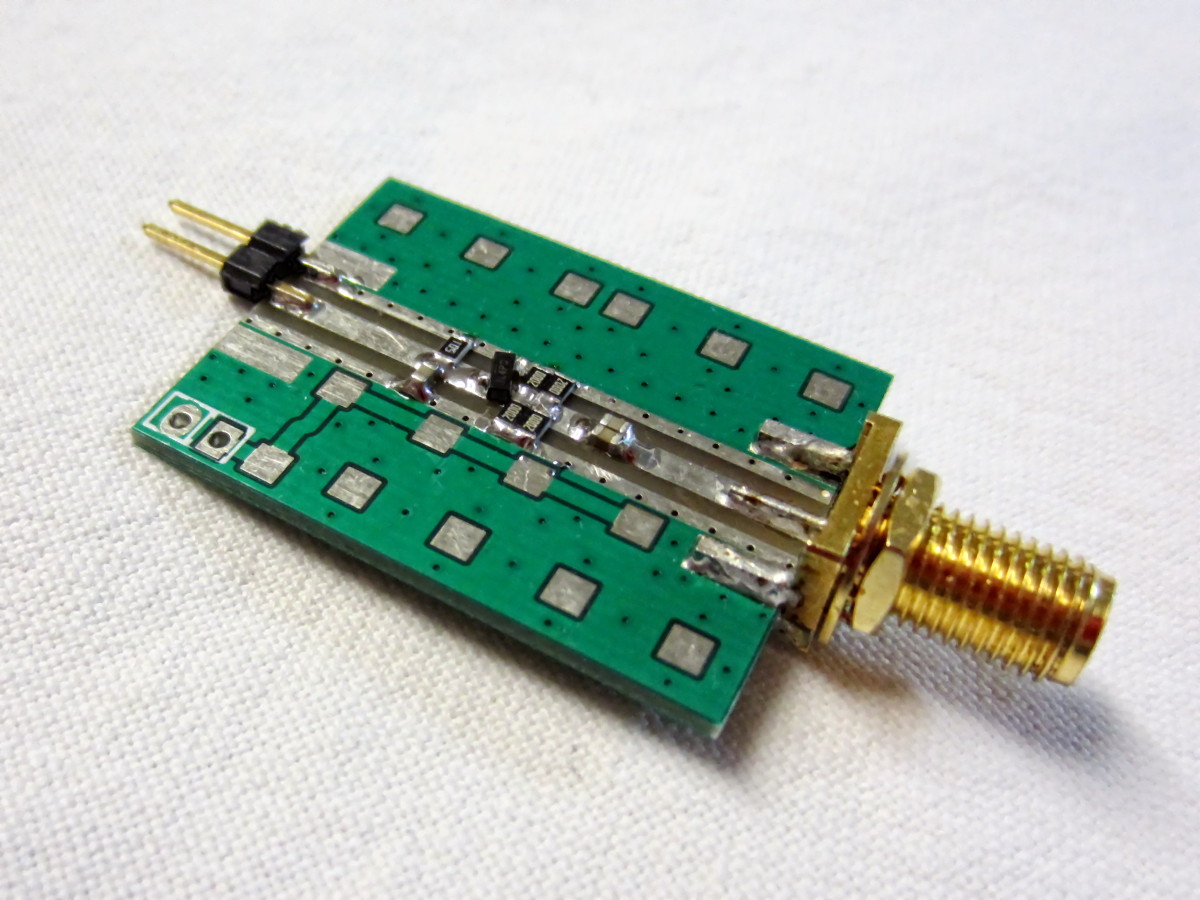
Here are all the components on the test PCB:
At first the power detector was connected directly to the signal generator output and the DC output recorded while sweeping the generator power, for 3 different frequencies - roughly at the beginning, in the middle and at the upper end of the HF band.
As expected, the DC output is quite constant across the HF.
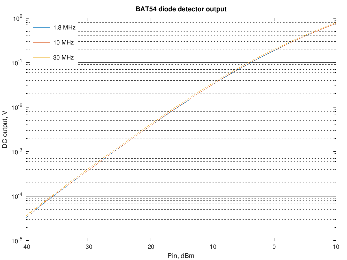
the output was actually slightly higher at 30 MHz, by maybe 0.3 dB, likely due to the signal generator output variation with frequency.
As known, the diode detector output is proportional to the square of the input voltage/linear with the input power at low power levels and becomes proportional to the peak voltage/square root of input power at higher levels. A linear fit of the power detector output voltage to these two regions is shown below:
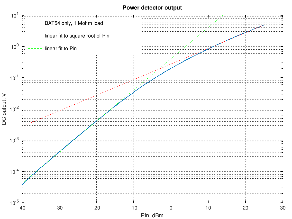
The green dashed line represents an output proportional to the input power, from the function VDC=Pin·kl, where kl was chosen to minimize the fitting error between -40 dBm and -30 dBm.
The red dashed line represents an output proportional to the square root of the input power, from the function VDC=√ Pin ·ks, where ks was chosen to minimize the fitting error between 9 dBm and 19 dBm.
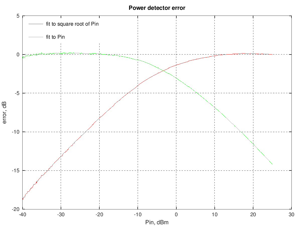
The fitting error for these two lines is shown in the following graph:
Detector response linearization
Ideally the output of the power detector should be proportional to the input power level; as shown above, this is true only at the higher end while at low power levels the output drops significantly.
A quite common circuit used to increase the DC output at low levels uses an op amp with another diode in the feedback path; details of this linearization circuit design are discussed, e.g., in [1].
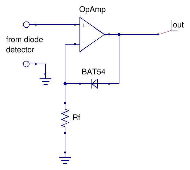
Since at low power levels the diode detector output is very low and its DC output impedance quite high, it's important that the op amp used has a low input offset voltage and a low bias current. The circuit above was built with an old, but still good, TLC27M2C (1.1 mV offset voltage, 0.6 pA bias current - typical).
The typical recommended feedback resistor value is between 1/5 and 1/10 of the diode load resistor value, which is 1 MΩ in this case. Using a 220 kΩ feedback resistor gives this overall output vs Pin:
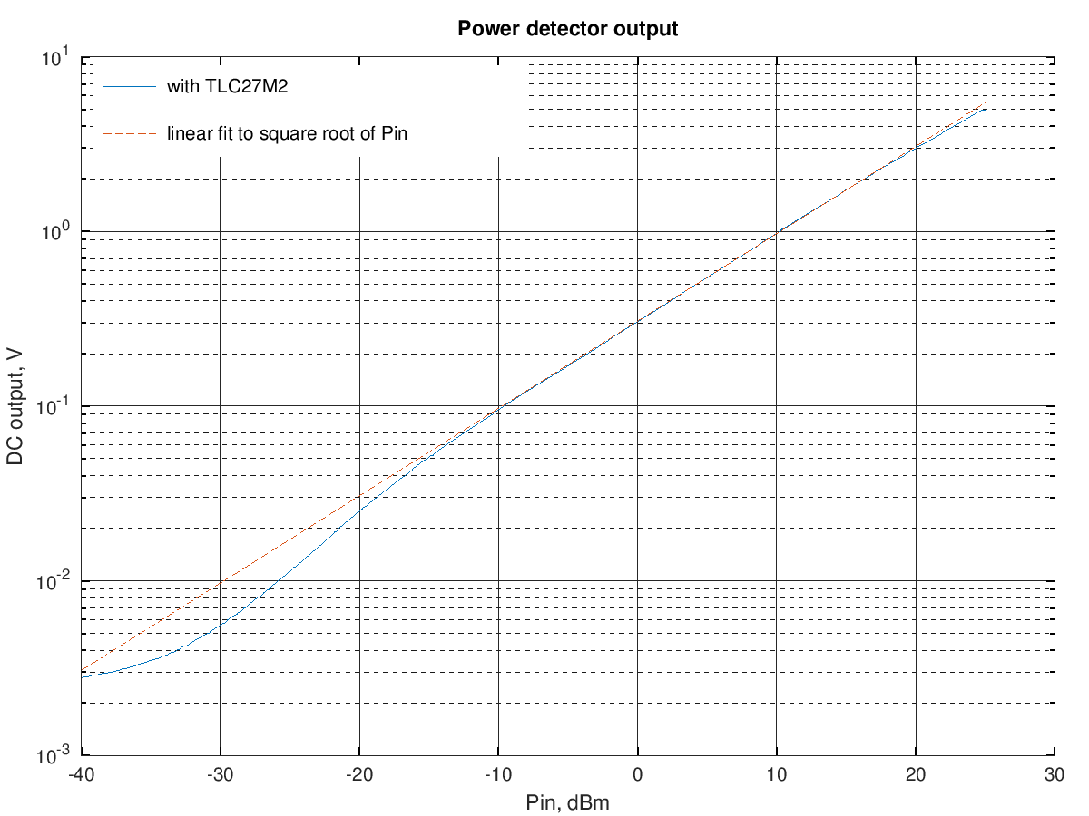
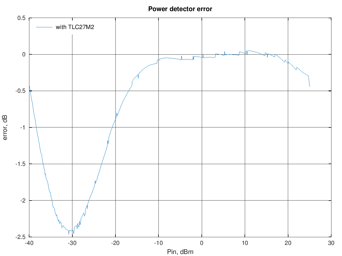
and this is the deviation from the ideal square root of the input power response:
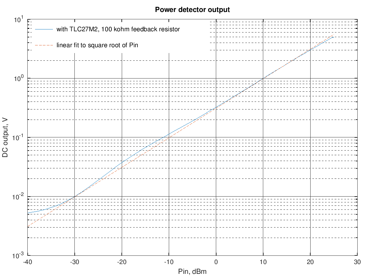
Things looks even better when using a 100 kΩ feedback resistor:
and the corresponding deviation from the ideal square root of the input power response:
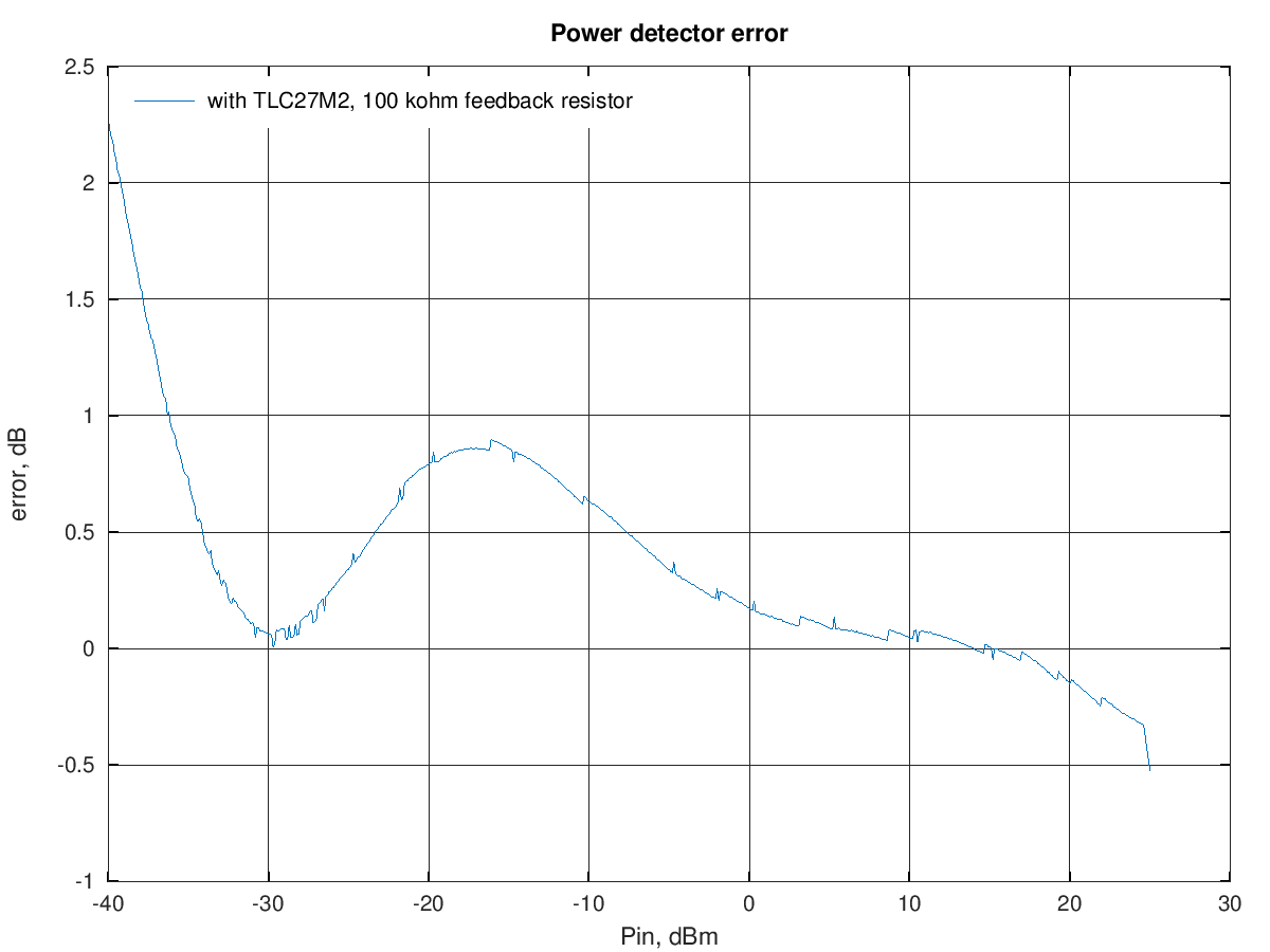
with this feedback resistor value the output follows the RF input voltage linearly with a relatively small error down to around -35 dBm.
Looking at the output error shape between the two feedback resistor values used, it's likely that an even better linearity could be achieved with an intermediate value resistor but I didn't do further experiments with this.
One point that needs to be verified is the temperature dependency of the overall detector output; for sure the bare diode detector output is very temperature sensitive at low power levels: at -40 dBm input I can see the output changing a little when placing a finger near (but not touching) the diode.
Finally, to show the importance of choosing an op amp with a low bias current, here how the overall linearized detector output looks like when using an LMV324 op amp in the linearization circuit (this was the op amp used on the Hermes-Lite v2b3, where all these power detector measurements started from). This op amp has a typical bias current around 15 nA, around 25000 times the TLC27M2 bias current.
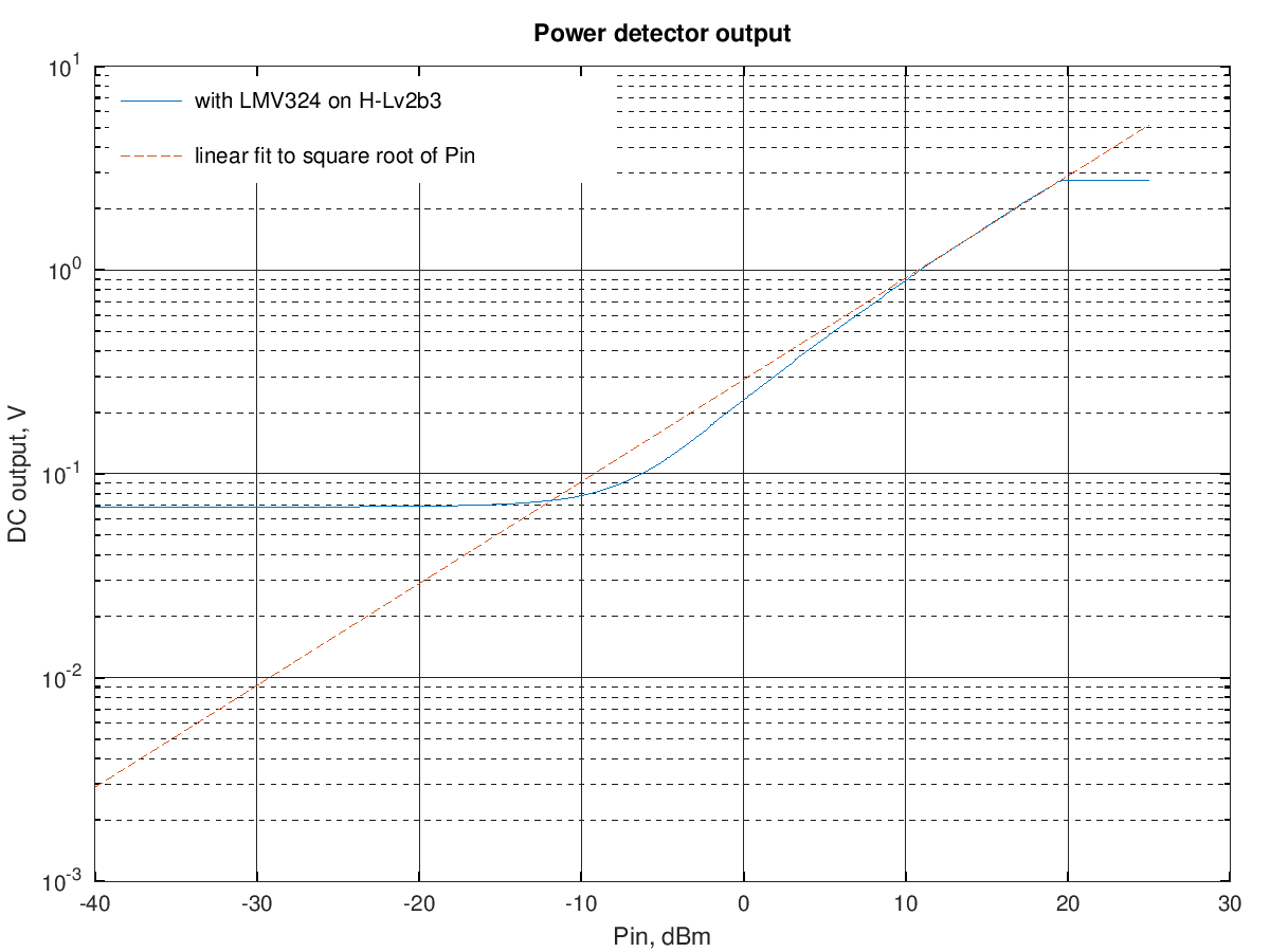
the op amp output has a DC offset of about 50 mV, so below about -15 dBm input the output is independent of the detector input power; this offset likely comes mostly from the op amp input bias current flowing in the 1 MΩ detector load resistor; in fact, a similar offset can be seen at the op amp input when it's connected to the diode detector.
To help choosing a suitable op amp, here is a small table showing the diode detector DC output voltage and the resulting DC current in the 1 MΩ load resistor for a few input power levels:
| Pin, dBm | Vdc | Idc |
|---|---|---|
| -10 | 34.5 mV | 34.5 nA |
| -20 | 4.1 mV | 4.1 nA |
| -30 | 0.42 mV | 0.42 nA |
| -40 | 39 uV | 39 pA |
ideally the op amp input offset voltage and bias current should be much lower than these values to get an accurate reading at the power levels above.
The LMV324 has a low nominal offset (1.7 mV) but a too high bias current (15 nA). Suitable low-cost op amps could be the TSV521(A), TSV911(A) and also the even better but slightly more expensive.AD8691.
A temperature-compensated detector
As noted above, the diode power detector output is quite temperature sensitive, especially at low input power levels. A detector circuit with reduced temperature sensitivity was described in [2] and [3]. Here the basic diode detector is loaded by a network including a diode of the same type so that the DC output temperature dependency cancels out, mostly.
Also for this type of power detector the DC output is proportional to the input power at lower levels and becomes proportional to the square root of input power at high power levels. A linear fit of the voltage to these two regions is shown below:
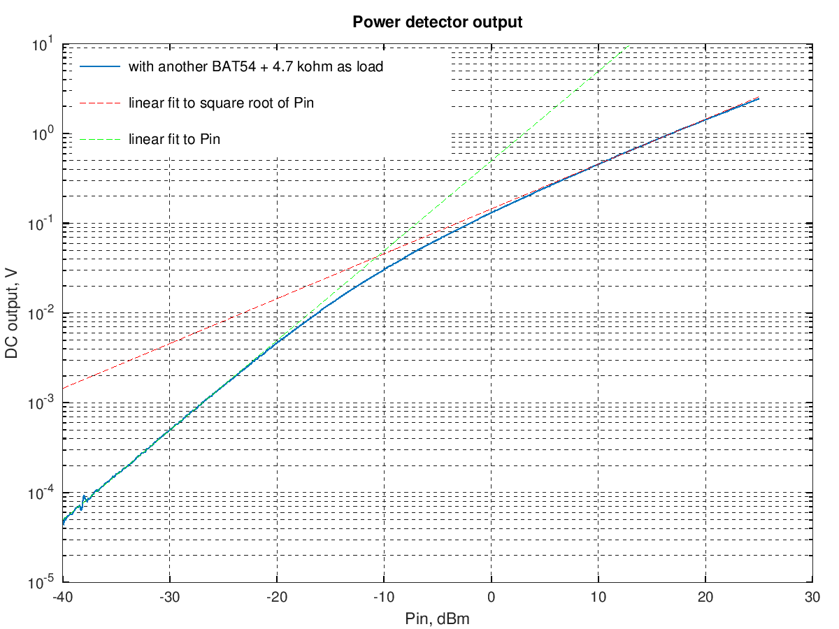
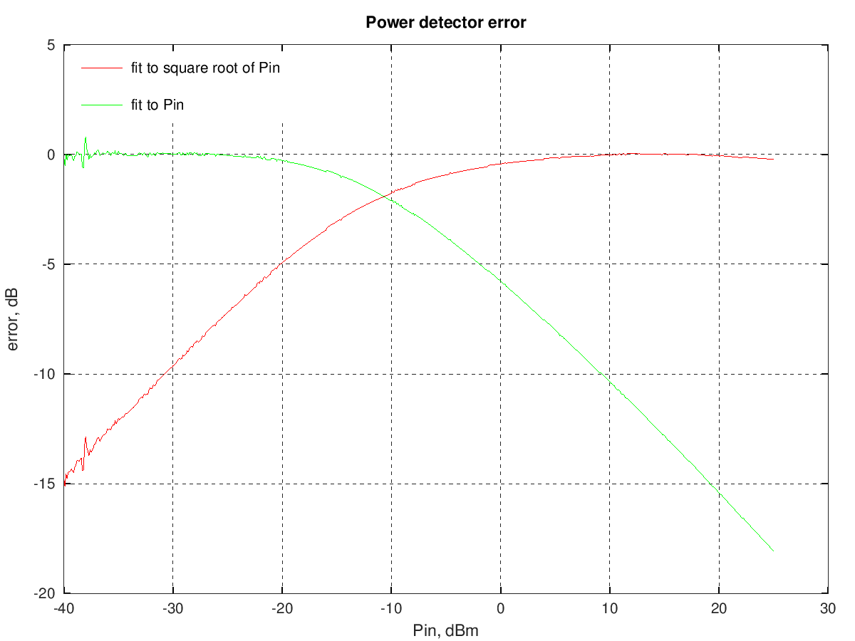
As for the previous circuit, the low-power fitting line was computed to minimize the fitting error between -40 dBm and -30 dBm and the high-power one to minimize the error between 9 dBm and 19 dBm.
The fitting error for these two lines is shown in the following graph:
Using a plain silicon diode
A a plain silicon diode (non-Schottky) has a much lower saturation current, so would need an even higher load to have a nice linear response.
At high input power the output still becomes proportional to the input peak voltage but at low input levels the output is quite lower than for a Schottky diode:
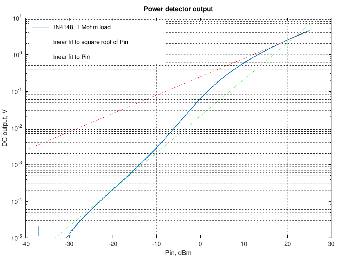
The low-power fitting line was computed to minimize the fitting error between -25 dBm and -15 dBm and the high-power one to minimize the error between 15 dBm and 25 dBm.
In the intermediate region a greater-than-square-law slope is seen; this is well analyzed in [4].
References:
| [1] | John Grebenkemper, "The Tandem Match - An Accurate Directional Wattmeter," QST, Jan 1987. |
| [2] | Hans Eriksson and Raymind W. Waugh, "A temperature compensated linear diode detector," RF Design, Jun 2000. |
| [3] | "A Temperature Compensated Linear Power Detector," Application Note 1328, Avago Technologies. |
| [4] | R. G. Harrison and X. Le Polozec, "Nonsquarelaw behaviour of diode detectors analysed by the Ritz-Galerkin method," IEEE Trans. Microwave Theory Techniques, vol. 42, no. 5, pp. 840-846, May 1994. |