Phase Locked Loop Theory
Understanding the functionality of the Phase Lock Loop frequency synthesiser is key to re-adjusting these radios. I am indebted to the guys on the UK Vintage Radio Repair and Restoration Forum for guiding me through this process. More...
Frequency generation in the Zycomm is performed by a Phase locked loop Circuit.
In fact, a “Dual Modulus” Phase Locked Loop circuit.
Initially, My knowledge of these was fairly sketchy on this topic, and searching on Google generally resulted in lots of learned PhD papers full of calculus - relating to such aspects as stability, lock-in performance, etc - none of which were really necessary for our attempt to tweak the radios slightly.
To cut a long story short, after a lot of reading, head scratching, and chatting on the Vintage radio forum, here’s my take on it. Before reading on have a look online for basic PLL theory. (and I mean basic - try YouTube)
Then, have a read of this Wikipedia article (which I corrected).
https://en.wikipedia.org/wiki/Dual-modulus_prescaler
To summarise a bit:
A dual modulus prescaler chip is used in high-frequency synthesizer designs to overcome the problem of generating narrowly spaced frequencies that are too high to be passed directly through the feedback loop of the system. A dual-modulus prescaler is a high-frequency divider with two separate frequency divisors, usually called M and M+1. More of that later.
A frequency synthesizer produces an output frequency, fo, which, divided by the modulus, N, is the reference frequency, fr:
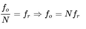
Typically, the possible frequency multiples will be the channels for which the radio equipment is designed, so fr will usually be equal to the channel spacing - on narrow-band radiotelephones, a channel spacing of 12.5 kHz is typical.
A problem now arises -if the programmable divider, using N, is only able to operate at a maximum clock frequency of, say, 10 MHz, but the output fo is required to be in the hundreds of MHz range, we must interpose a fixed prescaler (divider) that can operate at this frequency range. This has a division ratio M. If we insert a prescaler with, say M=40, this drops the frequency down into a range suitable for the programmable divider chip. But the output frequency is now:
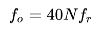
So, if fr remains at 12.5 kHz, only every 40th channel can be obtained, because every time N jumps by 1 count, the output frequency will increase by 40 x the channel spacing (fr).
The solution is the dual modulus prescaler. To operate this, the main divider is split into two parts, the main part N and an additional divider A, which is always less than N. This now works as follows:
Both dividers are clocked from the output of the dual-modulus prescaler, but only the output of the N divider is fed back to the phase comparator. Initially, the prescaler is set to divide by M + 1. Both N and A count down until A reaches zero, at which point the prescaler is switched to a division ratio of M. At this point; the divider N has completed A counts. Counting continues until N reaches zero, which is an additional N - A counts. At this point, the cycle repeats. Here’s the maths:

And so, having worked this out, the Motorola MC145146 data sheet started to make sense – and what the guys on the Vintage radio forum were explaining also became clearer.
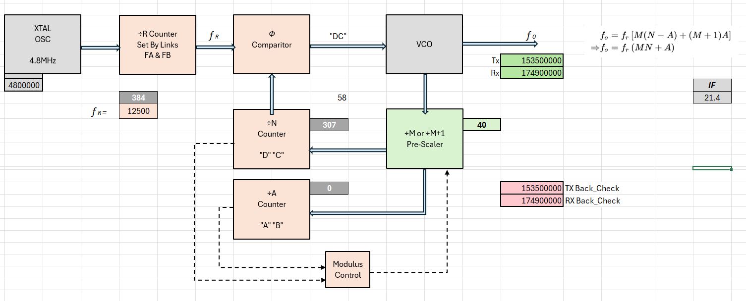
Additionally, a further point to note is that reference frequency (fr) is derived from a crystal oscillator (this is not the VCO). This crystal oscillator is divided by “R” before it is fed to the Phase comparator.
In Summary
N= the main divider modulus
A= the auxiliary divider modulus – used to swap the pre-scaler
M= the prescaler modulus (a value fixed in the chip)
R= the reference divider modulus ( which also sets the minimum channel spacing)
Having previously created some spreadsheets to calculate the correct bytes (to put into the Eeprom to alter the tuning), I could now take these hexadecimal values and determine the values of the Moduluses - (is it Moduli ?) for all three: R A and N. (remember M is fixed to 40 by the prescaler chip)
And having established these numbers, I was then able to stuff to the results into the above equation and thereby perform a “back check” - ensuring the bytes would produce the desired frequencies.
Motorola MC145146 System
This chip has three registers that need to be loaded from the Eprom, [ R,A,&N ]
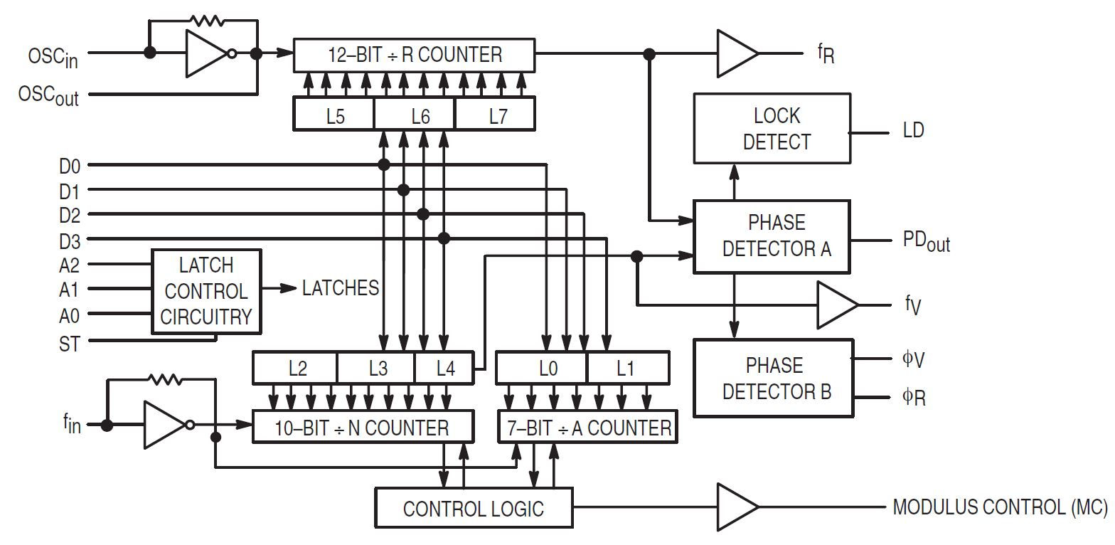
The bytes loaded in are confusingly called “L” in the datasheet, but we’ll stick with “D”
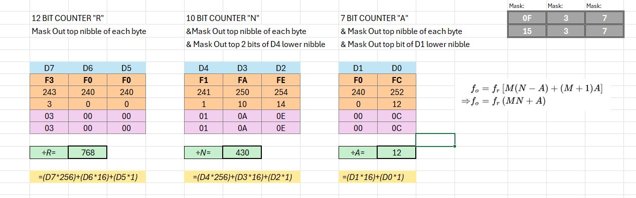
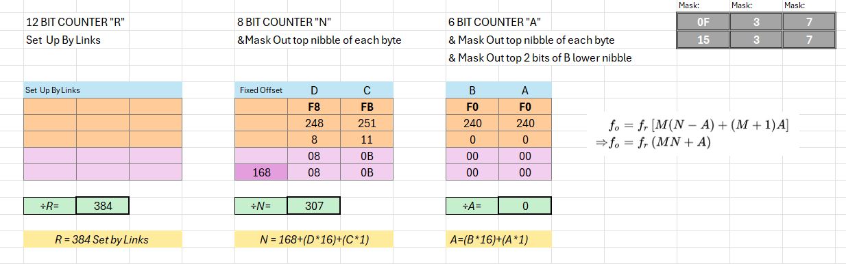
The above snip of the Motorola spreadsheet demonstrates an example of a typical loading of 8 bytes. To find the Modulus, each byte is first processed to mask undesired bits and then the decimal value of the lower nibble extracted. From this the Modulus number can be calculated (formulas in the Yellow Boxes)
Below is a diagram of the complete Motorola PLL system. The beige boxes show functions inside the MC145146. The green box is the Plessy SP8793 pre-scaler chip.
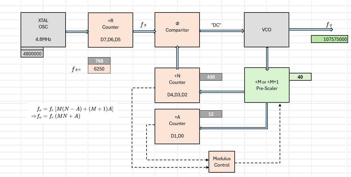
The small white numbers are the Modulus values from the previous diagrams. Feeding these into the formula results in the VCO running at 107.575MHz. (Note: This is just some random stuff – not a set pulled from the original Eproms)
Plessey System
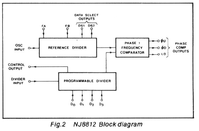
This is a truly horrible thing to understand. Some of the features are selected by hard-wired links and so need to be determined from the PCB layout. The Datasheet is very confusing as to the purpose of the four bytes, ie which are controlling the N and A modulus.
No clues in the block diagram:
Determining the channel spacing (fr) is done using the chart below and inspecting the PCB - but to get the R divider value requires a calculating: the crystal frequncy divided by fr..

In this chip, the R modulus is selected by linking some of the pins of the NJ8812 together
Annoying, there is a fixed value added to calculate the N modulus. This value is cunningly disguised in the Plessey Data sheet and took quite some time and effort to establish. The datasheet only gives the overall divide ration of the NJ8812 and the SP8793 pre-scaler combined. Furthermore, there are two options for this selected by another link.
The above snip of Plessey spreadsheet demonstrates an example of a typical loading of 4 bytes. To find the Modulus, each byte is first processed to mask undesired bits and then the decimal value of the lower nibble extracted. From this the Modulus number can be calculated (formulas in the Yellow Boxes)
Below is a diagram of the complete Plessey PLL system. The beige boxes show functions inside the NJ8812. The green box is the Plessy SP8793 pre-scaler chip
As above, the small white numbers are the Modulus values from the previous diagram. Feeding these into the formula results in the VCO running at 153.5MHz. (Note: This is just some random stuff – not a set pulled from the original Eproms)
In conclusion, I would have never understood the Plessey system, unless I had first taken the time to work my way through the Motorola Chip.