Phase Locked Loop Part 2
Understanding the functionality of the Phase Lock Loop frequency synthesiser is key to re-adjusting these radios. I am indebted to the guys on the UK Vintage Radio Repair and Restoration Forum for guiding me through this process.More...
This section was written after our initial investigations, as outlined in Testing session 1, where we discovered the second radio had a different PLL chip, and that the Eprom programming was different
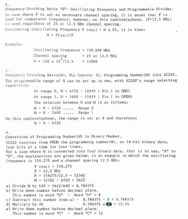
The attached manual
extract details the content of the Eprom bytes used with the Plessy NJ8812 . As
before, we can ignore the CTCSS side of things, as there is a 3rd party board
fitted for that function.
The mechanism by which the bytes are constantly written into the PLL chip from
the Eprom differs from the Motorola chip. The Plessey system uses address bits
derived from the refence divider within the PLL chip. These form a circulating
2 bit counter controlling the two lowest address lines on the Eprom. So, in
this system the PLL “pulls” the data from the Eprom.
From the schematic we can see that the A2 will changes when the set goes from RX to TX and back - A2 is high on Tx. This al means that there are 4 bytes per Tx or Rx setting.
Since A2 does follows the PTT state then the characters in the EPROM look like this:
Bytes 0 to 3 Channel 1 RX frequency (only lower nibble used)
Bytes 4 to 7 Channel 1 TX frequency (only lower nibble used)
Bytes 8 to 11 Channel 2 RX frequency (only lower nibble used)
Bytes 11 to 15 Channel 2 TX (frequency (only lower nibble used)
...and so on all the way up to channel 16 - because the code applied by the channel switch to the EPROM A3-A6 is 4-bit.
Once again, I focussed on one group of 8 bytes. As with the Motorola PLL, within each byte only one nibble is used - as the PLL only has a four-bit data bus. Also, as seen in the manual’s example, the upper nibble has all bits set to “1”s – ie “F”. So, this should result in Eprom bytes containing values such as F0, FC etc
As with the Motorola PLL previously discussed, I worked though the example calculation methodology from the manual, by means of a spreadsheet. This very rapidly got confusing due to the odd loading order of the four bytes, and identifying how the four byes controlled the division modulus within the PLL chip.
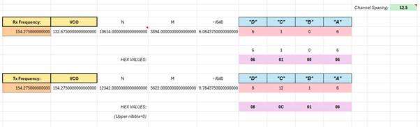
As before, I expanded my spreadsheet idea - so that it works in reverse – allowing me to enter the bytes read from the Eprom and back calculate what the TX and Rx frequencies would be
This is how the Zycomm manual explains how to derive the correct bytes to load into the Eprom. The NJ8812 has some pretty strange, fixed offsets and constants in the calculations, due to the way the dividers are designed. There is a bit more on this in the section on PLL theory.
There is another similar description in the datasheet for the NJ8812