HT220
Frequency Synthesizer
originally published
1976
by Dale Heatherington, WA4DSY
edited for webpage use by Michael Wright, KG6BFK
http://www.geocities.com/mikeht220/220synthesizer.html
Introduction
The
following instructions pertain to the new board marked with the number 051776.
There have been several improvements made over the old board. Most noteable
is the reduction of receiver birdies and a 12 mA reduction of the power drain.
Only 2 receiver birdies remain; 146.000 and 147.100 MHz. The transmitter spurious
outputs are at least 5 dB better and the broad band white noise is down much
more, The white noise reduction also resulted in improved receiver sensitivity.
I still don’t recommend using a high power amplifier with the synthesized HT220
but if you feel the need to do so here is the formula to compute the 2 major
spurs so you will at least know where your QRM is,
|
Upper
spur =
|
F
+ ((F/9) - 15.5555) for simplex
|
|
|
F
+ ((F/9) - 15.4888) for -600 KHz
|
|
|
F
+ ((F/9) - 15.6888) for +600 KHz
|
|
|
|
|
Lower
spur =
|
F
- ((F/9) - 15.5555) for simplex
|
|
|
F
- ((F/9) - 15.4888) for -600 KHz
|
|
|
F
- ((F/9) - 15.6888) for +600 KHz
|
|
|
|
|
|
where
F = operating frequency in MHz
|
|
|
|
|
example:
|
F
= 146.520 MHz simplex
|
|
|
lower
spur = 145.796
|
|
|
upper
spur = 147.244
|
Another
major improvement was the elimination of the two CD4011 ICs. Many people found
it was hard to find CD4011s that would work right in the original circuit. That
is no longer a problem since there are no CD4011s in the new circuit. Some people
have ask why I used 9.10222 MHz for the reference frequency instead of 4.551111
MHz so the CD4020 reference divider would not be pushed to it’s limit. The answer
is simple.... High accuracy crystals in the HC 18/U holder below 6 MHz are not
available.
A
word about IC sockets: You can use low profile sockets if you bond the leads
that need to be soldered to the top side of the board out to the side so you
can solder to them. Be careful that they don’t touch anything they should not.
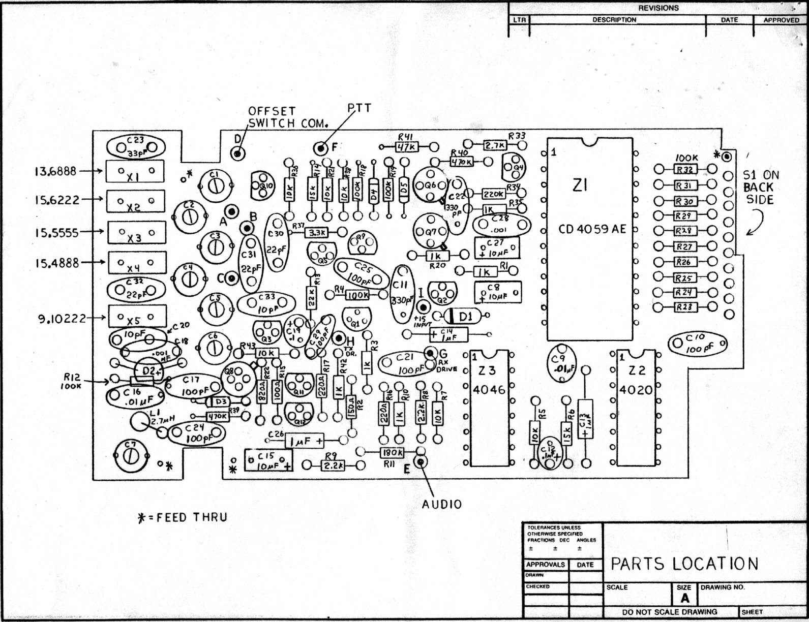
Drawings
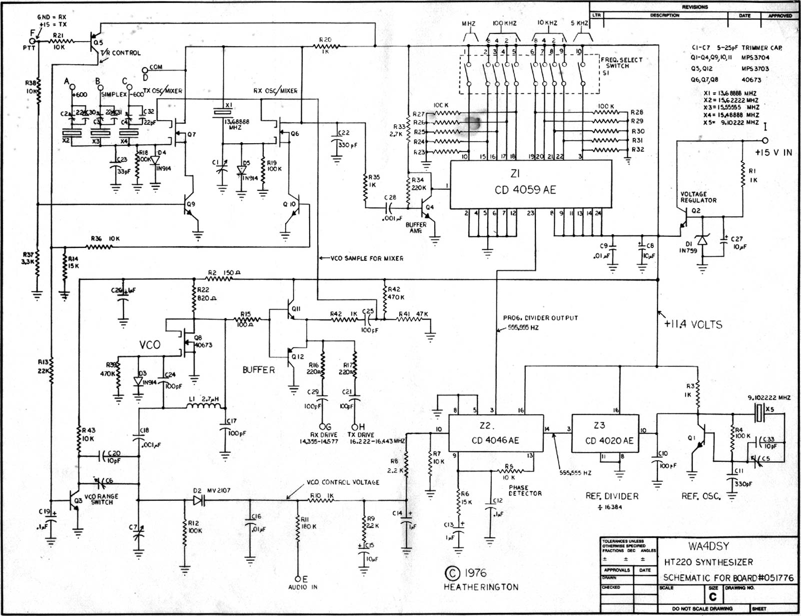
Parts List
|
|
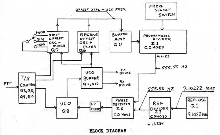
| Z1 |
CD4059AE |
Programmable
divider |
| Z2 |
CD4046AE |
Phase look
loop |
| Z3 |
CD4020AE |
14 stage divider |
Q1, Q2, Q3,
Q4, Q9, Q10, Q11 |
MPS3704 or
2N4401 |
NPN transistor |
| Q5, Q12 |
MPS3703 or
2N4403 |
PNP transistor |
| Q6, Q7, Q8 |
40673 |
RCA dual gate
MOS-FET |
| D1 |
1N759 |
or any 12
volt 400mw zener diode |
| D2 |
MV2107 or
MV2106 |
Motorola EPICAP
tuning diode (22pF at 4V) |
| D3, D4, D5 |
1N914 or 1N4148 |
diode |
| S1 |
76A10 |
Grayhill 10
unit DIP switch |
R1, R3, R10
R20, R35 |
1000 ohm |
1/4 watt 5%
resistor |
| R2 |
150 ohm |
1/4 watt 5%
resistor |
R4, R12, R18,
R19, R21, R24,
R25, R26, R27,
R28, R29, R30,
R31, R32 |
100K ohm |
1/4 watt 5%
resistor |
R5, R7, R18,
R21, R36, R38 |
10K ohm |
1/4 watt 5%
resistor |
| R6, R14 |
15K ohm |
1/4 watt 5%
resistor |
| R8, R9 |
2.2K ohm |
1/4 watt 5%
resistor |
| R11 |
180K ohm |
1/4 watt 5%
resistor |
| R13 |
22K ohm |
1/4 watt 5%
resistor |
| R15 |
100 ohm |
1/4 watt 5%
resistor |
| R16, R17 |
220 ohm |
1/4 watt 5%
resistor |
| R22 |
820 ohm |
1/4 watt 5%
resistor |
| R33 |
2.7K ohm |
1/4 watt 5%
resistor |
| R34 |
220K ohm |
1/4 watt 5%
resistor |
| R37 |
3.3K ohm |
1/4 watt 5%
resistor |
| R39, R40 |
470K ohm |
1/4 watt 5%
resistor |
| R41 |
47K ohm |
1/4 watt 5%
resistor |
| C1-C7 |
5-25 pF trimmer |
Erie 518-000-5-25
or equivalent
size: 0.220" dia. x 0.170" high |
| C8, C15, C27 |
10 uF at 20
VDC |
Sprague 183DR106X002D
or equiv.
sub-miniature tantalum capacitor (radial leads) |
| C9, C16 |
0.01 uF at
100 VDC |
Disc ceramic
capacitor (0.300" max dia.) |
C10, C17,
C21
C24, C25, C29 |
100 pF |
Disc ceramic
capacitor (0.300" max dia.) |
| C11, C22 |
330 pF |
Disc ceramic
capacitor (0.300" max dia.) |
| C20 |
10 pF |
Disc ceramic
capacitor (0.300" max dia.) |
| C23 |
33 pF |
Disc ceramic
capacitor (0.300" max dia.) |
| C30, C31,
C32 |
22 pF |
Disc ceramic
capacitor (0.300" max dia.) |
| C18, C28 |
0.001 uF |
Disc ceramic
capacitor (0.300" max dia.) |
| C33 |
10 pF |
Disc ceramic
capacitor (0.300" max dia.) |
| C12, C19 |
0.1 uF at
35 VDC |
Sprague 182DR104D4035H
or equiv.
Sub-miniature tantalum capacitor (radial leads) |
| C13, C14,
C26 |
1 uF at 25
VDC |
Sprague 16D105X9025BC2
or equiv.
Sub-miniature tantalum capacitor (axial leads) |
| L1 |
2.7 uH |
2.7 micro
henry choke or
40 turns of #36 magnet wire
wound on the body of a 1 meg ohm
1/2 watt carbon resistor. |
| X1 |
13.68888 MHz |
crystal |
| X2 |
15.62222 MHz |
crystal |
| X3 |
15.55555 MHz |
crystal |
| X4 |
15.48888 MHz |
crystal |
| X5 |
9.10222 MHz |
crystal |
Crystals are 0.002%,
20 pF load cap. calibrated at room temp. HC 18/U holder. Order type HA-M1 from
International Crystal Mfg Co. http://www.icm.com/
Specifications
Frequency range:
146.000 to 147.995 MHz transmit and receive
Channel spacing:
5 KHz
VCO frequency
Transmit 16.2222
- 16.4438 MHz
Receive 14.3555 - 14.5772 MHz (for 16.8 MHz rec. IF)
Power requirements:
12 to 15 volts at at 29 mA
Spurious outputs:
45 dB below carrier
Transmitter offsets
for repeaters: -600 KHz, +600 KHz, and simplex
Input/Output lead
description
- to +600
KHz lug on transmit offset switch
- to simplex
lug on transmit offset switch
- to -600
KHz lug on transmit offset switch
- to common
lug on transmit offset switch
- Audio
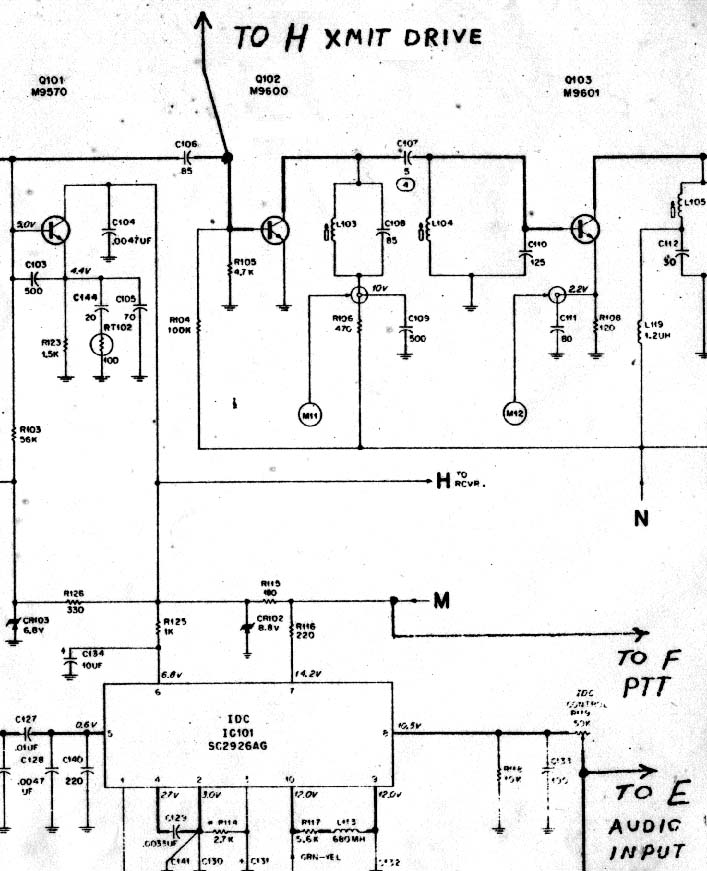
input. Connect to wiper of the IDC control in the HT 220.
- PTT (+14.6
transmit, gnd for receiver. Connect this lead to point M in the transmitter
power distribution circuit of the HT 220.
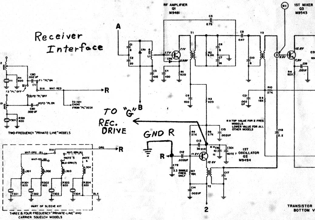
- VCO drive
for the receiver. Connect to emitter of receive 1st osc. transistor. *
- VCO drive
for the transmitter. Connect to base of 1st tripler transistor. *
- Power
input from battery.
GND.
Connect a wire between the synthesizer ground and the HT 220 ground.
*
See interface diagrams for details
Construction
Hints
Because of the
high parts density of this circuit, the procedures outlined below should be
followed.
- Use a low wattage soldering iron with
a small tip and #24 or smaller gauge solder.
- Since the holes in the circuit board
are not plated thru, you must solder the narts on both the top and
bottom of the board where necessary.
- The order in which the parts are installed
is important because some parts overlap others. Install all the feed-thru
wires first. Next install the dip-switch on the bottom of the board and solder
it in place. Be sure it will be right side up when the board is installed
in the radio. Put in all of the transistors next. Q1, 3, 4, 8, 9, 10 and 12
need one or more leads soldered to the top of the board. The remaining parts
can be installed in any order but the three ICs should be put in last. IC
sockets can NOT be used because some pins need to be soldered on top of the
board.
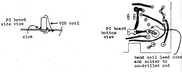
- The VCO coil is a 2.7 uH inductor.
You can wind it yourself if you prefer.
- Select 1/2 watt carbon
resistor greater than 1 meg-ohm with a straight smooth body.
- Cut a shallow notch in
each end with a triangle file as illustrated.
- Cut a 19 inch piece of
#36 magnet wire and remove 1 inch of insulation from each end.
- Wind 40 turns close spaced
in a single layer on the resistor body and solder both ends of the coil
to the resistor leads.
- Coat the finished coil
with lacquer to secure the windings.
- Install the coil on the
circuit board as illustrated below.
- The transmit offset switch is a 3
position rotary switch that replaces the original "PL" switch. Some PL switches
can be modified for 3 positions by removing a stop in the switch. Check the
top of your switch for a pin which could be moved or removed.
- The synthesizer can only be installed
in the long omni housing with the privateline board and all other accessories
removed. The extention sleeve must be modified by cutting out the antenna
sheath and all other mounting tabs around the edges. The antenna cannot be
fully collapsed when the synthesizer is installed. A rectangular hole must
be out in the back for the frequency select switch. These modifications can
be done with an Xacto knife and a mototool.
- Wiring between the radio and the synthesizer
should be done with #26 or #28 gauge stranded wire.
- The parts near the VCO coil should
be glued down to prevent vibration from modulating the VCO.
Test and Alignment
Test equipment needed:
- 20 MHz frequency counter
- 15 volt 100 mA DC power supply
- VTVM
Note: It is better to do preliminary
test and alignment before you connect the synthesizer to the radio. It can prevent
trouble later on if you locate any "bugs" now.
Reference oscillator adjustment
- Connect 15 volts to the board. + to
point I, - to the ground foil.
- Connect the frequency counter lead
thru a 20 pF capacitor to pin 10 on Z3, the CD4020.
- Adjust C5 for 9.10222 MHz.
VCO and offset oscillator adjustments
- Connect the frequency counter lead
to point H (xmit drive).
- Connect the VTVM to the + side of
C14 (1 uF).
- Set S1 (freq. select switch) to 147.000
MHz.
- If the board is not in the radio,
connect point F (ptt) to +15 volts. This puts the synthesizer in transmit
mode. If the board is in the radio you must key the transmitter.
- Connect a temporary jumder wire from
point D to point B. This puts the synthesizer in simplex mode.
- Turn on the power and adjust C7 for
a 5 volt reading on the VTVM. If you get the 5 volt reading at this time all
of the circuits are working ok.
- Adjust C3 for 16.33333 MHz VCO frequency.
- Remove the jumper from point b and
connect it to point A. This puts the synthesizer in +600 KHz mode. Adjust
C2 for a VCO frequency of 16.4000 MHz.
- Remove the jumper from point A and
connect it to point C. This puts the synthesizer in -600 KHz mode. Adjust
C4 for a VCO frequency of 16.26666 MHz,
- Remove the jumper from point P to
+ 15, Connect the jumper from point F to ground. This puts the synthesizer
in receive mode.
- Adjust C6 for a 5 volt reading on
the VTVM. Adjust C1 for a VCO frequency of 14.4666 MHz.
Alignment is now complete and the synthesizer
can now be installed. In the radio, some of the trimmer capacitors may need
to be touched up after it is in the radio. Below is a list of the trimmers and
their function,
C1 Receive Frequency
adjust
C2 +600 KHz offset frequency adjust (transmit)
C3 Simplex frequency adjust (transmit)
C4 -600 KHz frequency adjust (transmit)
C5 Reference oscillator frequency adjust
C6 VCO range adjust (receive)
C7 VCO range adjust (transmit)
NOTE: If you have trouble with any of
the test and alignment steps cheek for a 555.555 Hz square wave at pin 3 on
Z3, CD4020. Some 4020s won’t work at 9.1022 MHz. If you have an input on pin
10 of this IC but no output on pin 3 you need to try another one.
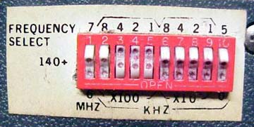
How to use the binary frequency select
switch
This switch consist of 10 spst switchs
numbered 1 thru 10. In the following discussion an "ON" switch will be called
1 and an "OFF" switch will be called 0. The frequency is entered directly in
BCD code.
Switch #1 is the MHz select switch: 0
= 146.XXX MHz, 1 = 147.XXX MHz
Switches #2, 3, 4, 5 are the 100 KHz
select switches. They are BCD coded and can select any digit from 0 to 9.
Switches #6, 7, 8, 9 are the 10 KHz select
switches. They are also BCD. coded and can select any digit from 0 to 9.
Switch #10 is the 5 KHz select switch.
0 = 14X.XX0, 1 = 14X.XX5
Note: The following is in courier font
so the numbers should align in proper columns.
BCD code for
switches 2 thru 9
BCD code, 0 = off, 1 = on
Switch number
2 3 4 5 or
6 7 8 9
-------
0 0 0 0 = 0
0 0 0 1 = 1
0 0 1 0 = 2
0 0 1 1 = 3
0 1 0 0 = 4
0 1 0 1 = 5
0 1 1 0 = 6
0 1 1 1 = 7
1 0 0 0 = 8
1 0 0 1 = 9
-------
8 4 2 1 = binary weight
Examples:
MHz 100
KHz 10 KHz 5 KHz
1 2 3 4 5 6 7 8 9 10 switch
number
0 0
0 0 0 0 0 0 0 0 = 146.000
0 0 1 0 1 0 0 1 0 0 = 146.520
0 1 0 0 1 0 1 0 0 0 = 146.940
0 1 0 0 0 0 0 1 0 0 = 146.820
1 0 0 0 0 0 0 0 0 0 = 147.000
1 0 1 1 1 0 0 1 1 1 = 147.735
Caution, when operating
above 147.400 MHz be sure the transmit offset switch is in simplex or -600 KHz.
If not the transmitter will transmit at 148 MHz or above.
Photo of DIP
switch in back of a HT220 (image from a eBay item)
Feedback is desired
(suggestions, comments, errors, gripes, whatever) Michael Wright, KG6BFK, [email protected]

[ About me
| Acronyms | CW
| Data Sheets | Docs
| Download | E-mail
| HOME | Ham
projects | Hobby circuits
| Photo galery | PIC
| QTH
photos |
Sign
in my guestbook | View
my guestbook ]
© 2001 - YO5OFH, Csaba Gajdos
