13.8 V / 15 A from a PC Power Supply
Safety Instructions
Caution mortal danger: The following circuit operates at a mains voltage of 230 Vac. Because of rectification some of the components conduct dc voltage of more than 322 V. Work has to be carried out only if the circuit is disconnected from the mains and de-energized. Note that capacitors located to the primary side can be charged with high voltage for several seconds even after switching of the mains voltage.
The major disadvantages of usual linear power supplies are high power dissipation, the size and the appropriated weight. When looking for an alternative solution, I decided to use a switch mode power supply (SMPS). The efficiency of such power supplies is around 70 % to 90 % at a power density of 0.2 W / cmł. Because homebrewing was out of the question due to lack of time, I tried the modification of a PC switch mode power supply.
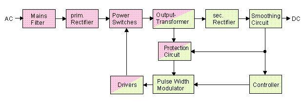
Fig.1: Block diagram of a primary
switching power supply
Brief description of PC SMPS Features
Depending on the PC model, these are rated anywhere between 150 and 240 W. For supplying socket 7 main boards they have four different output voltages of +5 V, +12 V, -12 V and -5 V. They are mainly primary switching power supplies with power switches arranged in a half-bridge configuration. The outputs can drive the usual 20 A (+5 V), 8 A (+12 V) and 0,5 A (-12 V, -5 V). At approx. 205 W output power and a typical efficiency of 75 % this means a dissipation of only 68 W. I had acquired an unbranded PC power supply, measuring 140 x 100 x 50 mm (W, D, H) and weighing 350 g. Most power supply units are designed according to the same principle (half-bridge configuration) and hence the following described modification should be applicable also to power supplies from other producers.
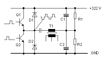
Fig.2: Half-bridge configuration of power switches
Regulation
After switching on the mains voltage
the circuit operates for a short duration as a free-running oscillator. This
behavior is caused by a feedback winding at the output transformer T2. As soon
as the auxiliary voltage Uaux is present the pulse width modulator IC TL494CN
from Texas-Instruments takes over the control function and synchronizes the
"oscillator".
The error amplifier in the TL494 compares the voltage at the +5 V output (actual
value) with a reference voltage (set value), calculates the analogue control
variable according to the PI algorithm and adjusts the pulse width modulator
(see Fig. 6). The modulator sends alternate pulses to the driver transistors
Q5 and Q6. The pulse duration is reverse proportional to the control variable
rating. Increasing loading on the +5 V output makes for wider pulses, lighter
loading causes narrower pulses. As there is a finite minimum pulse width, a
minimum load of 0.1 A is required. Without this load the power supply may be
destroyed. The switching frequency is approx. 33 kHz as usual for PC power supplies.
It is defined by a resistor and a capacitor located at pin 5 and 6 of IC1.
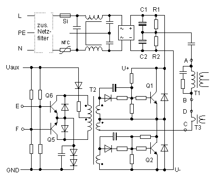
Fig. 3: Primary side mains filter,
rectifier, power switches and drivers
Monitoring Circuit
Several protection circuits are included in the
original power supply. Excessive primary current due to a very high secondary
current leads to a high alternating voltage at the T3 output. If this voltage
is above a fixed threshold the TL494 stops immediately generating cyclically
pulses and changes to the intermitted mode (on / off). The circuit and the load
are protected likewise against over-voltage at the +5 V output or short-circuit
at the -12 V and -5 V outputs. Switching off is executed via H-signal to the
IC1 protection input (pin 4) too.
If you see a KA7500 or IR3MO2 PWM regulator IC on the board, each one is a pin
compatible second source to the TL494CN. IC3 is a dual comparator from LM339
type. Some power supplies are not equipped with this IC, but with a two transistor
discrete monitoring circuit, offering the same functionality.
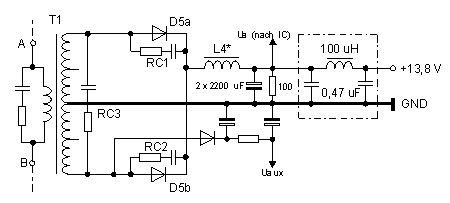
Mods to the Secondary Rectification
The intent is for all of the available
power at the 12 V secondary of T1 to be rectified, regulated, protected and
filtered to provide a single output of 13.8 V DC at 205 W, or more if possible.
A first check indicates that the +12 V wire was of the same diameter as the
+5 V wire.
First unsolder and remove all components on the secondary side of T1 which are
provided for rectification, filtering and regulation of the four output voltages.
On that part of the board are only remaining three RC members RC1 to RC3 and
the components for providing the auxiliary power supply Uaux.
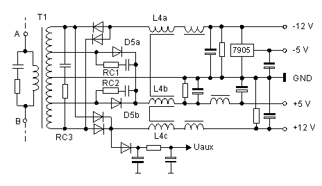
Fig.4: Secondary rectification as found in
the original PC power supply
Reconstruction of the secondary side.
| Break the PCB tracks between the RC members RC1 / RC2 and both 5 V taps of the T1 secondary winding. |
| Modify L4 for 12 V at 20 A. Remove windings L4a, L4b and L4c from the toroid (counting turns of L4c). Rewind the toroid L4* with a single winding, turn count as old L4c but with 2.5 times the thickness. Take two wires with 1 mm diameter each, bifilar wounded. |
| Install two low ESR electrolytic capacitors of 2200 uF each and the 100 Ohm bleeder resistor as permanent load. |
| Use the old PCB tracks from the +5 V section and GND tracks as terminals for L4* , the 100 Ohm resistor and the two 2200 uF capacitors. Insert L4* at the same place onto the PCB component side where the L4b winding was connected before. |
| The original cooling of the rectifier diode D5 is insufficient. Adequate cooling is achieved by a finned heat sink measuring 70 x 50 x 30 mm (W, D, H) instead of the old aluminium sheet metal. |
| Fasten D5 to the heat sink and extend the three leads by 40 mm long wires. Use isolation material and thermal compound. D5 carries on some boards the abbreviation SKD. |
| Place the finned heat sink approx. 40 mm above the "stripped" secondary (see photo) with plastic spacers and long M3 screws (avoid short-circuit to common). |
| Connect the anode leads of D5a and D5b with one RC member RC1 / RC2 each. The cathodes have to be connected to the nodal point of RC1, RC2 and L4. |
| Establish two links between the 12 V terminals of T1 and the RC members by two thick wires. D5 will be fed from the 12 V winding. |
A simple and clear structure of the secondary rectification was achieved after "stripping" and "reconstruction".
Fig. 5: New designed secondary
for Ua = 13,8 V
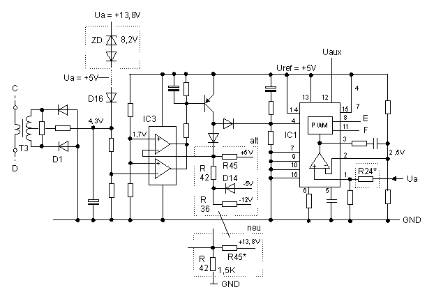
Mods to the Regulation and Protection Circuit
The part of the circuit responsible for regulation and monitoring has to be modified at three places. Arrange additional components free standing onto the component side of the PCB.
| R24* is calculated for 13.8 V output voltage.
The voltage at the (+) input of the error amplifier must be equal to 2.5
V after control loop stabilization, i.e. half the 5 V reference voltage
when the output is at 13.8 V. R24* = 20 kOhm = 2 x 10 kOhm in series |
| Arrange a second universal diode 1N4148 and
a 8,2 V Zener diode in series to D16. Usum = 8,2 V + 2 x 0,7 V = 9,6 V |
| Simplify the voltage divider (R36, R42, R45
and D14) in the short-circuit protection circuit. For this remove R36 and
D14. Connect the free end of R42 to common (GND) and replace R45 with one
of higher value to ensure no shut-down at normal operation. The voltage
across R42 must be less than 1,7 V (I chose 1,2 V). R45* = 15 kOhm |
The areas marked with dotted frames, show the modified or additional components that are necessary for 13.8 V output voltage.
Fig. 6: Regulation and protection circuits
incl. all modifications
Further Modifications
After commissioning the modified board, the situation regarding to interferences looks very bad. The whole reception range from 3,5 MHz to 30 MHz was disturbed by harmonics of the 33 kHz switching frequency. S-meter readings showed S5 on 80 m down to S2 on 10 m. As I was testing the board in a metal box, the HF radiation could only get out on the mains cable and/or DC output leads. The insertion of an additional standard 230 VAC mains filter and a home-brewed pi-filter in the output rendered the interference inaudible.
| Insert an additional 230V / 2A mains filter to the primary side, close to the place where the mains cable enters the enclosure rear wall. |
| Insert a 20 A pi-filter to the DC output , behind the +/- DC terminals at the rear wall. |
| The power supply enclosure must absolutely consist of iron sheet metal to screen magnetic fields. Aluminum plates protect only against electrical fields. |
| Optional on the primary: Replace the 220 uF smoothing capacitors C1 and C2 by 470 uF capacitors. This reduces primary ripple, which helps output regulation at full load. |
Testing the Power Supply
Phase 1: These tests have to be carried out at a low DC supply voltage in order to avoid component destruction in case of possible errors. The 13.8 V output is loaded with a 12 V / 50 W car headlight bulb and a 15 V / 1 A lab power supply is connected to GND and Uaux. The TL494 IC gets its operating voltage and generates control pulses with maximum pulse duration. Check the signals at Q5 and Q6.
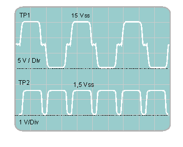
Phase 2: During the second test phase the galvanic isolated primary side of the circuit is supplied by the lab supply too. For this purpose make a short cable link between Uaux and U+ as well as between GND and U-. The PWM controller tries to offer 13.8 V at the output at maximum pulse duration. The later cannot be successful due to the low 15 Vdc input voltage and the present transformer ratio. With an oscilloscope measured signals at the measuring points TP1 (emitter Q1 against emitter Q2) and TP2 (cathode D5 against GND) must look like as shown in figure 7.
Fig. 7: Signal shape at TP1 and
TP2
Phase 3: Nor disconnect the lab supply from the primary side only. Instead connect a 48 V / 1 A mains transformer to the L1 and N terminal in order to feed the board with a galvanic isolated Ac voltage. 60 Vdc at C1 and C2 is in Europe defined as a non-dangerous voltage rate. 48 VAC at the input causes a rise of the output voltage up to +6 V.
If everything is all right up to now, one can proceed with the exciting test at 230 Vac. The laboratory power supply, the 48 V transformer, the measuring instruments and all provisional cable links attached for the test etc. must obviously be removed. The car bulb are further needed as a load and for the functional checks. If after applying of the 230 Vac mains voltage the lamps light up brightly, the output voltage amounts to 13.8 V and no undefined noises or smells are noticeable one has won the first round. If a non recognizable error has passed the pre-testing the two switching transistors and copper tracks say good-bye with a more or less loud bang.
For the following load test some high power resistors with resistance 1 Ohm and sufficent power rating are required. The current flowing with this load should not cause excessive heating of the rectifier diode and the switching transistors during a 5 minutes test periode.
Warning: Check temperature of components only if the mains voltage is switched off
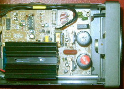
Cooling of the switching transistors Q1 and Q 2 at a continuos current of 15 A has to be improved in any case. When exchanging the small heat sinks, note that they form an electrical connection between coper tracks on some boards. Replace the missing connection by wire links. As one can see on the photo, I did not taken this measures for further power improvement.
Operation Experience
The modified board was permanently installed in the speaker cabinet SP120 that matches my transceiver. The mains lead exit from its back, which also carries the DC terminals, an on-off switch, the additional mains filter and a small 12 V blower. A green LED power-on indicator was inserted in the front panel into a 5 mm hole drill. I had installed the small blower just in case, but found it superfluous; at the low duty cycle of CW and SSB, none of the components is getting hot. The power supply has been used for several years and has given no problems.
Fig. 8: Modified power supply
board in the SP120 speaker cabinet
![]()
[ About me
| Acronyms | CW
| Data Sheets | Docs
| Download | E-mail
| HOME | Ham
projects | Hobby circuits
| Photo galery | PIC
| QTH
photos |
Sign
in my guestbook | View
my guestbook ]
© 2001 - YO5OFH, Csaba Gajdos