|
1 Second Time Base From
Crystal Oscillator
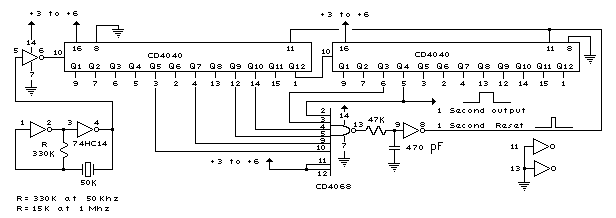
The schematic below illustrates dividing a crystal oscillator signal by the crystal frequency to obtain an accurate (0.01%) 1 second time base. Two cascaded 12 stage counters (CD4040) form a 24 stage binary counter and the appropriate bits are gated together to produce the desired division. Using a crystal of some even multiple of 2 is desirable so that one stage of the counter automatically toggles every second which eliminates the need for the NAND gate and reset circuitry, however the circuit below illustrates using a crystal which is not an even multiple of 2 and so requires additional components. Using a 50 Khz crystal, a count of 50000 is detected when the appropriate counter bits that add up to 50000 are all high. This corresponds to bits 15 (32768) + 14 (16384) + 9 (512) + 8 (256) + 6 (64) + 4 (16). Bits 14 and 15 are the 3rd and 4th stages of the second counter, bit 0 is the first stage of the first counter (Q1, pin 9). To use a 100 Khz crystal, each bit would be moved one to the right so the total would be (65536 + 32768 + 1024 + 512 + 128 + 32 = 100,000). Using a 1 Mhz crystal, the following bits would be needed: Bit 19 - Right counter - Q8 - pin 13 - Decimal value = 524288
18 7 4 262144
17 6 2 131072
16 5 3 65536
14 3 6 16384
9 - Left counter - 10 14 512
6 7 4 64
---------
1,000,000
At 1 Mhz, the 330K resistor in the oscillator circuit will need to be reduced proportionally to about 15K. When the terminal count is reached, a 7 uS reset pulse is generated by the Schmitt Trigger inverter stage that follows the NAND gate. The 47K resistor and 470 picofarad capacitor sustain the output so that the counters are reliably reset to zero. This is less than one clock cycle at 50Khz and does not introduce an error but would amount to 7 cycles at 1 MHz which would cause the counters to lose 7 microseconds of time per second. It's not much of an error (7 parts in a million) but it would be there. The minimum reset pulse width for the 4040 CMOS counters is about 1.5 uS, so the reset pulse cannot be made much shorter.
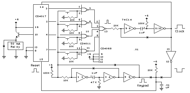
Digital Electronic Lock The digital lock shown
below uses 4 common logic ICs to allow controlling a relay by entering a 4
digit number on a keypad. The first 4 outputs from the CD4017 decade
counter (pins 3,2,4,7) are gated together with 4 digits from a keypad so
that as the keys are depressed in the correct order, the counter will
advance. As each correct key is pressed, a low level appears at the output
of the dual NAND gate producing a high level at the output of the 8 input
NAND at pin 13. The momentary high level from pin 13 activates a one shot
circuit which applies an approximate 80 millisecond positive going pulse
to the clock line (pin 14) of the decade counter which advances it one
count on the rising edge. A second monostable, one shot circuit is used to
generate an approximate 40 millisecond positive going pulse which is
applied to the common point of the keypad so that the appropriate NAND
gate will see two logic high levels when the correct key is pressed (one
from the counter and the other from the key). The inverted clock pulse
(negative going) at pin 12 of the 74C14 and the positive going kepad pulse
at pin 6 are gated together using two diodes as an AND gate (shown in
lower right corner). The output at the junction of the diodes will be
positive in the event a wrong key is pressed and will reset the counter.
When a correct key is pressed, outputs will be present from both
monostable circuits (clock and keypad) causing the reset line to remain
low and allowing the counter to advance. However, since the keypad pulse
begins slightly before the clock, a 0.1uF capacitor is connected to the
reset line to delay the reset until the inverted clock arrives. The values
are not critical and various other timing schemes could be used but the
clock signal should be slightly longer than the keypad pulse so that the
clock signal can mask out the keypad and avoid resetting the counter in
the event the clock pulse ends before the keypad pulse. The fifth output
of the counter is on pin 10, so that after four correct key entries have
been made, pin 10 will move to a high level and can be used to activate a
relay, illuminate an LED, ect. At this point, the lock can be reset simply
by pressing any key. The circuit can be extended with additional gates
(one more CD4011) to accept up to a 8 digit code. The 4017 counting order
is 3 2 4 7 10 1 5 6 9 11 so that the first 8 outputs are connected to the
NAND gates and pin 9 would be used to drive the relay or light. The 4
additional NAND gate outputs would connect to the 4 remaining inputs of
the CD4068 (pins 9,10,11,12). The circuit will operate from 3 to 12 volts
on 4000 series CMOS but only 6 volts or less if 74HC parts are used. The
circuit draws very little current (about 165 microamps) so it could be
powered for several months on 4 AA batteries assuming only intermittent
use of the relay.
Simple clock doubler +-------+
| hc86 |
+-----------| |
clkin ----+ | +--- clkout = 2*clkin
+-N-R-+-N---+ |
| | |
C +-------+
|
gnd
where N is a NOT gate (hc04?)
R is a 10k resistor
C is a 47pf capacitor.
The circuit functions quite well and is stable. If the Not gates are omitted,
however, it becomes unstable, and gives variable width pulses.
Divide and Multiply
The 2x trigger is a little involved, but here is a circuit that will do divide by two preserving pulse width. +5 ______
______ o______| \
In o___________________________| \ | \
| | \ | NAND )O__________o out
| | NAND )O_______| /
| ________| / |______/
| | |______/
| ______ |_________________
|__| \ ___________ |
| \ | | |
| NAND )O___|\ clk | |
+5 o____| / |/ Q |__|
|______/ | |
| _ |
____| D Q |__
| | | |
| | | |
| | D-type | |
| | Flip-Flop | |
| |___________| |
|___________________|
You can use a 74LS00 for the NAND gates and a 74LS74 for the flip-flop. Critter Ridder - Ultrasonic Sound Generator Legend: ) = No Connection
+ = Connection
All capacitors are 16V or more.
                 R2 same as R1              R1 1K to 10K
       +------------/\/\/\------------------+-----/\/\/\------+
       |                                    |                 |
       |     C1  .0015 uF                   |                 |
       |        ||                          |                 |
       +--------||-------------+            |                 |
       |        ||             |            |                 |
       |                       |            |                 |
       |       +---+-----------+            +-------+         |
       |       |   |           |            |       |         |
       |       |   |           |            |       |         |
       |       |   \           |            \       |         |
       |       +-> /  R8       |       R4   /       |         |
       |           \  25K      |       10K  \       |         |
       |           /           |            /       |         |
       |           |           |            |       |         |
       |           |           |            |       \         |
       |           V        --------------------    /  R5     |
       |    +---/\/\/\---+   \ 2  -     +  3  /     \  10K    |
       |    |            |    \              /      /         |
       |    |   R9 50K   |     \   7 4 1    /       |         |
       +----)------------)------\4   op   7/--------)---------+
       |    |            |       \  amp   /         |         |
       |    |  D4   D3 -----      \      /          |         |
       |  =====  1N    \   /       \    /           |         |
       |   / \   914    \ /         \  /            |         |
       |  /   \   or   =====          |             |         |
       |  ----- 1N4148   |            |             |         |
       |    |  see note  |            |             |         |
       |    |            |            |             |         |
       |    +------------+------------+------+------+         |
       |                                     |                |
       |                  D1  1N914   D2     |                |
       |                    or 1N4148        |                |
       |   R6  1K       |  / |     |  / |    |                |
       +---/\/\/\----+--|<   |-----|<   |----+                |
       |             |  |  \ |     |  \ |                     |
       |             |                                        |
       |             |    Q1                                  |
       |             |    2N2222 or                           |
       |          ------- 2N3904             R7  100 ohm      |
       |         E/     \                                     |
       +--------/         \----------+------/\/\/\------------+
       |                             |                        |
       |                             |                        |
       |           --------          |                        |
       +-----------|      |----------+                        |
       |           ========                                   |
       |           /      \                                   |
       |         /----------\                                 |
       |             SPKR1                                    |
       |        piezo tweeter                                 |
       |                                                      |
       | -                                        9 - 12VDC + |
Parts List
C1      .0015Uf ceramic is ok.  This cap determines frequency.
C2      .1 uF 50 V ceramic bypass
C3      100 uF 16V or more
C4      .1 uF 50V or more
D1      1N914 or 1N4148 Diode
D2      1N914 or 1N4148 Diode
D3      1N914 or 1N4148 Diode
D4      1N914 or 1N4148 Diode
Q1      2N3904 or 2N2222 or PN2222 NPN audio gen'l purp transistor
R1      1K to 10K 5% 1/4W  Just about any value will do, as long as R1 and R2 are the same.
R2      same as R1
R3      1K 5% 1/4W
R4      10K 5% 1/4W
R5      10K 5% 1/4W
R6      1K 5% 1/4W
R7      100 ohm 5% 1/2W
R8      25K potentiometer
R9      50K potentiometer - trimmer is Ok if it is to remain set at a fixed value.

Note:  The diodes D1 and D2 are to drop enough voltage so that the 741's
output voltage, which cannot go clear to ground, will still turn off Q1.
The frequency is controlled by R8 the 25K pot.  The R9, 50K pot controls
the pulse width of the square wave.  So this schematic illustrates how
to control frequency and pulse width independently.  R5 adds positive
feedback.
Ham radio Data Center - free schematics | 73s.eu - Free Ham Radio Social Network | Free HAM Directory | About me | Acronyms | CW | Data Sheets | Docs | Download | E-mail | HOME | Ham projects | Hobby circuits | Photo galery | PIC | QTH photos | © 2001 - YO5OFH, Csaba Gajdos |