|

PC Serial Port Receiver

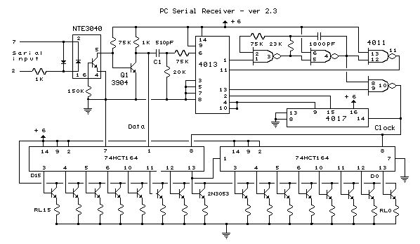
Original scheme edited by Bill
Bowden, http://www.bowdenshobbycircuits.info
This circuit was
designed to control a 32 channel Christmas light show from the PC serial
port. Originally designed with TTL logic, it has been simplified using
CMOS circuits to reduce component count. It is a fairly simple, reliable
circuit that requires only 4 common CMOS chips (for 8 outputs), an
optical isolator, and a few discrete components. The schematic diagram
(SERIAL.GIF) illustrates the circuit with 16 outputs which can be
expanded with additional 8 bit shift registers.
Disclaimer
This circuit requires physical connections be made to the computer's
serial port (COM1 or 2). To the best of my knowledge, it is difficult to
cause damage to yourself or your computer by improper connections to
this port, but there is no guarantee that damage will not result. Use
caution when making any external electrical connections.
Basic RS232 serial
transmission
Serial data is transmitted from the PC as a series of positive and
negative voltages on a single wire which occur at predetermined times
established by the baud rate. Both the transmitter and receiver must be
operating at the same baud rate so that the receiver knows when to
expect the next bit of information. For the PC serial port, baud rate
and bit rate are the same thing, but this is not necessarily true with
modems that can detect more than two states of the line.
In the quiescent state, with no load on the line, the voltage on the
transmit line (pin 2 of the 25 pin connector) will be about -12 relative
to the signal ground (pin 7), which corresponds to a logical
"1". The output impedance of the serial port is about 1K ohm
which yields about 6 milliamps at 6 volts. A typical data transmission
frame consists of a start bit, 8 data bits, and one to three stop bits.
The start bit which is always positive, signals the beginning of the
transmission and is used by the receiver to synchronize the clock so
that the data bits can be sampled at the proper times. After the 9th
time interval passes (start bit plus 8 data bits) a dead time occurs
which allows the receiver time to get ready for the next character. This
dead time is referred to as a stop bit, which is always negative or the
same as the quiescent state. The circuit described here requires two
stop bits of dead time for reliable operation. More sophisticated
circuitry would require only one.
Transmitted character
examples
The letter "A" has a ASCII decimal value of 65. The
"1" and "64" bits are transmitted as a negative
voltage (logical "1"), and the others are transmitted as a
positive voltage (logical "0"). 64 + 1 = 65 = "A"
Circuit operation
The input terminals (pins 1 and 2) of the optical isolator are connected
through a 1K resistor to the transmit and signal ground pins of the PC's
serial port (pins 2 and 7 of the 25 pin connector). A small signal diode
is connected across the isolator input terminals to protect the isolator
from reverse voltage. In the idle state, the isolator input voltage will
be about -0.7 volts and the isolator LED and transistor will be off.
When a start bit is received, about 5 milliamps will flow through the
isolator LED causing the isolator transistor to conduct at about 80
microamps which in turn causes the external switching transistor (Q1) to
turn off. The rising voltage at the collector of Q1 is coupled through a
510 pF capacitor to produce a narrow positive pulse which sets the Q
output of the first RS data latch (1/2 CD4013) and enables the dual NAND
gate clock oscillator.
The clock oscillator runs at a frequency equal to the baud rate (9600
Hz) and must maintain a frequency accuracy of less than 5% over the
temperature range. High stability R and C components are recommended.
The clock output is delayed by one cycle so that the start bit will not
be received as a valid data bit. This is accomplished by the two
remaining NAND gates (1/2 CD4093) and the second RS data latch (1/2
CD4013). One of these gates is used to invert the clock phase so that
the first clock edge seen by the latch (clock pin 11) will be going the
wrong direction and so ignored. The remaining gate, which is enabled by
the second latch, opens on the third clock edge, but also inverts the
clock phase, and so supplies a falling clock edge to the counter and
shift registers which is again the wrong direction, and is ignored. The
fourth clock edge will be rising and active and will occur near the
middle (about 52 microseconds) of the first data bit which will be
shifted into the registers. The remaining 7 bits are shifted into the
registers on each successive rising clock edge. Data is inverted at the
register outputs, a logical "1" will correspond to zero volts,
and a logical "0" will correspond to +6 volts. Transmitting
character (255) will set all outputs low, and transmitting character (0)
will set them all high.
The 4017 decade counter increments one count on each rising clock edge
and resets both data latches on the 8th edge. This in turn stops the
clock and resets the counter, and the circuit remains in a waiting state
until the next start bit arrives. Two stop bits of dead time are
required to allow the voltage at the input of the NAND gate (pin 2) to
reach a logic "1" before the next start bit arrives. Erratic
operation may occur when 2 or more characters are transmitted as a
string and only one stop bit is used.
The circuit may be modified to run at different baud rates by adjusting
the clock frequency. This can be accomplished by temporally connecting
pin 6 of the CD4013 to the positive supply and then selecting R and C
values for the desired frequency. You may need to use a 1% resistor or a
couple 5% resistors in series or parallel to get the value close enough.
Or use a variable resistor in series of about 10% the total value.
At 9600 baud, data output at the shift registers will be unstable for
about a millisecond per word while the incoming data bits are shifted
into the registers and the existing bits are shifted out (into bit
heaven). Higher baud rates will reduce this time proportionally and the
original circuit operates at 57.6K baud to eliminate a slight flickering
of the lights which was noticed at 9600.
The 74HCT164 shift register outputs will sink or source about 4
milliamps at 6 volts which can be increased with medium power
transistors or FETs to drive relay coils, incandescent lights and other
electronic devices. If relays are used, a small signal diode will need
to be added across the relay coil to suppress the inductive voltage.
Power supply
It is recommended that 0.1 uF capacitors be installed near the power
pins of each CMOS device and a well regulated/filtered power supply be
used. For test purposes, a 6 volt battery will work but the clock
frequency will change slightly with power supply voltage variations.
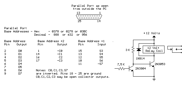
Serial port male D-SUB
connectors as seen from outside the PC.
| |
Output /
Input |
25 pin |
9 pin |
| Transmit
Data |
O |
2 |
3 |
| Receive
Data |
I |
3 |
2 |
| Request To
Send |
O |
4 |
7 |
| Clear To
Send |
I |
5 |
8 |
| Data
Terminal Ready |
O |
20 |
4 |
| Data Set
Ready |
I |
6 |
6 |
| Ring
Indicator |
I |
22 |
9 |
| Data
Carrier Detect |
I |
8 |
1 |
| Signal
ground |
- |
7 |
5 |
| Power line
ground |
- |
1 |
- |
QBasic test program for 8 bit
receiver
CLS
DEFINT A-Z
PRINT "Test sequence in progress, press any key to quit."
OPEN "COM1:9600,n,8,2,CD0,CS0,DS0,OP0,RS,TB2048" FOR OUTPUT AS
#1
Sequence:
FOR Bit = 0 TO 7
PRINT #1, CHR$(255 - (2 ^ Bit)); ' Set
one of 8 outputs high.
SLEEP 1
' Wait 1 sec between characters.
IF INKEY$ <> "" THEN CLOSE :
SYSTEM
NEXT Bit
GOTO Sequence
PC Serial Receiver
(57.6K Baud / TTL & CMOS)
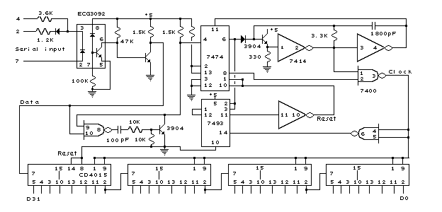
Original scheme edited by Bill
Bowden, http://www.bowdenshobbycircuits.info
Parallel Port Relay
Interface
Here is an example of
controlling a relay from the PC's parallel printer port (LPT1 or LPT2).
The 7.5K resistor is connected to one of the data output lines (D0-D7) and
a common connection is made from the negative side of the power supply to
one of the port ground pins (18-25). Data is inverted by the 3904
transistor so that writing a "0" to the base address will
energize any relays connected to D0-D7 and a "255" will reset
them. You may need to try all three base addresses to determine the
correct address for the port you are using but LPT1 is usually at Hex
0378. The QBasic "OUT" command can be used to send data to the
port. OUT, &H0378,0 sets D0-D7 low and OUT, &H378,255 sets D0-D7
high.
Original scheme edited by Bill
Bowden, http://www.bowdenshobbycircuits.info
Reading Data From The
Parallel Port
The diagram below shows 5
switches connected to the 5 input lines of the parallel port. An external
5 volt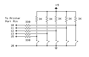 power supply is used to provide high logic levels to the input pins when
the switches are open. Three 1.5 volt batteries in series can be used to
obtain 4.5 volts which is close enough. The 330 ohm resistors in series
with the port connections provide some protection in case a connection is
made to the wrong pin. If you are sure of the connections, the 330 ohm
resistors can be left out and the switches connected directly to the input
pins. The negative side of the power supply should be connected to the
ground point, or any pin from 18 to 25.
power supply is used to provide high logic levels to the input pins when
the switches are open. Three 1.5 volt batteries in series can be used to
obtain 4.5 volts which is close enough. The 330 ohm resistors in series
with the port connections provide some protection in case a connection is
made to the wrong pin. If you are sure of the connections, the 330 ohm
resistors can be left out and the switches connected directly to the input
pins. The negative side of the power supply should be connected to the
ground point, or any pin from 18 to 25.
The following short
QBasic program can be used to read the state of the switches. QBASIC.EXE
can be found in the "OLDMSDOS" directory of the Windows 95/98 CD
Rom. Note that there are three possible printer port address that
correspond to LPT1, LPT2 and LPT3 and LPT1 is usually the one to use which
is at address decimal 889. The program waits for the user to press the
enter key before reading the state of the 5 input lines. The state of the
5 lines is received as a single 8 bit number between 0-255 which is stored
as the value of (V). Each switch input represents a decimal value of
8,16,32,64 and 128 which correspond to pins 15,13,12,10 and 11. The last 3
bits (1,2 and 4) are not used and should return a high level, so the value
received with all switches open should be 1+2+4+8+16+32+64=127. If a
switch is closed and the input is at ground, the value will be 0 except
for pin 11 which is inverted and yields a value of 128 and 0 when high, so
the value received when all switches are closed should be 1+2+4+128=135.
CLS
DEFINT A-Z
Address = 889: REM 889 = port address, other addresses could be 633 or 957
PRINT "Press the enter key to read printer port pins
(15,13,12,10,11)"
PRINT "A (0) reading indicates the pin is at ground level, (1)
indicates"
PRINT "the pin is at a high level or unterminated."
INPUT A$
V = INP(Address)
PRINT V
P11 = 1
IF V > 127 THEN P11 = 0: V = V - 128
IF V > 63 THEN P10 = 1: V = V - 64
IF V > 31 THEN P12 = 1: V = V - 32
IF V > 15 THEN P13 = 1: V = V - 16
IF V > 7 THEN P15 = 1
PRINT
PRINT "Pin 15 ="; P15
PRINT "Pin 13 ="; P13
PRINT "Pin 12 ="; P12
PRINT "Pin 10 ="; P10
PRINT "Pin 11 ="; P11
END
Original scheme edited by Bill
Bowden, http://www.bowdenshobbycircuits.info
Power from RS-232
Here's a circuit I have used (it doesn't guzzle as much current as a 78L05 which is obviously a much simpler
solution):
                                                           +----> DSR
                                             2 X 1N4148    |
                                             +-------------+----< DTR
       +-----------------+-------------+     |      +------+----< RTS
       |                 |C            |    _|_    _|_     |
       |    _____      |/              |    \ /    \ /     +----> CTS
       +---[_____]--+--|   BC550       |    ---    ---     |
       |     10k    |  |\              |     |      |      +----> DCD
       |            |    |E            +-----+------+-----------> V++
    +__|__          |    +----+---------------------+-----------> VDD
     _____    +-----+         |    _____            |             +5V
  220u |      |     |         +---[_____]---+       |
       |      |    C|               22k     |    +__|__
       |    __|__    \|  BC547              |     _____
      ///   _____     |---------------------+   47u |
         100n |      /|                     |       |
              |    E|              _____    |       |
              |    _|_        +---[_____]---+      ///
             ///   \ /^       |     18k
                   ---        |
       LO-I RED LED |         |
                    |         |
                   ///       ///
Strapping DTR/DSR and CTS/RTS/DCD is just to implement a "null-modem" connection, the power comes
from DTR and RTS.  On a typical PC about 5mA can be drawn from the regulator.
Ham radio Data Center - free schematics | 73s.eu - Free Ham Radio Social Network | Free HAM Directory | About me | Acronyms | CW | Data Sheets | Docs | Download | E-mail | HOME | Ham projects | Hobby circuits | Photo galery | PIC | QTH photos |
Sign in my guestbook | View my guestbook ]
© 2001 - YO5OFH, Csaba Gajdos
|