
| ADVANCED LESSON 35 | |
| LEARNING OBJECTIVES and NOTES | |
| Oscillators | |
|
4b.1 Understand the function of the components in typical VFO and crystal oscillators. The drawing opposite shows a typical VFO oscillator. The common emitter amplifier, formed by the transistor, amplifies the current imposed on the base bias voltage. R1 and R2 control the bias. The choke allows the DC current to flow to and through the transistor from C to E. At AC the choke forms a high impedance, this prevent AC entering the choke. An AC voltage is created at the collector, some of which is fed back to the resonant circuit L1 C1/C2 to maintain oscillation. An output is taken via C2 to the next stage. The actual frequency of oscillation is maintained by the resonant circuit L1 / C1/C2. |
 |
| Frequency synthesis | 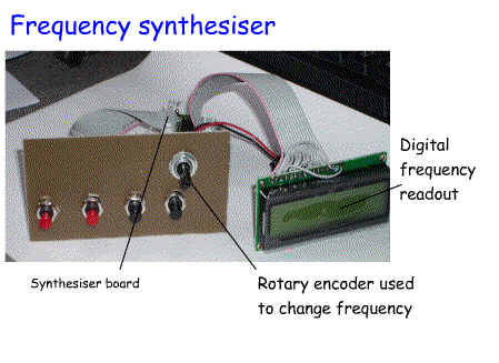 |
|
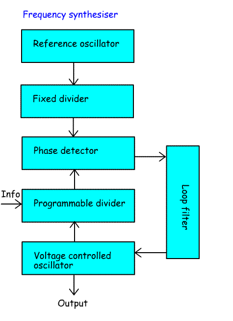
4c.1 Recall the block diagram of a frequency synthesiser and the
functions of the stages (i.e.oscillator, fixed divider, phase detector,
LPF, voltage controlled oscillator and programmable divider). In many radios the frequency synthesiser has replaced the VFO, mixers etc. used to generate a range of frequencies. The purpose of a frequency synthesiser is to produce a sine wave with the stability of a crystal oscillator combined with the flexibility of a VFO. These are the functions of each stage (see drawing opposite) Reference oscillator This is a stable crystal controlled oscillator (e.g. 1MHz). It is temperature stable and has low noise Fixed divider This divides the oscillator output by a fixed amount (say 1000 to give a frequency of 1MHz / 1000 = 1kHz). The output is the step size of the synthesiser.  Where Fstep = output step size of the synthesiser f = frequency of the crystal A=value of fixed divider The Phase Detector This has two inputs and one output. One input comes from the fixed divider and the other from the programmable divider. The output is a correction voltage used to control a varicap diode which in turn controls the frequency of a voltage controlled oscillator. If the phase (frequency) of the two inputs is the same the voltage remains constant and the VCO does not change frequency. If the phase (frequency) of the two inputs is different the voltage output adjusts the VCO and changes the frequency. This process continues until the two signals are in phase or at the same frequency. The system known as a Phase Locked Loop (PLL) is said to be locked. The Programmable Divider To vary the frequency the frequency divider is changed by either BCD switches, PICS or even toggle switches. The input to the programmable divider comes from the VCO. The output is one of the inputs to the phase detector. The Voltage Controlled Oscillator This is an oscillator controlled by the voltage from the phase detector. It has to be thermally stable, mechanically stable and have low noise. The Loop Filter This is a low pass filter with a cut off of between 100Hz and 10kHz. It filters out unwanted signals from the phase detector. The formula for calculating an output frequency is:  Where Fout = frequency output from synthesiser fcrystal = frequency of reference crystal N = number from the programmable divider A = number from the fixed divider The step size for Example 2 would be 12.5kHz The phase (frequency) detector compares the 12.5kHz fixed frequency with the output from the programmable divider. If the two are in phase the output frequency is correct and the voltage to the voltage controlled oscillator (VCO) remains constant. If there is a phase differences a voltage is output to the VCO to shift the VCO frequency. This is again divided down by the programmable divider and compared to the 12.5kHz reference in the phase detector. This continues until there is no phase difference because both inputs are 12.5kHz. The system is said to be locked. There is usually an additional bit of circuitry preventing a PLL controlled transmitter transmitting when out of lock! This is called an out of lock inhibitor. |
 Example 1
Example 2
 |
|
Recall how sine waves may be produced by direct digital synthesis and
the block diagram of a simple synthesiser. Recall that increasing the
number of bits in the synthesiser will increase the purity of the
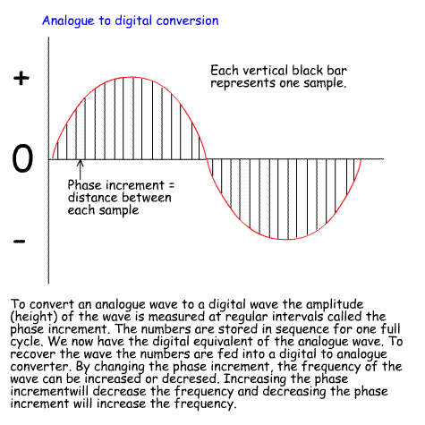
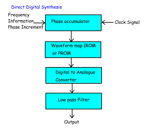
signal. Analogue to digital conversion The direct digital synthesiser produces a sine wave from a set of numbers. The drawing opposite shows how the amplitude of a sine wave can be measured at regular intervals (the black vertical lines). The more readings are taken the purer the wave. This will also increase the number of bits stored in the synthesiser. The drawing also shows that if the numbers are stored in order they can be fed back into a digital to analogue converter to recreate the sine wave. In addition by changing the phase increment the frequency can be changed. A shorter phase increment will shorten the wave and so increase the frequency and vice versa. The diagram shows the basics of a direct digital synthesiser. The phase accumulator stores a binary number from information about the clock signal, frequency and phase increment. This passed to the waveform map in ROM or PROM where the numbers representing the regular samples are fed to the digital analogue converter. Which recreates the sine wave. A low pass filter removes unwanted signals. The synthesised wave is produced at the output. In modern transceivers the frequency is controlled by a combination of DDS and PLL type technology. |
  |