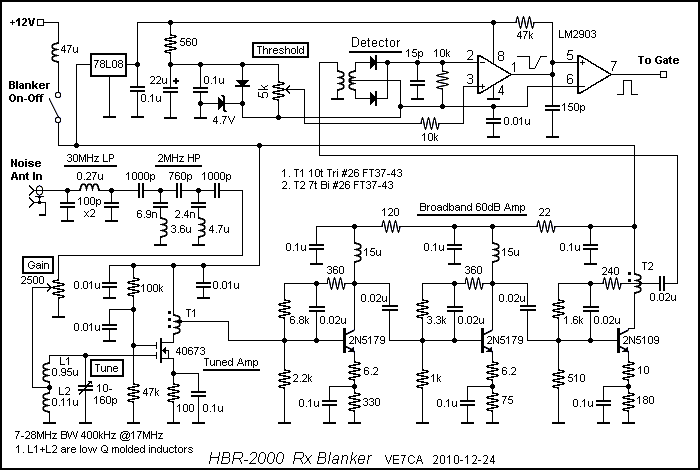
|
HBR-2000 HF 160 to 6 meter High Performance All-Mode
Transceiver
New Page in Progress
Latest Updates:
2010 Dec 01: Added
Noise Blanker information here. Blanker
2009 Jan 19: Added photos of 100 Watt Amplifier stage. 100 Watt Amp.
2008 Jan 12: Added note regarding compensationg VFO
Drift:VFO and Frequency Control
2006 Dec 20: Revised Receiver Measurements. New Measurements
2006 Dec 18: New Receiver Front End here. New Front End
2006 Dec 04: New VFO details. VFO and Frequency Control
2006 Apr 17: New section added for Front Panel Design Front
Panel Layout
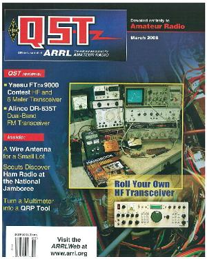
2006 Mar 14: QST publishes article on the HBR-2000
This page provides a brief description of the receiver portion of a HF (160 to
6 meters) High Performance Transceiver that I built. I named it the HBR-2000.
HBR is short for homebrew and 2000 is the year that I first heard a signal
from the receiver speaker. This section, hopefully, will be an incentive to
those who read it to build their own amateur radio equipment. I am not an
electrical engineer, just a true amateur radio operator who likes to learn
and build radio equipment with my hands.
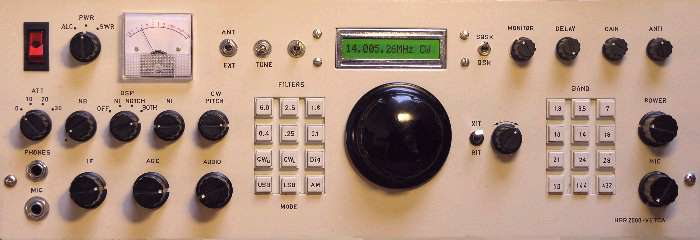
Front Panel View
For many years I dreamed of building a high performance multi-mode HF
transceiver. However, priorities such as family and work left little time to
take on a major project like the HBR-2000. In my early years as a ham radio
operator, I built several Heathkit transmitters and
transceivers and later as I gained experience I began homebrewing
solid state direct conversion receivers and QRP single band transmitters. In
1998, I decided that it was time to stop dreaming of building a high
performance transceiver. The HBR-2000 is my dream come true.
I have attempted to miniaturize the HBR-2000. I have found when I had the
opportunity to use some of the current high end transceivers that the knobs
are very small and closely spaced. When adjusting one knob, it is easy to
touch and move another knob and not know it. Also many functions employ
concentric knobs and the labels are very small and not easy to read in low
light. Small is OK for portable rigs but for a home station transceiver one
should be able to adjust one knob and not have to worry about touching
another. With large knobs and large labelling, I am able to operate my
transceiver without the need for my reading glasses.
Quick Links
1. Receiver Measurements
2. Design Process
3. IF-Detector Module
4. Audio Module
5. VFO and Frequency Control
6. RF Filters
7. Front End, Mixer, Post Mixer Amp and Noise Blanker
Gate
8. Front Panel Layout
9. Transmitter 100 Watt Amp.
10. Test Equipment
11. Keeping Records
1. Receiver Measurements
I have only measured the 2 tone Dynamic Range (DR) and 3rd Order IMD receiver
measurements on 20 meters. The MDS measurements on all bands are within + or
- 0.5 dB of -130 dBm with the Pre Amp-Amp. turned OFF. All measurements
were made with an IF filter BW of 400 Hz. Test oscillators are two xtal osc's, low pass filtered
and designed for 50 ohm output impedance. MDS measurements made with a
HP8640B signal generator and a true reading RMS volt meter across the speaker
output.
The following measurements were made on December 20, 2006 after installing a
"New Front End Circuit" following ARRL procedures as outlined in
the ARRL Lab Test Procedures Manual. If you are a ARRL member, you can find a
copy of this document at http://www.arrl.org/test-procedures-manual.
Test
Measurements (New Front End, including RF pre-amp) December 20, 2006
PRE-AMP OFF PRE-AMP ON MDS (Sensitivity) -130 dBm -139 dBm Image rejection all bands >135 dB |
MEASUREMENTS WITH PRE-AMP OFF. Spacing 20 kHz 5 kHz 2 kHz BDR (2 tone Blocking Dynamic Range) >134.0 dB >134.0 dB 126.0 dB 3rd Order IMD (Intermodulation Dynamic Range) 106.3 dB 106.3 dB 103.2 dB Third Order Intercept (IP3) 28.5 dBm 28.5 dBm 23.5 dBm MEASUREMENTS WITH PRE-AMP ON. Spacing 20kHz 5 kHz 2 kHz BDR (2 tone Blocking Dynamic Range) >130.0 db >130.0 db 124.0 db 3rd Order IMD (Intermodulation Dynamic Range) 103.0 dB 103.0 db 101.0 db Third Order Intercept (IP3) 17.5 dBm 17.5 dBm 13.7 dBm |
Receive to Transmit Time 8 ms (incl. 4 ms click filter) (CW, Full QSK) Transmit to Receive Time 8 ms (30WPM = 20 msec dot) |
Third Order Intercept (IIP3) measurements were determined using ARRL's
preferred method using a S5 (S meter reading of 5) reference signal level
instead of MDS with the AGC turned on. IIP3 is calculated as (3*(S5 IMD
Level)-(S5 Reference))/2. ARRL Lab Supervisor describes ARRL's reasons for
using a S5 reference level when determining IIP3 in QEX Jul/Aug 2002 p. 50.
As noted in the article, IIP3 taken at different S meter reference points
typically produce IIP3 numbers that vary from the S5 reference level. As an
example, at an S9 reference level, the HBR-2000 IIP3 at 5 KHz spacing is
quite a bit higher at +33 dBm. However, it is very
likely that when close osc. spacing such as 5 and 2
KHz is used, the AGC is responding to the very strong off-channel signals.
It is estimated that the above measurements are accurate within a range of +
or - 1.0 db.
W8JI, a 160 meter
enthusiast, has an interesting Web page where he presents his views on
receiver specifications at http://www.w8ji.com/receiver_tests.htm.
From his experience, when comparing receiver performance, a high 3rd Order
IMD is the most important factor to consider. The majority of the commercial
amateur radio transceivers have wide roofing filters. This often results in
severe IMD in a contest environment where you are attempting to copy a weak
station amongst several very strong signals spaced less than 1 KHz apart.
That is why W8JI has been including 2 KHz test oscillator spacing when he
tests a receiver.
The HBR-2000 with the "New Front End Circuit" has an IP3 IMDR of
102 dB at 2 KHz osc. spacing which is 7 dB higher
then the Ten Tec Orion II, 24 db higher than the Yaesu FT-9000 and Icom IC-7000,
42 dB higher than the FT100MP-Mark V and at 5 kHz spacing, 27 dB higher than
ICOM 756PRO-III.
Before the article about the HBR-2000 was published in the March 2006 issue
of QST I shipped the HBR-2000 to ARRL Headquarters and it was tested in
ARRL's lab. where the receiver measurements were confirmed as being correct.
This was before the "New Front End Circuit" was installed. The old
front end measurements are not significantly different than the "New
Front End Circuit" other than the "New Front End Circuit" with
the RF Pre-Amp. switched on is approx. 10 db more
sensitive.
Two discussion papers addressing receiver measurements you may wish to read
are:
"THE THIRD ORDER INTERCEPT POINT (IP3)" by SM5BSZ's:
and,
NC0B, Ron Sherwood's paper titled,
"A DISCUSSION OF MEASUREMENT ACCURACY AND SAMPLE VARIATION"
Obtaining
accurate IMD measurements is not a trivial matter and should be approached
with a sound technical understanding of the possibilities for error.
HBR2-2000 transmitter specifications are: CW/SSB/Digital, 160 to 6 meters, 9
watts output and full QSK on CW. See the QEX article listed at the bottom of
this page for information about the QSK system. A 100 watt amplifier is
housed in a separate enclosure along with the power supply. The final
amplifier incorporates a single MRF151 power MOSFET running on 48 volts. It
is followed by separate diplexers and elliptical LP filters for each band.
All harmonics and image products are 58 db or more
below the carrier level.
2. Design Process
The design process began by deciding on features and specifications that
would suite my particular operating style. With other hams in close
proximity, the receiver had to have a very strong front end. As well, I often
operate in various contests so good selectivity is important. Smooth QSK
operation was also considered an important feature. Though I operate mostly
CW I still wanted the capability of operating SSB. In addition, being able to
listen to AM is a feature that I would appreciate.
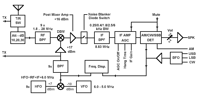
I began by drawing a block diagram of the receiver portion. I broke it into
several modules so that I could build one section at a time and then test it
before proceeding with the next stage. Each section, when completed, was
enclosed in a box made of PC board copper clad material. The circuits are
designed for an impedance of 50 ohms going into and out of each box. BNC
connectors are used for all RF connections between the individual boxes. DC
and control lines enter the individual boxes via feed thru capacitors.
Block
Diagram of the receiver portion of the HBR-2000.
Since I am not an electrical engineer I am aware of my limitations as far as
designing circuits. Why re-invent the wheel when someone else has already
gone though the trouble? Therefore, where suitable, I used circuits from
various designs that have been published in amateur radio periodicals such as
QST, QEX, The ARRL Handbook and books such as, "Solid-State Design for
the Radio Amateur" by W1FB and W7ZOI and "Introduction to Radio
Frequency Design" by W7ZOI.
You may find further information regarding these publications at the
following Web site:
· http://www.arrl.org/shop
The latest ARRL technical publication "Experimental Methods in RF
Design" by Wes Hayward, W7ZOI, Rick Campbell, KK7B, and Bob Larkin,
W7PUA is is highly recommended for anyone
contemplating the thought of building their own radio equipment. This work is
successor to "Solid-State Design for the Radio Amateur" which was
first published in 1977. EMIRFD, is 512 pages of fascinating reading and
includes a CD-ROM with design software, listings for DSP firmware, and
supplementary articles. © 2003, published by American Radio Relay League
(ARRL). (ISBN: 0-87259-879-9) Revised first edition. © 2003-2009 #9239 --
$49.95
There is a wealth of information in this publication applicable to
homebrewers!
When I found a design for a section that I liked and a PC board was available
I purchased it, otherwise I used what is referred to as "ugly
construction". Ugly construction is the process of using copper clad PC
board material for a base to build electronic circuits on.
Once I had chosen the circuits for each section I asked a
friend to look it over and make suggestions and point out things that I
hadn't considered. It is a very good idea to be friends with an Elmer, i.e.
someone that knows more than you and is experienced in not only designing but
actually building electronics circuits.
5. Frequency Control
Since low oscillator phase noise is one of the pre-requisites to obtaining a
high overall receiver dynamic range, I used a low phase noise analog VFO and
mix the output of the VFO to the required injection frequency with separate
crystal oscillators which are have a very low phase noise, for each of the 10
lowest amateur radio bands from 160 meters to 6 meters. The VFO tuning range
is 1 MHz, (later changes to two 500Khz conseceuive ranges) I can thus tune from the low end of 20 meters up to WWV at
15MHz. As well, a 1 MHz tuning range allows me to cover the lowest 1 MHz of
ten meters without having to add another crystal oscillator.
An analog VFO is considered by many as old technology, however it is much
easier to make a clean, low phase noise analog VFO than a digital VFO.
Technology is improving daily and no doubt it won't be long before you will
be able to purchase a single IC that will do the job of an analog VFO with
similar spec's but until then, the analog VFO is still king!
The VFO main capacitor came from a WWII aircraft transmitter called the
ARC-5. It is beautifully made. The capacitor is silver plated with ball
bearings on both ends of the main rotor. The reduction gear comprises two
gears, one fixed and the other floating with a spring pulling them together
as they mess with a worm gear preventing what is called "back-lash"
or a lag when changing direction. Before putting the capacitor into service I
removed the reduction gears. I then soaked all the parts in solvent for
several days to loosen all the accumulated dirt and grime. Remember these
capacitors are over 70 years old. I then blew out the bearings with a high
pressure hose, re-assembled it and then oiled the bearings and the two
reduction gears before re-assembling. The VFO is silky smooth now. The
attached picture shows the main VFO capacitor with the new (November 2006)
dual range VFO circuit board attached to the back.

Originally I built the VFO to cover a one MHz range (5 to 6 MHz), however I
found that 22 KHz per one turn of the VFO knob was too fast when using the
narrow 170 Hz audio filter. The revised VFO has two consecutive 500kHz ranges
selected from the front panel with a toggle switch that operates a latching
relay located next to the VFO inductor. It is important to use a latching
relay as a regular relay coil when energized will heat up and since it is located
next to the VFO main inductor, the VFO will drift with the increase in relay
coil temperature. The dual range VFO now tunes approximately 12 KHz per turn
of the VFO knob, perfect!
One of the factors that effects phase noise of an oscillator is the unloaded
Q of the VFO inductor. The higher the Q, the lower the phase noise of the
oscillator. I was able to achieve a Q of 370 by epoxying two T-68-6 toroid
cores together and using #18 guage wire for the
inductor winding. The VFO circuit is based on an article by J Makhinson, N6NWP. Communications Quarterly, Spring 1999
page 9-17. Makhinson provides extensive details in
the article about designing very low phase noise VFO oscillators. High main
inductor voltage, loose coupling to the inductor and a low noise devise such
at the J310 all contribute to the low phase noise of this oscillator circuit.
The VFO circuit has it's own power supply which is never turned off and it is
also compensated for freq. drift with a N150 neg. temp. capacitor. Drift is
so insignificant that I can use the digital modes with out any problem. The
following picture shows the VFO ready to put back into the enclosure.

The
circuit for the new dual range VFO
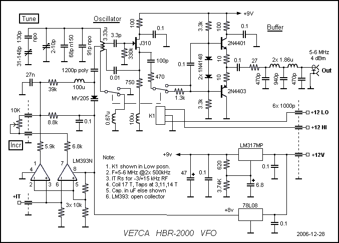
Not shown on the VFO diagram is a 14 db attenuator
to reduce the output to -10 dBm, the required input
into the HFO mixer. The crystal oscillators are biased for +7 dBm. The VFO is filtered with a 2 section LP filter to
attenuate harmonics.
When building the RIT/XIT circuit you may want a different tuning range. My
RIT/XIT tunes 3 kHz below and 15 kHz above the centre
freq. If you go to the DESIGN page and click on Tools, #6 has a tool that
allows you to determine the correct bias resistors for different incremental
tuning ranges.
Overall phase noise is not a limiting factor in regards to the two tone
dynamic range of this receiver because of the inherent low phase noise of
crystal oscillators and the low phase noise VFO circuit I used.
Frequency Drift
Frequency drift can be an issue with analog VFO's so I decided to try to
improve the frequency drift while changing the VFO to encorporate
two ranges. Not that the drift was bad, +or- 20Hz once the VFO warmed up, but
I was sure it could be improved. With no excuse not to address the drift
situation I built a tempature sensor with a LM335
and intalled it in an old Coleman picnic cooler as
a heat chamber. It includes a shelf and below the shelf is a bulb with an
on/off switch, (I used a 40 Watt bulb for a slower temp. rise) and a fan. Wes
describes the use of a temperature chamber (or warming oven) on page 4.5-4.6
and also 7.42 in EMRFD. A more detailed description is in the original QST
article, Dec 1993 page 37.
After several runs with the VFO in the chamber and running the formula's in
EMRFD I determined that if I replaced an existing 50pF N150 with a 68pF N150
cap I should be able to nail the drift right on. I couldn't find one. No one
stocks polystyrene caps around here either. I tried combining two caps in
series, a 100pf N150 and a 220pF NPO and a couple other combinations but to
no avail. I then remembered that I was given a box of parts when my friend
VE7YQ passed away several years ago. I searched the attic and found the box
and sorting though the stuff I found a box of ceramic capacitors. In it was a
68pF N150 in perfect condition, never used before and I suppose it was at
least 50 years old. I popped it in the VFO, let it stabilize over night and
the next morning I measured a +3.2 ppmC. Wow, I
couldn't believe it so I ran another test later that same day the result was
similar. I have since put the VFO back into the transciever.
Monitoring the VFO ouput using my HP8640 counter,
the VFO is stable to +or- 5Hz over a half hour period. Not bad for an analog
VFO using a 70+ year old WWII tuning capacitor and other assorted old parts.
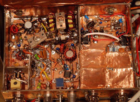
Inside
view of the HBR-2000.
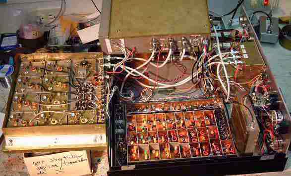
The crystal. osc. boards and mixer are to the left,
the BPF's in the middle and the transmitter box is folded towards the back
lying on top of the receiver Mixer, IF and Audio boxes. The frequency counter
is to the right with the VFO underneath. Below the frequency counter standing
upright is a box housing the noise blanker TRF receiver. The transceiver is
built so that each section can be either folded out and away from the main
transceiver chassis or easily removed for testing and maintenance purposes.
The VFO and Crystal oscillators are fed into a double balanced diode mixer
and then filtered by 10 separate relay switched 2 section Series C BPF's
(bandpass filters). Some may question the wisdom of using only a 2 section
filters at this stage, however the receiver input BPF's (which are also
shared with the transmitter) are 3 section filters and provide adequate stop
band attenuation. After filtering, further amplification increases the LO
power output where it is split into three separate outputs, +17 dBm for the receiver mixer, -5 dBm
to the transmitter board (later to be amplified to +7 dBm
for the transmitter mixer) and a low level output for the frequency counter.
When I first built the LO system I did not pay attention to setting the VFO
output level and for reasons I can't remember, the VFO output was 0 dBm. After connecting the LO to the receiver mixer I
found a number of spurs that shouldn't have been there. Wes, W7ZOI came to my
rescue explaining the importance of not driving the RF port of a balanced
mixer with more than -10 dBm. After decreasing the
VFO output to -10 dBm the spurs disappeared. The
VFO is built into a box made of PC board material. The 10 crystals
oscillators and LO mixer are built into the top half of a box made of PC
material. The bottom half of the box contains the 10 BPF's and an amplifier
to boost the LO output power to the desired level.
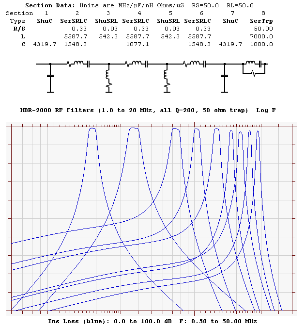
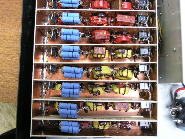
6. RF Filters
Filters, play an important role in the development
of high performance receivers and transmitters. The HBR-2000 contains over 30
separate filters. One test instrument that I found invaluable is the L/C
Meter kit produced by Almost All Electronics Inc. This test instrument allows
the experimenter to quickly determine inductor and capacitor values. When
winding toroid coils, I calculated the number turns required for the desired
inductance value and then after winding the coil I measured the value with
the L/C meter. If required I then squeezed or expanded the turns until I
reached the correct value. This process saved many hours of tuning filters
after they were built. The L/C meter is also helpful in determining the value
of poorly marked capacitors which seems to be all too common these days. You
may find information regarding the L/C meter at:
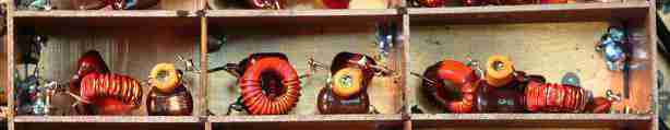
Picture below shows one of the ten BPF's shared between the receiver and
transmitter. The filters are shielded from each other in addition to having
shields between each sub-section of each filter.
Typical RF BPF.
All the filter component values used in the HBR-2000 were derived using a
program that my friend developed. See the Design Page on the main menu bar of
this Web site for further details. I have found this program indispensable.
It contains many other features besides filter design such as, a VFO
component calculator, an impedance matching circuit calculator, mixer
spurious image calculator, an active IC filters design and a Calculator page
that has a number of other useful features such as, the reactance of
capacitors and inductors, resistive attenuator values, an air coil calculator
and receiver noise analysis program. It is easy to use and provides very good
quality graphs showing attenuation and input return loss.
Below is a copy of the graph produced by the RF Design Program for the 14 to
15 MHz BPF filter that precedes the receiver mixer in the HBR-2000 (filter
output [to mixer] is actually on the left to show match to mixer!). The 14.5
MHz series trap matcher (diplexer) terminates the mixer RF port in 50 ohms
over a broad frequency range improving the 3rd order input intercept of the
receiver mixer.
Below is the design for my
14 MHz filter with input trap match (diplexer).
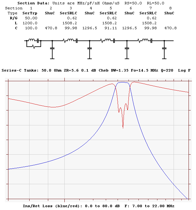
Notice that the insertion loss (blue line) of the filter increases more
rapidly above the design frequency than below. This provides greater
attenuation at VHF/UHF frequencies where local high power TV and FM stations
are located. This diminishes the possibility of these out of band signals
reaching the mixer and combining with VFO and HFO harmonics and mixer
products that can produce unwanted spurious signals in the receiver.
14 MHz. RF BPF Response.
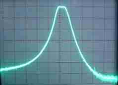 This is a picture of the
spectrum analyzer screen showing the characteristics of the 14 MHz BPF
filter. The left side of the screen indicates an attenuation at 7 MHz (40
meters) of -58 db and the right side is 21 MHz (15
meters) with an attenuation of > -65 dB.
Horizontal divisions are 10 db. This is a picture of the
spectrum analyzer screen showing the characteristics of the 14 MHz BPF
filter. The left side of the screen indicates an attenuation at 7 MHz (40
meters) of -58 db and the right side is 21 MHz (15
meters) with an attenuation of > -65 dB.
Horizontal divisions are 10 db.
For 160 and 80 meters I used Series L BPF's. The insertion loss of Series L
BPF's increases more rapidly below the design frequency than above. This
helps attenuate local strong AM broadcast stations. At my QTH there is an AM
station at 980 kHz which is very strong. The filter I designed has an
attenuation at 980 kHz of over 70 db. With a 160 half wave loop tuned for
minimum SWR at 1.85 kHz, I inserted the 160 meter BPF between the antenna and
my TS940s and tuned it to 980 kHz, I measured attenuation at 68 dB. I have no birdies on 160 or 80 meters caused by AM
broadcast stations with the filters I designed for the HBR-2000.
160 meter filter design
with output (mixer side) trap diplexer and insertion loss curves for all
bands.
All the RF input filters are built inside a box made of PC board material.
The box is subdivided into 10 sections, one for each filter with additional
shields between each sub-filter section. I have measured stop band
attenuation in excess of 96 db with the cover on
the filter box. All of the filters in the HBR-2000 are switched with relays.
Many commercial amateur radio transceivers use diodes to switch between
filters. Diodes switches can introduce IMD in the presence of other very
strong RF signals. European hams in particular are aware of this problem as
40 meters is also occupied by very strong AM shortwave stations.
Relay Troubles: November 15, 2003
There is a problem associated with using relays to switch very low RF levels.
I noticed over the period of several years that some of the relays used to
switch the input BPF's did not close completely the moment a particular band was
selected. For example, when I changed bands, the receiver antenna noise
sometimes was lower than usual for 10 to 60 seconds and then all of a sudden
the antenna noise would rise to the expected level. This was confirmed by
looking at the 15 meter BPF with the spectrum analyzer and tracking osc (this band gave me the most trouble). As pointed out
by Peter, G3RZP in Letters to the Editor, page 58 in QEX Sept/Oct this
problem is associated with oxidation of the relay contacts. This solution is
to run a constant DC current through the relay contacts when they are closed.
I recently added resistor dividers to pass approx 7
mA DC through the input RF filter relay contacts when switched on. Initially
this did not solve the problem so I increased the current to 100 ma DC and
switched the relays on and off many times (50 to 100 times worked for me) to
clean the contacts. After the contacts were clean, I reverted back to the
lower current circuit. I no longer have problems with the relays.
7. Front End, Mixer, Post
Mixer Amp and Noise Blanker Gate
The mixer circuit I employed at first was a double balanced diode circuit
with +7 dBm LO power. Wanting to increase the
dynamic range of the receiver I changed the mixer to a Mini Circuits TUF-1H
which requires a LO power of +17 dBm. The change in
mixer and increase in LO power did not increase the IP3 as expected. A double
balanced diode mixer with an LO of +17 dBm should
be able to produce an IP3 of approximately +23 to +25 dBm.
I was only achieving +14 dBm. John Stevenson,
KD6OZH, wrote an excellent article titled "Reducing IMD in High-Level
Mixers" in May 2001 QEX, page 45. He examined how IMD was effected by
the impedance match (SWR) looking into all the ports of high level double
balanced diode mixers. He found that having a good match (low return loss)
into the RF port was as important as the IF port. In order to achieve a low
return loss at the RF port he employed a diplexer between the front end BPF
and the mixer. When I inserted a diplexer between my 14 MHz BPF and the mixer
the IP3 increased from 14 dBm to 25.5 dBm. I have since added diplexers to all the receiver
input band-pass filters in the HBR-2000. The IMD, two tone dynamic range,
(tones spaced 20 kHz apart), increased from 97db to 106 db
with the new mixer and at 2KHz tone spacing it is now 103 dB, well worth the
effort.
Since I recently added 6 meters capability to the HBR-2000, I decided that I
wanted more sensitivity on that band in particular so I decided to build a
"New Front End Circuit". The "New Front End Circuit"
incorporates three relay selected 10 db attenuator
pads, a relay selected RF PRE-AMP, the mixer, and two post mixer amplifiers
with a Delay BPF inserted between the amplifiers followed by the noise
blanker gate.
After making measurements I found that a diplexer was not needed with this
design. The high input and output return loss of the two post mixer
amplifiers and the 10 db loss of the BPF provides
sufficient isolation between the mixer output and the input to the xtal filters so typical large variations in xtal filter input impedances are not reflected back to
the mixer output port.
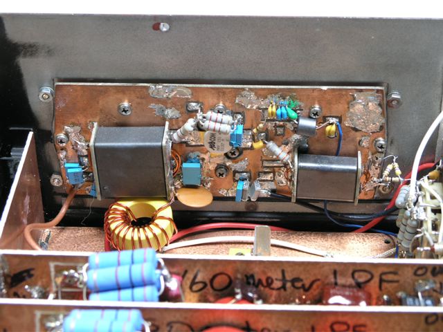
The following picture shows the "New Front End Cirucit".
Note the copper shield over the 10 dB step attenuators and the +17 dBm LO input to the mixer. +17 dBm
is a lot of power near the receiver front-end that has sensitivity of -138 dBm. It is a good idea to keep this level of RF power
from getting into places it shouldn't be! Good shielding accomplishes this.
The second set of diodes in the blanker gate is also shielded which improves
the isolation when the diodes are biased OFF. The RF PRE-AMP is located in
the top right hand corner subsection, the two Post Mixer Amplifiers with the
Delay BPF are shown in the middle section.
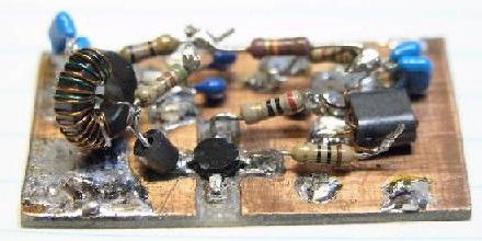
The RF PRE-AMPS were built on separate double sided PC boards. I used a Dremel tool to make pads for the component connections.
After testing they were inserted in the Front End box. The RF PRE-AMP
transistor is a low noise UHF transistor (MRF581A) which has to be treated
with care to prevent UHF osc. The 5 pf cap. at the
junction of the base and 10 ohm resistor kill UHF osc.
in the amplifier. Short component leads are very important with this
amplifier.
The New Front End performed better than I had expected. The Input Third Order
Intercept and Two Tone Dynamic Range increased over the old front end design
and the sensitivity when the RF PRE-AMP is selected is -139 dBm +/- 1dB. The increased sensitivity has proven
especially helpful on 6 meters. Even on 15 to 10 meters, when my yagi is pointed away from the city where the noise floor
is very low, the increased sensitivity does make the difference between being
able to copy a very weak station or not.
RF,
Mixer, Gate Circuit.
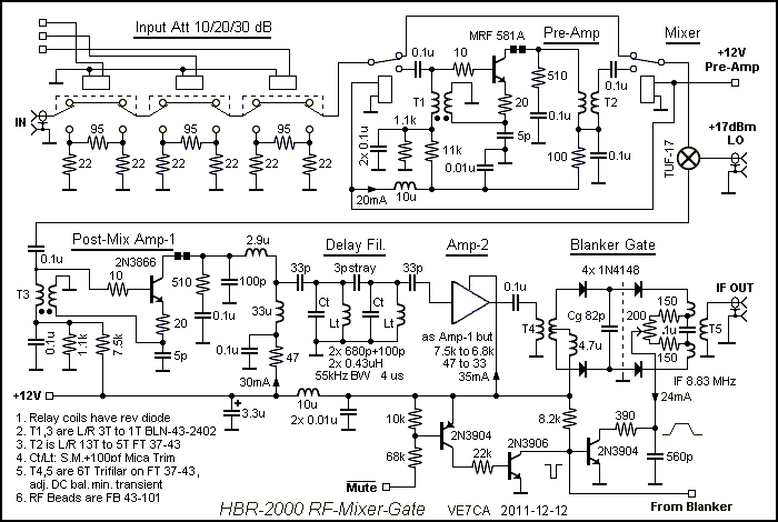
It is important to use one DPDT relay for each 10 db
attenuator, making all leads as short as possible to preserve the 50 ohm
impedance and reduce stray inductance. I chose a modified Low Noise Norton,
single ended, unbalanced circuit for all the amplifiers in the New Front End
for it's excellent input to output reverse isolation and it's simplicity. The
measured return loss at the input and output exceeded 20 db,
and that is with the opposite end either terminated in 50 ohms, shorted to
ground, or open! The RF PRE-AMP is biased for 20 mA and achieves an Output
3rd order intercept (OIP3) of +33 dBm and the gain
is flat to within +/- 1 db from 1.8 MHz to 50 MHz
with the UHF MRF581A transistor. Using a 2N3866, (I didn't have any more
MRF581A's) the first post mixer amplifier is biased for 30 mA with an OIP3 of
+38 dBm and the 2nd post mixer amplifier is biased
at 35 mA and has an OIP3 of +40.7 dBm. A number of
other transistors are suitable for the post mixer amplifier circuit such as
the 2N5109, 2N3553, 2N5943, BFR-94 and for a SM transistor try the NE46134.
If you want a low noise transistor and are unable to obtain a MRF581A try to
obtain a 2N3866 as this transistor has a low base spreading resistance. Low
base spreading resistance helps to achieve a low noise figure with high
collector current.
I used to use a relay to disable the Mixer LO drive on transmit to improve my
QSK system such that I can hear between characters when I am sending CW at 30
WPM but changed to just adding a Mute input to the blanker to avoid
the relay and get a slight improvement. The Mute line is timed so that
it is active just before to just after TX and prevents TX leakage causing the
crystal filters to ring. Check this link for a copy of an article published
in the March/April issue of QEX 2006; "Perfecting A QSK System" by
VE7CA. QEX Mar-06, Perf. QSK (Copyright
ARRL. All rights reserved, used with permission of the ARRL.)
The Delay BPF, located between the two post mixer amplifiers, delays IF
incoming noise pulses about 4 us. This allows time for the noise blanker
diodes to be biased off before noise pulses arrive at the diode gate. Great
care must be used to build that Delay BPF. I used the largest core that would
fit in the allowable space (T-68-6) and #18 guage
wire for the Delay BPF in order to achieve the highest Q possible. The photo
(below-left) shows a tubular top coupling capacitor, however it was later
removed as there was sufficient stray coupling between the two coils (the
theoretical value is only 3 pF!). I adjusted the spacing between the coils to
achieve optimum coupling with measured BW of 58 KHz.
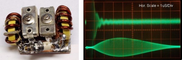
The photo (above-right) clearly shows how filters stretch
signals as they pass though (group delay is the average delay time of the
energy, the time-domain representation changes and it is not just delayed). A
typical powerline RFI noise pulse has a very short rise time,
<10 nS! The top trace in the picture below is the ouput of the Noise Receiver showing a noise pulse delayed by the Noise Receiver single tuned 440 KHZ wide input stage. The bottom trace is the noise pulse after passing through the HBR-2000 receiver front end filters and the Delay BPF.>
Cg, the 82pF cap. between the legs of the balanced diode gate cancels the
inductive reactance of the gate. The value was determined by inserting a
variable capacitor and tuning it for maximum attenuation of the gate switch,
then removing the variable cap and measuring it's value with a capacitor
meter. I then soldered in a fixed value cap. to replace the variable cap. To
achieve best performance, wire the Blanker Gate's T4 and T5 with very short
leads and adjust the 200 ohm balance pot for minimum switching transient at
the Gate output.
The use of my home made RF Pulse Noise Generator was essential in the
refinement of the noise blanker. You can find a circuit diagram of the RF
Pulse Noise Generator on my Testing page here.
Note thet I used 1N4148's for the gate diodes. I
made comparative measurments between 1N4148's and
HP 5082-2810 Hot Carrier Pin diodes. The differences between the two diode
types in regards to loss, attentuation, switching
time and Intermodualtion Distortion were so nominal
that I feel it is not necssary to use the more
expensive HP Pin diodes for this application. The measured loss through the
gate is only 0.1 dB and when baised off, the
attenuation is 78 dB. This equates to 13 S units (6
dB per S unit) of noise pulse attenuation!
If you are using an IF of 9 MHz, monolithic filters with a BW of 20 KHz are
available as a substitute, however do not use a BW of less than 20 KHz as the
narrower the BW, the greater the noise pulses widen and hense
the longer the blanking diodes have to be biased off producing a wider hole
in the RF signal path. A 20 KHz BW delay filter will increase the group delay
of the offending pulses significantly more than the 58 KHz filter that I
used. You would need to increase the blanking dropout time by increasing the
resistor connected to pin 5 in the comparator in the Noise Blanker Circuit
shown below to compensate for a narrower BW Delay filter.
Noise Receiver
The follwing circuit is the Noise Receiver, a TRF design with
pre-filtering to elliminate strong VHF and AM BC
signals followed by an FET tuned (7-28 MHz) preamp and a 60dB broadband amp.
This hopefully allows some discrimination between good pick up of the noise
without SW BC station interference. The amps are followed by a
detector/comparator that drives the Noise Gate in the Front End module. The
Threshold control allows the detector sensitivity to be set to optimum and
the RC hang prevents chatter. The Noise Receiver uses an antenna seperate from the antenna used for the transceiver. I use
an 18 ft. length of wire tuned with a small antenna tuner to peak the noise
level going into the Noise Receiver.
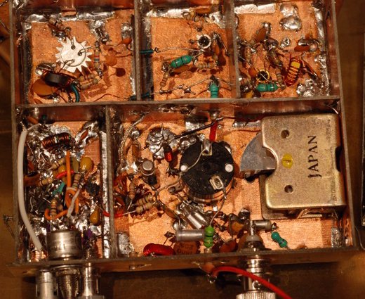
Noise
Blanker Circuit.
This
is a photo of the Noise Reciever.
The blanker is very effective. Noise pulses from power line leakage or RFI
from dirty commutator brushes in kitchen appliances that register S-9 on my S
meter are totally eliminated with this blanker circuit. My wife's old Kitchen
Aid Mix Master is particularly bad and it seems she uses it mostly when I am
trying to copy a very weak DX station, HI. She is a fantastic cook so I dare
not complain.
Noise blankers in commercial ham radios may be
effective when there are few strong signals in the receiver passband, however
in a contest environment where there are many strong stations filling the
receiver passband, severe intermodulation is the result, rendering the
blanker useless. This design does not suffer from thie
problem because the noise receiver is tuned to a freq. far away from the
strong contesting stations. Of course this blanker can only eliminate pulse
noise, which is easy since the noise is very different from the signal you
are trying to copy! What I need now is something for electronic broadband
RFI!
8. Front Panel Layout
Front panel layout plays a big role in how a transceiver feels when
operating. The placement of knobs and switches should all be placed so that
minimal hand movement is required when different bands, modes, and filters
are selected. I use my rig for listening as well as operating events like
hunting DX or contesting. I have arranged the most commonly used knobs and
switches close to the tuning knob allowing one hand operation of the
HBR-2000. For example, the filter selection buttons are just to the left of
the main tuning knob, with the mode selection buttons just below. The RIT/XIT
switch and tuning buttons are just to the right of the main tuning knob. With
this arrangement I do not have to take my hand off the main tuning knob to
change selectivity. I just use my left little finger to select which band
width I want.
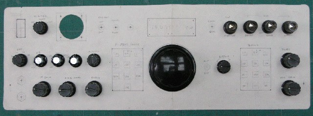
I designed the front panel by making a paper template of the panel. I then
laid all the knobs, switches, the S meter, frequency display and band select
and mode/filter push button units on the template. I moved everything around
until I felt good about the layout. However, I did not make a final decision
until I had thought about it a lot. I thought about the layout during the
day, dreamed about it at night and time after time I sat in front of the
paper layout and visualized how it would feel to operate. When I came up with
the final panel layout I traced around the knobs etc. with a pencil. I then
taped the paper template to the aluminium front
panel and used the template to centre punch the
holes for the different controls and corners of the digital display etc.
Front
Panel Template
After cutting and drilling the holes I sanded the panel with very fine
sandpaper and spray painted with the colour of my
choice. I then used press-on Letraset for the
control labels. After applying the labels I sprayed the panel with clear
lacquer.
It is time consuming to make a front panel that is both eye appealing and
ergonomically functional, however it is well worth the effort.
9. Transmitter 100 Watt
Amp.
Here are a few pictures, I may add comments later.
100
Watt MOSFET Amplifier board.
100 Watt Amplifier Low Pass Filters.
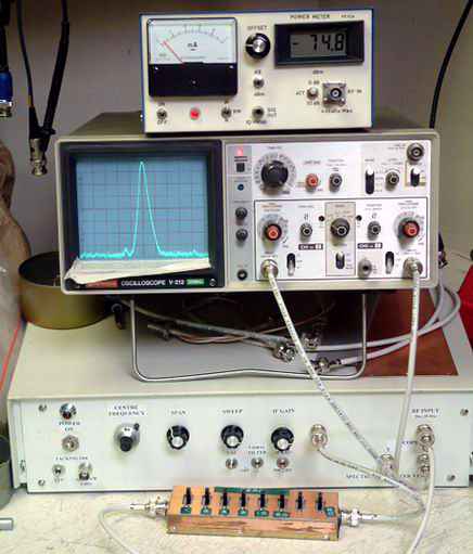
10. Test Equipment
The following picture shows some of the test equipment I built during the
development of the HBR-2000. At the bottom is a step attenuator, the box below
the scope houses the Spectrum Analyzer based on the W7ZOI/K7TAU design
(August 1998 QST) and above the scope is a the Power Meter based on
W7ZOI/W7PUA design (June 2001 QST) with digital read out addition by K3NHI
(May/June 2002 QEX)
Test
Equipment Used.
11. Keeping Records
Whether you decide to build a simple 2 stage transmitter or a full fledged
transceiver, keeping complete and accurate notes and records plays a very
important part in the end result. I used a three ring binder complete with an
index and dividers for keeping circuit diagrams, notes, hand drawn layouts,
pictures etc. for each bulding block in my
transceiver. All the parts are labeled. When making measurements I note the
DC and RF voltages at key points on the circuit diagrams. In some cases a colour photo of the block is included.
If I decided to experiment with a particular circuit and try different
component values and measure the results I used spiral bound note books for
the records. After I decided on the final design of a paricular
circuit or building block, I then made a copy of the final circuit diagram
complete with the measurement results and inserted them in the main 3 ring
binder. By keeping good records I can go back and see what changes I made and
what the results were if I want to use a particular circuit again.
You will be glad you made good notes if your project quits and you want to
find out why, ESPECIALLY if it is a complex and full featured 10 band HF
transceiver.
Conclusion
The receiver section of the HBR-2000 is an absolute joy to use. There are no
unwanted birdies or images, the audio is cyrstal
clear, the IF filters are sharp, plus the AGC has to be heard to be
appreciated. Since completing the transmitter portion of the HBR-2000 I have
sold my old TS-940s and the HBR-2000 is my main transceiver. The many, many
hours spent in planning and building have been well worth while. Sincere
thanks to a special friend and Elmer, who wishes to remain anonymous, who
gave unselfishly of his time to answer my unending questions and Wes, W7ZOI
who offered much encourgement and technical advise.
Published Articles (Copyright
ARRL. All rights reserved, used with permission of the ARRL.)
QEX Mar-06, Perf. QSK QST Mar-06, HBR-2000
73 VE7CA
|