2KW LDMOS AMPLIFIER FOR 144MHZ |
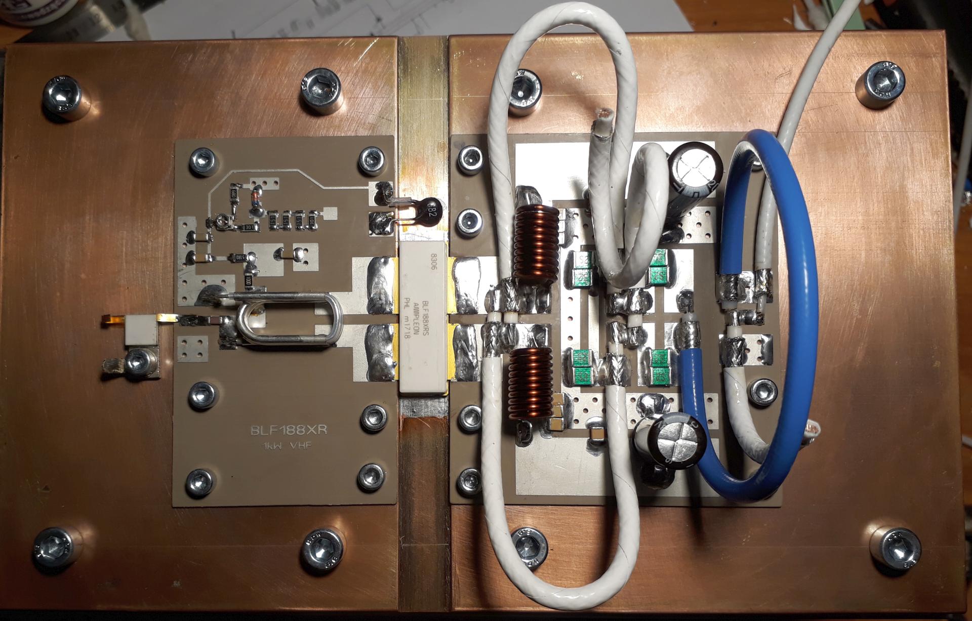
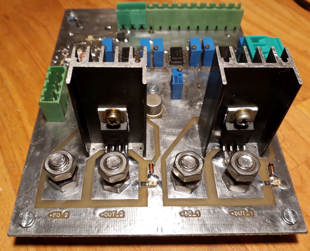
1KW LDMOS PALLET
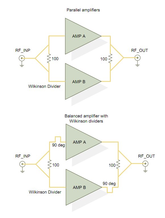
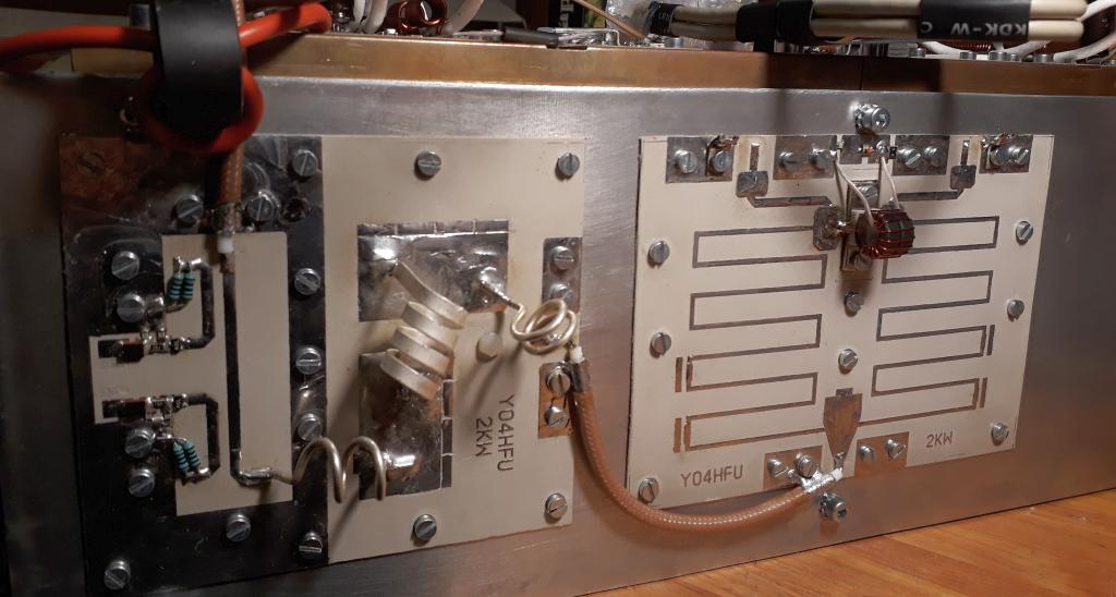
144MHz 2KW LDMOS all mode amplifier using 2 pcs BLF188XR. Both amplifiers are combined using Wilkinson couplers.
The PCB of LDMOS pallet was orderd from Ebay and it is clone of W6PQL project. The price of LDMOS kit was 150$ (transistor not included), bought from "60dbmcom" Ukrainian seller: Ebay link. PCB matterial is ARLON TC-350, FR4 is not suitable for high power at 144MHz.
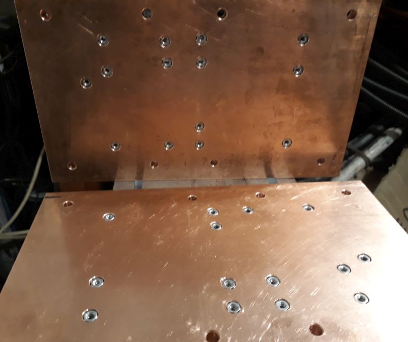
Copper heat spread (200x120x10mm) is home made and heatsink is STONECOLD RAD-A6405A/400 "Y" type 400mm length. It can be order from TME. BLF188XR (BLF578XR) is soldered on the copper spread for best heat transfer.
Several transistors can be used with this kit: BLF578, BLF578XR, BLF188XR, MRFE6VP61K25H. Ampleon's transistor has "XR" marking for eXtremely Rugged device. XR family is able to survieve during extreme load mismatch conditions.
The final version of amplifier use only one piece DPR-2900 at 54Vout and is able to delivery 2.2KW RF Out during EME operation. Typically class AB biased is adjusted for Iq=2A, efficiency 67% at 1KW output (for one pallet).
BLF188 needs aprox 1.88V gate voltage for 2A idle current. Due safety reasons, use other current limited PSU and increase voltage step by step. In same time check ampere meter indication. Output current of PSU must to be adjusted at max. 0,5 Amps. Adjust variable resistor for minimum bias voltage (cursor to GND side). If everything looks good, PSU over current protection can be increased more than 2 Amps and bias adjusted by small steps. SMD variable resistor (200 ohm) can be easily damaged by wrong maneuvering.
LDMOS amplifier has high gain (~27dB) and required input level is less than 3W (35dBm) for 1KW (60dBm) output. Do not overdrive LDMOS transistor, it is very sensitive and will be damaged. Is a good practice to use a pad attenuator between TX exciter and LDMOS PA, less chance of over driving and better return loss (better input SWR).
Maximum output power of a single LDMOS pallet was 1,2KW. Output harmonics at 1KW without LPF are not very bad, 288MHz=-43dBc, 432MHz=-43dB, 580MHz=-53dBc, 725MHz=-45dBc. Better harmonic suppression can be observed at 600W, 288MHz = -55dBc, 432MHz=-48dBc, 580MHz=-52dBc, 725MHz=-58dBc. Anyway output LPF needs to be installed.
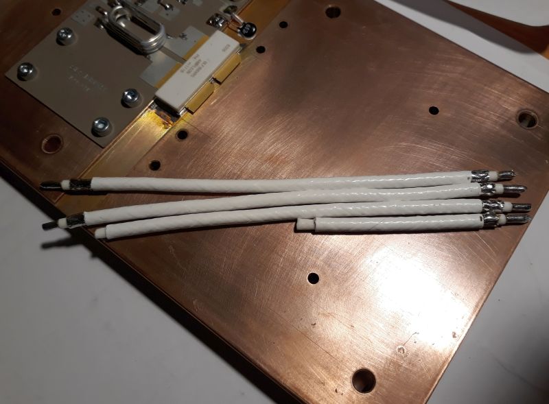
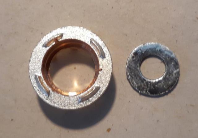
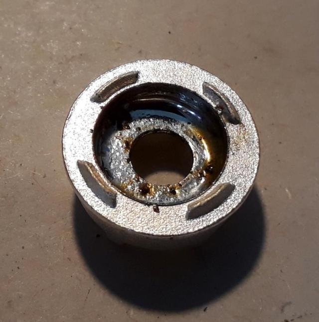
Coaxial cable provided for output balun is a blue PTFE 50 ohms 0.141", maybe RG402. At full power, it is very hot and better to be replaced using RG400/RG142. White coaxial cable is TC-12 (12,5 ohms), take care during length preparation because is expensive and difficult to find. Output capacitors (35pF/15pF) are made using same TC-12 coaxial. Capacitance value was found higher, almost +2pF more than schematic values, length according W6PQL specifications. No improvement was observed during capacitance adjustment for accurate 15pF/35pF. So cut all coaxial cables using below dimensions recommended by W6PQL. All lengths measured between shield to shield sides:
![]() TC-12 white PTFE baluns: 2pcs x 120mm
TC-12 white PTFE baluns: 2pcs x 120mm
![]() RG402/400/142 output balun: 1pc x 171mm
RG402/400/142 output balun: 1pc x 171mm
![]() 35pF capacitor TC-12 coaxial: 1 pc x 110mm
35pF capacitor TC-12 coaxial: 1 pc x 110mm
![]() 15pF capacitor TC-12 coaxial: 1pc x 50mm
15pF capacitor TC-12 coaxial: 1pc x 50mm
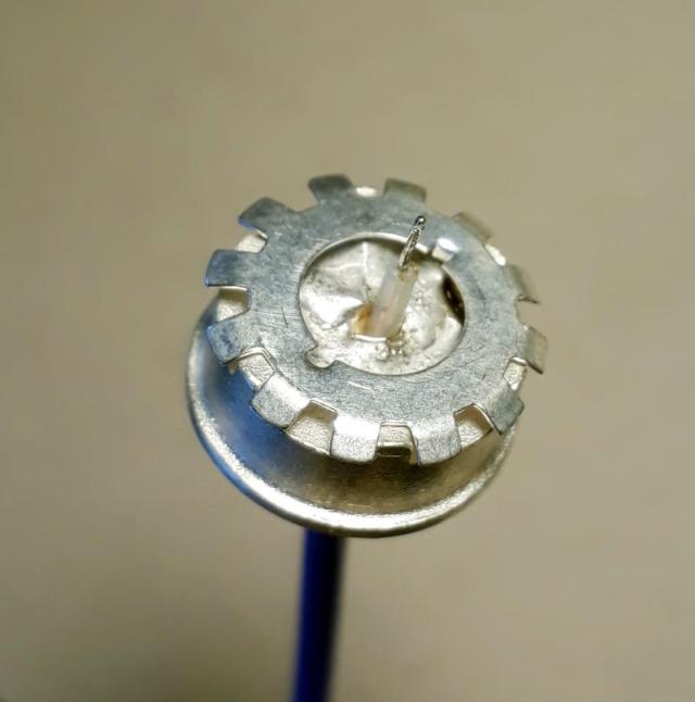
Coaxial cable capacitors can be replaced with good results using other kind of PTFE coaxial. I made some experiments using 50 ohms RG402, required length is higher than TC-12. For 15pF are necessary 155mm of RG402 0.141". Try to avoid resonance of coaxial cable.
![]()
![]() BLF188XR 144MHz 1KW pallet
BLF188XR 144MHz 1KW pallet
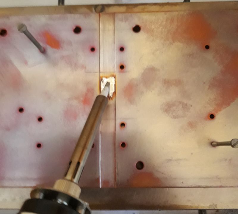
![]() Soldering preparation
Soldering preparation
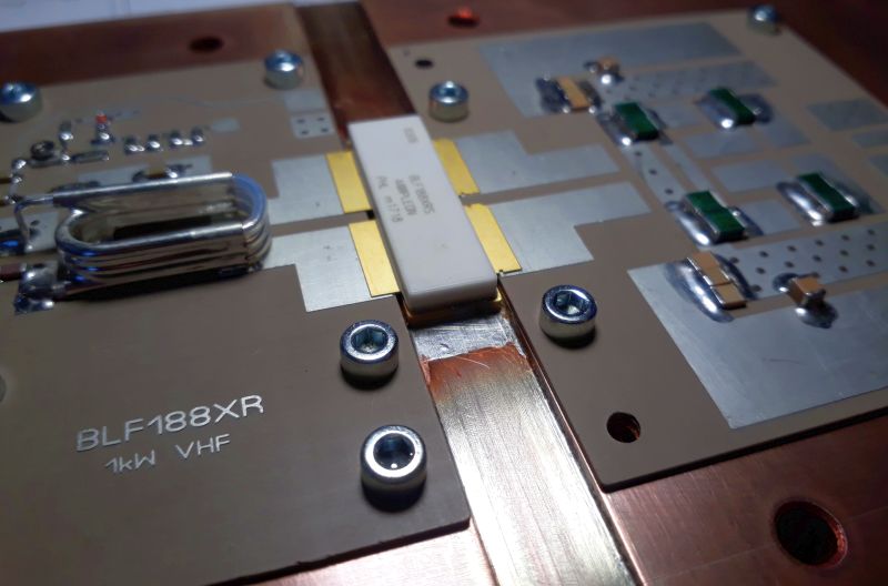
![]() LDMOS soldered
LDMOS soldered
![]() TC-12 PTFE baluns and capacitors
TC-12 PTFE baluns and capacitors
![]() Copper heat spread
Copper heat spread
![]() Test 1100W
Test 1100W
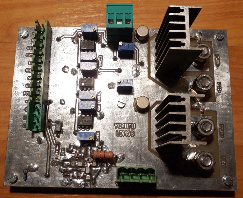
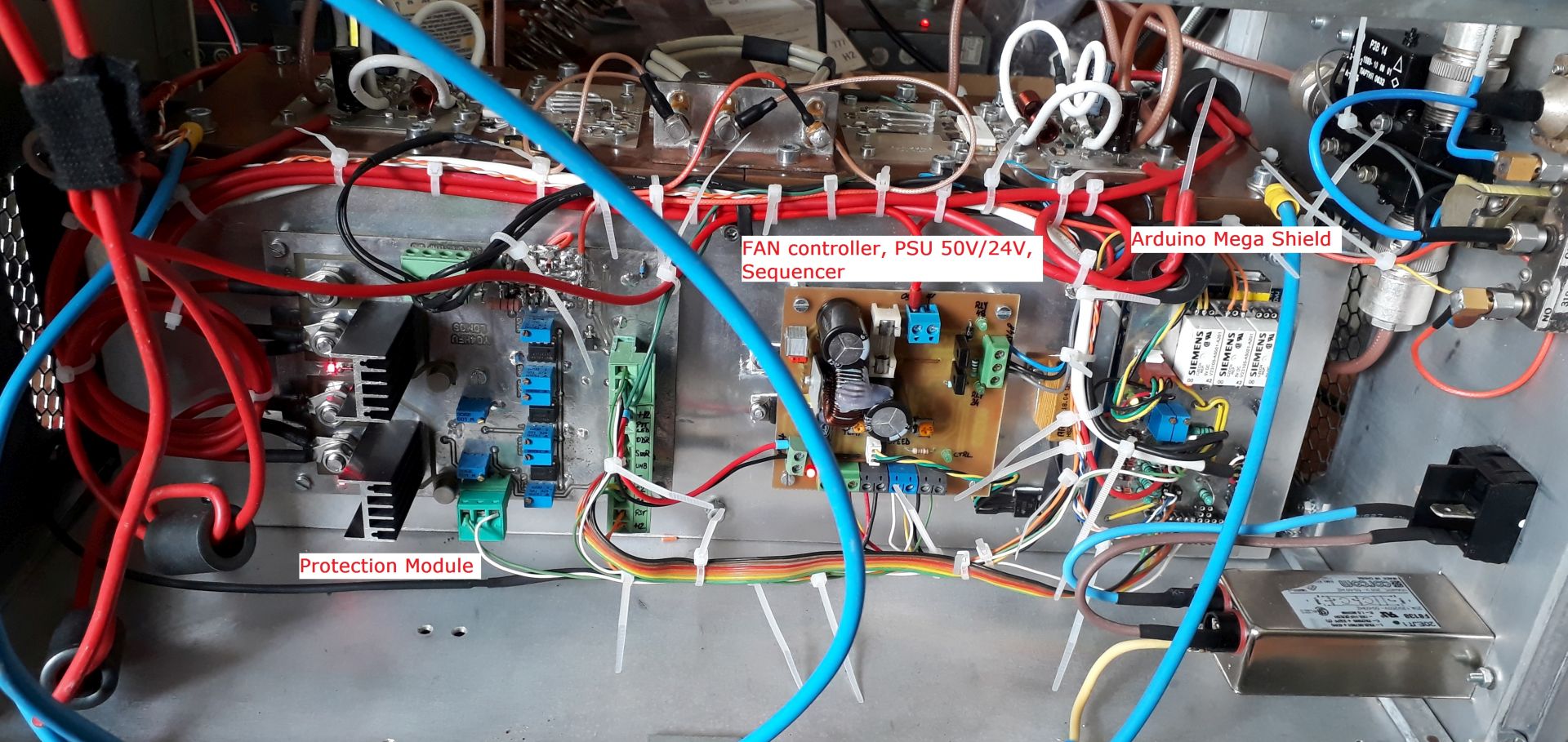
PROTECTION MODULE
During bench experiments, extreme mismatch condition was tested... Output short circuit occurs at full power due voltage breakdown inside of 20pF air capacitor connected between output and ground. After that, shield connection of output coaxial was broke by mechanical tension between pallet and Bird wattmeter. BLF188XR has survived without any SWR protection. Don't try your luck!
Before to attemp my first combined 2 x 1KW amplifier, i designed a properly protection module. Next requirements have been followed:
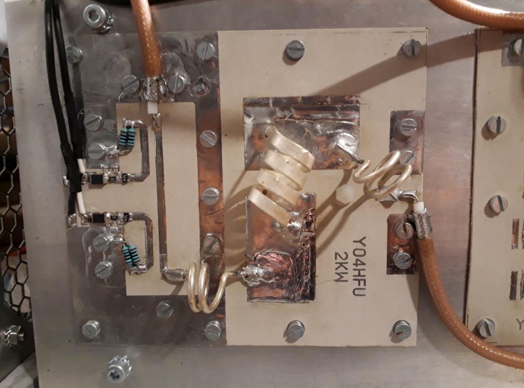
![]() Overdrive protection. PIN diode used for fast response time. No relay or zenner diodes.
Overdrive protection. PIN diode used for fast response time. No relay or zenner diodes.
![]() SWR protection
SWR protection
![]() Unbalance detector in case of one LDMOS pallet failure
Unbalance detector in case of one LDMOS pallet failure
![]() Overheating protection
Overheating protection
![]() Overcurrent detection for each amplifier. Current indication on front pannel.
Overcurrent detection for each amplifier. Current indication on front pannel.
![]() Full analog protection, fast and without special components. Every latched alarm indicated by LED.
Full analog protection, fast and without special components. Every latched alarm indicated by LED.
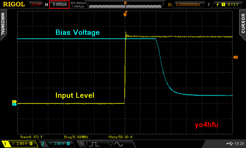
All failures lead to disable RF Input / BIAS voltage / +50V supply. In my opinion overdrive protection and high SWR are the most critical. Response time between overdrive and RF input disconnection is less than 15uSec. The response time can be improved by replacing LM393 comparator with very fast comparator IC (TLC372) . In case of protection activation, output of VHF transceiver is connected to a 50 ohms true dummy load, response time 10uSec. The response time for overdrive is imposed by constant time of RC filter connected at detector output. SWR input can response in less than 2uSec, measurement made without external diode detector.
Good returns loss (> 28dB), low insertion loss (0,25dB) and enough isolation (>30dB) were achieved using PIN diodes biased at 100mA. I didn't made IMD measurements but good values are expected.
Any low distorsion high power PIN diode is suitable. For example you can use MA4P series (MELF package) or UM9401 (through hole package).
Power supply line is switched by two pieces Infineon BTS50085. Every smart high side high current power switch is connected between +50V and LDMOS amplifier. Small heatsink installed are recommanded in case of full power and heavy Tx-Rx duty cycle. BTS50085 internal resistance is ~7mOhms, this means 6W heat dissipation at 30A/50V. Current sensing pin is buffered and provides load current indication. No shunt resistor and linear response of sensing pin are few features of BTS50085 wich can be replaced by BTS660 obsolete device. PTT signal is used to switch OFF BIAS voltage and RF EXCITER.
![]()
![]() Protection Module schematic revison 1.2 - 40uSec
Protection Module schematic revison 1.2 - 40uSec
![]() ProtectionModule revision 1.3 - more faster <15uSec
ProtectionModule revision 1.3 - more faster <15uSec
![]() Overdrive Response time for version 1.3
Overdrive Response time for version 1.3
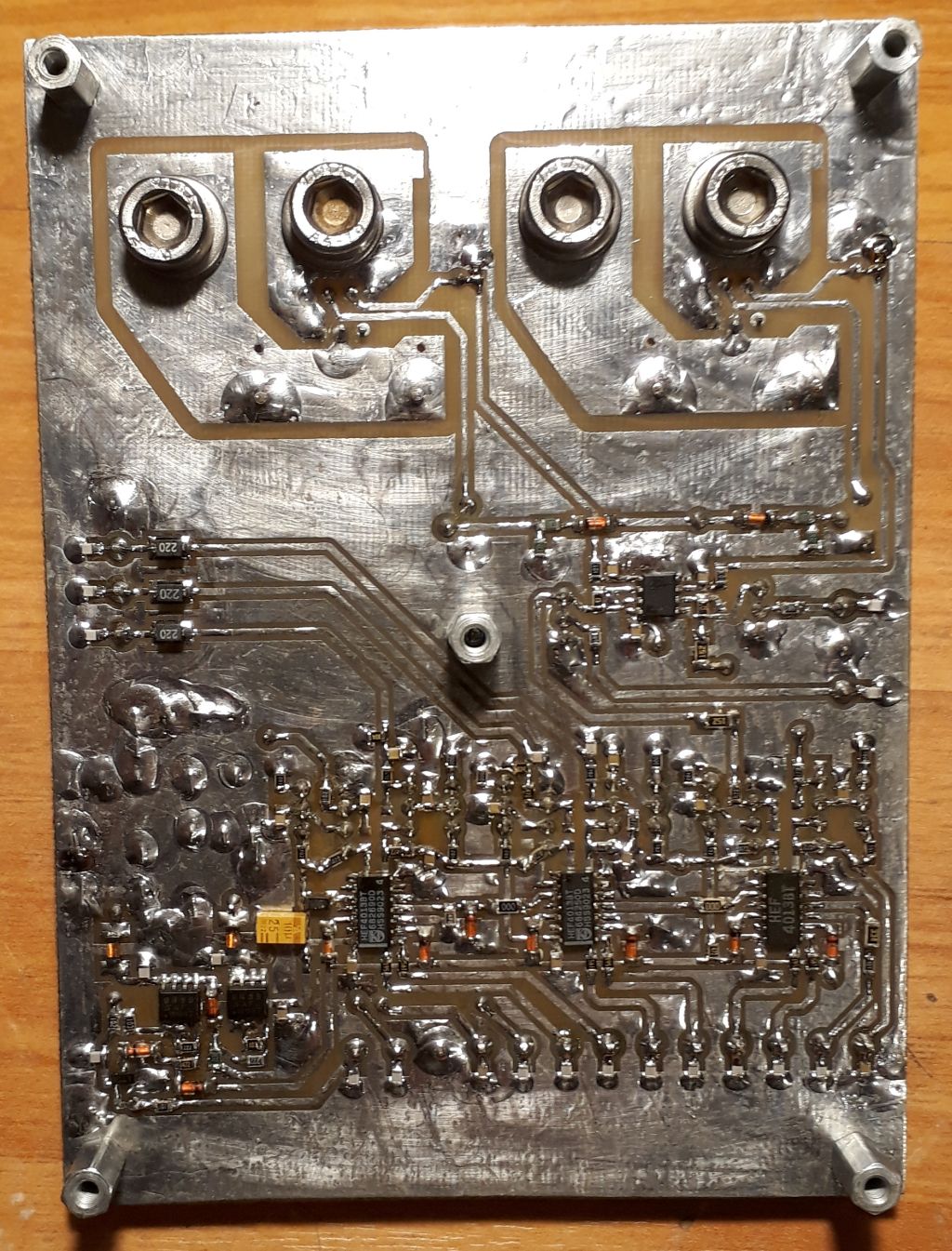
![]() Protection Board Top
Protection Board Top
![]() Protection Board Bottom
Protection Board Bottom
![]() BTS50085 PROFET switch
BTS50085 PROFET switch
![]() PCB rev 1.1 (for home made)
PCB rev 1.1 (for home made)
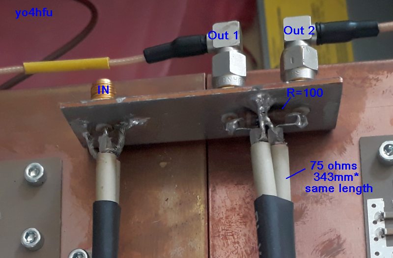
WILKINSON SPLITTER / COMBINER
Input power is divided using a Wilkinson splitter. Transmission lines were made using 75ohms coaxial cable. Length has (Lambda/4)*V, for common polyethylene cable V=0.66 length at 144,300MHz will be 343mm. High isolation was achieved by trimming the cable +/- 1mm during final installation.
Ballast resistor has 100 ohms/0,5W carbon resistor with low parasitic inductivity. Use short connections and coaxial shield divided in two bundles. Here you can see coaxial cable arrangement. Excellent performances were obtained. Below values are maintained only if the input impendence is close to 50 ohms. Also 3dB attenuators were installed between splitter outputs and LDMOS pallet inputs in order to improve return loss with +6dB.
![]()
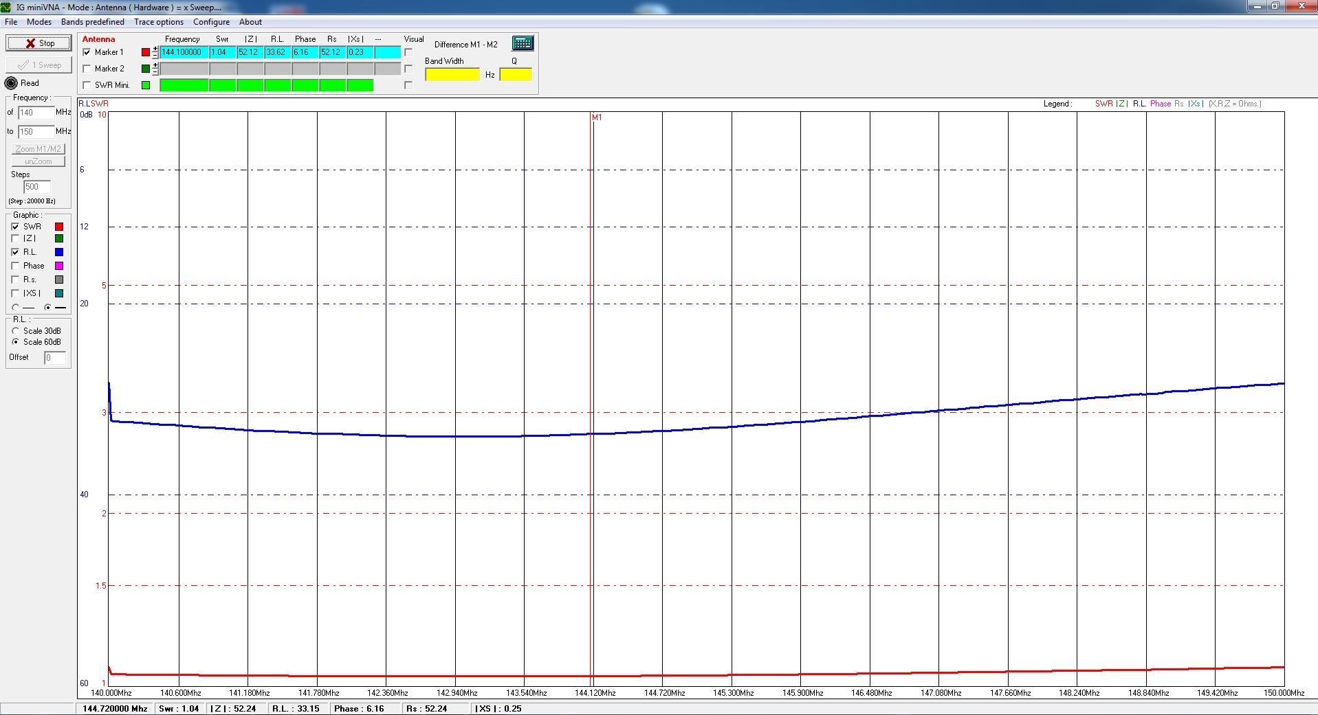
![]() Isolation between output ports
Isolation between output ports
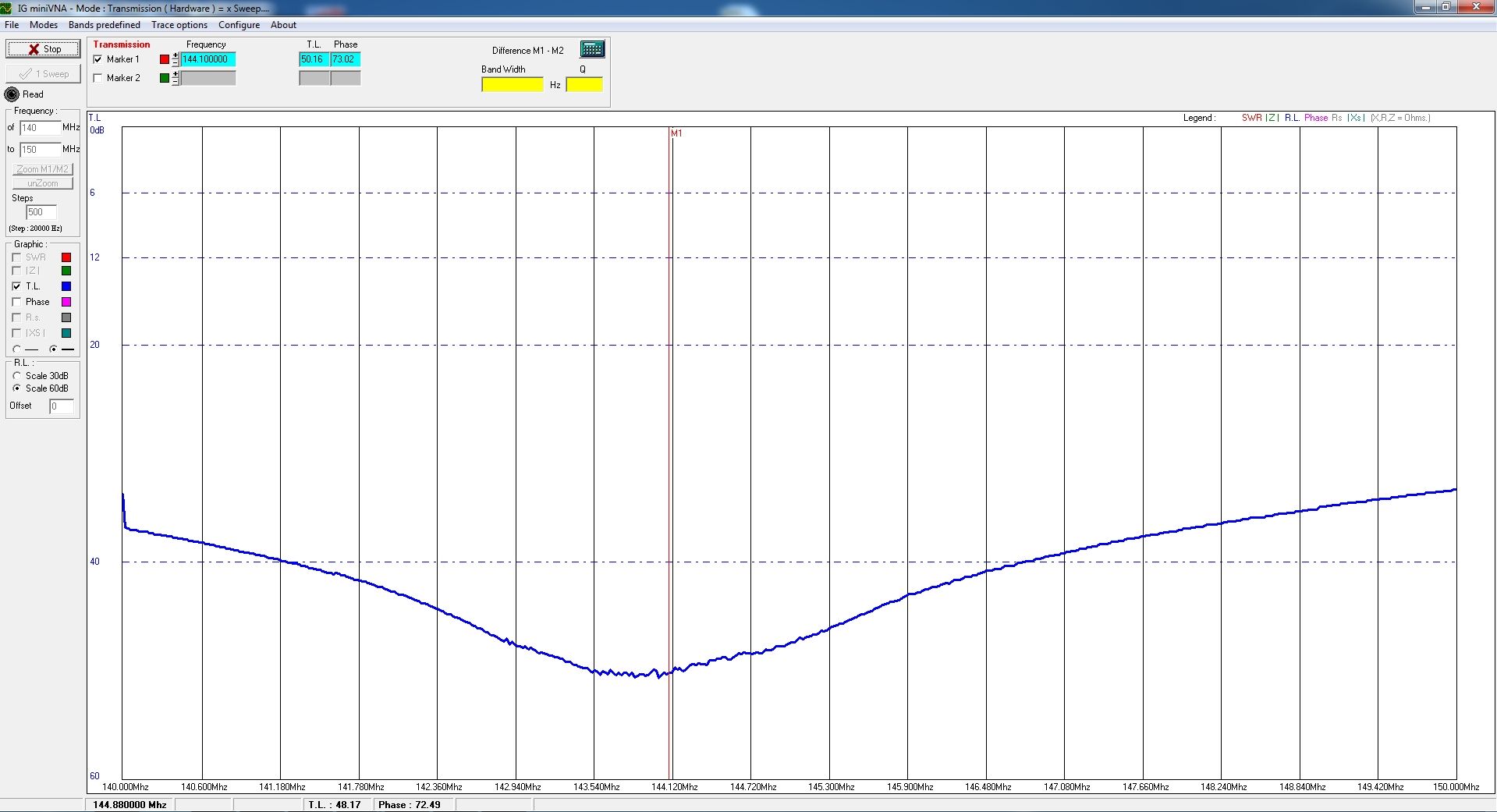
![]() Return Loss Input
Return Loss Input
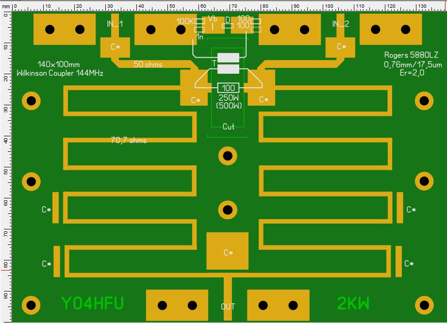
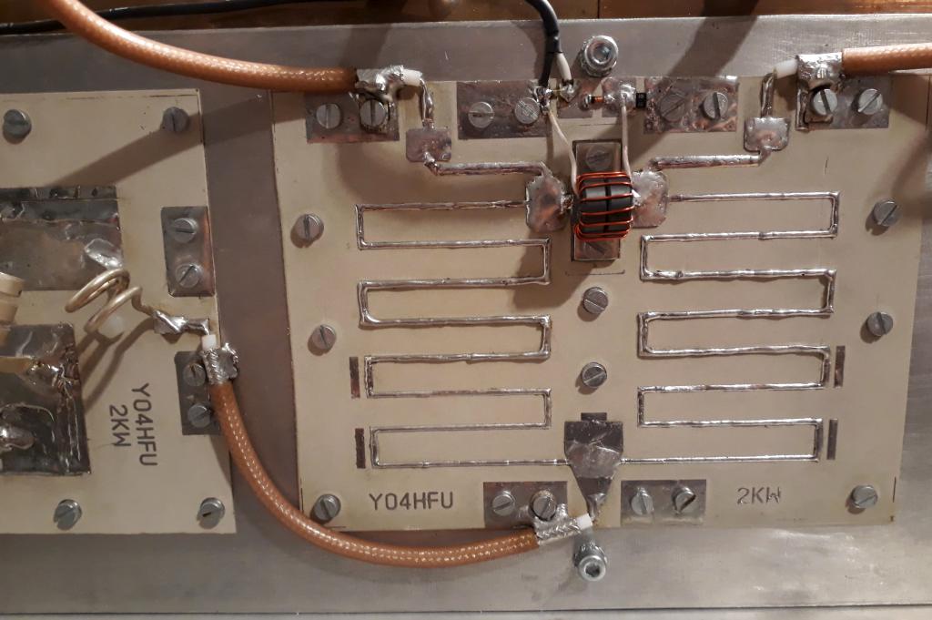
Output Wilkinson combiner (coupler) is built using PTFE PCB. I made some experiments using coaxial cables but was difficult to adjust length of cables for best performances. Microstrip line technique can be fine adjusted using small pieces of copper sheet. Input/output ports needs to be capacitive compensated for best return loss. Try to find a reasonable balance between return loss and isolation. PCB drawing was updated to revision 2, but fine adjustments are still required by trimming compensation capacitors C*.
Microstrip line dimensions were calculated using "TxLine2003" software for double sided substrate Rogers RT/Duroid 5880LZ, 0,76mm, 17,5um, Er=2. Microstrip line 70,7 ohms has no mitered corners because I'm tried to avoid narrow width, current capacity of 1,41mm microstrip line is not so big. Practical results have shown that the line does not warm up, so no problem if you like mitered corners (LE: midlle area of 70 ohms microstrip becomes very hot during operation at full power. Microstrip line requires tinning in order to increase the current capability). Mitered corners of stripline can reduce reactive impendence of microstrip line. Example of Wilkinson microstrip line corners used by LARCAN TV amplifier.
Ballast resistor has 100 ohms/250W. In case of one LDMOS failure at 2KW full output, the resistor needs to absorb 500W (6dB or 1/4 of output power). I use 250W resistor because I don't expect to run only one LDMOS pallet in case of failure (in this situation available output power will be 500W). Dissipated power across resistor is the best indicator for unbalance operation due to LDMOS failure, power supply/excitation missing for one stage or any phase/gain unbalance. Voltage step down transformer (13:1 ratio) is used to monitor RF voltage across resistor. Maximum 225Vrms is expected across resistor. Secondary voltage is rectified by 1N4148 diode. Unbalance DC signal is connected to protection module. Unbalance fault triggers OFF the RF input and power supply voltage. Protection response is very fast, less than 15uSec and ballast resistor can handle full power without to have 500W rating. Step down transformer is built using 2 pieces Amidon FT50-61 toroid core. Primary side has 13 turns of 0,4mm wire, secondary side 1 turns PTFE insulated wire. Any other VHF ferrite can be used if the coupler performances remain almost same during connection/disconnection of toroid transformer.
Unbalance test done: one LDMOS pallet disconnected during operation at 200W. Output power dropped to 50W (-6dB) and unbalance DC voltage goes up to 5V ( 70Vrms across 100 ohms resistor).
![]()
![]() PCB Wilkinson Coupler top layer
PCB Wilkinson Coupler top layer
![]() PCB component position
PCB component position
![]() Final version of output coupler
Final version of output coupler
Coaxial cable between splitter/combiner and both LDMOS pallets have same length, otherwise the signals will be unequally delayed and phase ballance affected. Also I made experiments using "balanced amplifier" configuration. Balanced configuration is recommended due to small interaction between amplifiers. Two pieces for 90 degrees delay lines were built using L/4 50ohms coaxial. Unfortunately the result was not very good. The maximum output power was 1600W and unbalanced voltage was higher than parallel operation. Maybe the issue is due to small unbalance of gain introduced by different insertion loss of coaxial cables. For input delay line i use RG178 and for output delay line RG402. Both cables have same velocity coefficient V=0,7.
Harmonic level at 2KW CW without LPF: 288MHz=-48dBc, 432MHz=-43dBc, 580MHz=-60dBc, 725MHz=-50dBc. Even harmonics are better rejected than a single LDMOS stage, improvement due to parallel operation.
Overall efficiency, class AB Iq=2A, both amplifiers combined (230V AC consumption vs RF output power): 49% for 1KW; 58% for 1,5KW; 68% for 2KW. Efficiency of PSU Delta DPR-2900 is 96%. So if you need 1KW or less, better use only one piece LDMOS pallet for best efficiency.
LOW PASS FILTER & DIRECTIONAL COUPLER
The LPF has 5 poles is capable to clean the output spectrum of LDMOS amplifier. Harmonics are less than 65dBc according SA monitoring at 2KW (span 50MHz/division, vertical response 10dB/division).
LPF will be tuned for best input return loss between 144-146MHz by adjusting the lenght of the coils. For best results you can use VNA or directional bridge. Also alignament can be done using a powermeter/SWR meter but with less accuracy. PCB capacitors have 20pF and dimension are calculated for PTFE pcb 5880LZ, 0.76mm, Er=2. PCB capacitors are designed according online calculator "Capacitance without edge effect". Some pads are provided for fine adjustements of 20pF capacitors. For coil use only silver plated wire, 2mm minimum diameter and try to avoid mutual coupling. First and last coil (2 turns) are wound in opposite directions. Fine adjustements of coils will be done during operation for maximum output power and efficiency.
LPF measurements:
Insertion loss ~0,1dB; input RL >35dB.
Response: -3dB/214MHz; -20dB/288MHz; -41dB/432MHz; -55dB/576MHz.
Microstripline directional coupler has ~50dB coupling factor and pickup loops are capable of >27dB directivity. Do not use SMD resistors for 50 ohms microstrip line terminations. Best results are achived with 1% metal film resistors. Keep the ground connection inside of the loop and body resistors away from ground plane, otherwise the directivity is very poor (only 5-6dB). Connects the spectrum analyzer or RF voltmeter in place of detector diode. Change resistors positions for lowest value of reverse signal. Then change antenna/input port of directional coupler in order to check the forward pickup line using same technique. Connect the diodes and check the directivity, DC voltage ration between REV/FWD will better than 7,5 (>17,5dB). All measurements are done using good quality 50 ohms dummy load. If is possible use vias between top/bottom ground plane or at least M3 screws. Forward voltage is around 2,8Vdc / 2KW output.
![]()
![]() Top side layer of LPF
Top side layer of LPF
![]() Top side view - component position
Top side view - component position
![]() Final version of LPF
Final version of LPF
![]() View of output Wilkinson and Low pass filter board
View of output Wilkinson and Low pass filter board
![]() REW-14 coaxial relay, connector modification for small coaxial 0.141". Photo #1, #2, #3, #4
REW-14 coaxial relay, connector modification for small coaxial 0.141". Photo #1, #2, #3, #4
FAN SPEED CONTROL, TX-RX SEQUENCER, 50V/24V STEP DOWN PSU
Cooling fans speed are adjusted according heastink temperature. Speed is maximum during TX period. Regulator circuit is simple, using discrete transistors.
Tx-Rx sequencer is used to protect coaxial relays and to avoid "hot" switching. When PTT is engaged, first event is to switch both coaxial relays (input and output). After aprox. 100mSec delay, LDMOS bias voltages are aplied and both transistors start to take idle current. Of course, bias voltages are disable if protection module has an alarm event.
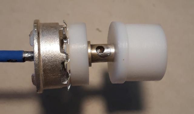
All low power circuits are supplied by 12V. Fans and output coaxial relay (russian REW-14) are supplied with 24V. Input relay is a SMA version with 48V coil (very cheap on Ebay). This relay is supplied from 50V bus. Output circuit of sequencer can be modified for any 12/24/48V coaxial relay. The topology of sequencer is almost same with W6PQL schematic or Handbook examples.
Because is quit difficult to step down 50V to 24V without to using a big heatsink, i choose switching mode regulator solution. LT1074HV 100KHz step-down regulator is able to delivery 5A. Maximum input voltage is 64V. During my first experiment, i wasn't able to obtain more than 1A and efficiency was poor (LT1074 very hot). The problem was fixed by replacing 100uH output coil . I don't know the material of ring core, i found it in my junk box. Check LT1074HV datasheet in order to select the coil. Examples: 100uH, Wurth Elektronik 744114, RADIOSPARE 617-1338; COILTRONICS #50-2-52; PULSE ENGINEERING #PE-92114; HURRICANE HL-AK147QQ or other 50-100uH coil designed for 100KHz buck regulator. Switching noise is low, I didn't observed interference with 144MHz transceiver.
![]()
![]() Schematic of Fan speed regulator / PTT Sequencer / 24V; 12V PSU
Schematic of Fan speed regulator / PTT Sequencer / 24V; 12V PSU
![]() PCB component position
PCB component position
![]() PCB bottom
PCB bottom
LED POWERMETER WITH PEAK HOLD FEATURE
Reading of output power is accomplished with a full analog LED bargraph. Forward DC voltage from directional coupler is amplified and then displayed using two pieces LM3914. Both ICs are cascaded to drive 20 pcs LED, every LED represents 100W step. The challenge was how to designed a simple peak hold function around LM3914. Peak hold can obtained by switching LM3914 bar/dot pin and release time of input circuit. Switching speed is aprox. 200Hz, enough to avoid flickering of bargraph. Calibration is made at full indication (2KW) and 500W using 2 variable resistors LOW/HIGH Scale. Linearity is good between 500-2000W. Peak hold option is very useful for SSB monitoring.
![]()
![]() Schematic of LM3914 Peak Hold Bargraph
Schematic of LM3914 Peak Hold Bargraph
![]() PCB component position
PCB component position
![]() PCB layout
PCB layout
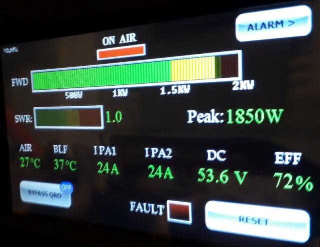
ARDUINO HMI
Above modules are able to operate standalone without any uC controller. Relay sequencer, fan control, protection module, output LED bargraph were designed for small price, simple to operate and adjust.
A modern look can be achieved by using a touch screen (HMI = human machine interface) interconnected with the protection module. LED bargraph powermeter is not more required.
Additional items:
- Arduino Mega 2560
- Homemade Arduino Shield
- 4D uLCD TFT 4,3" with resistive/capacitive touch screen
Interconnection diagrams or other details are not available.
![]()
![]() View of modules during QRO construction
View of modules during QRO construction
![]() Arduino Mega software - Visuino software enviroment
Arduino Mega software - Visuino software enviroment
![]() 4D uLCD files - Workshop 4 IDE Visi-Genie software
4D uLCD files - Workshop 4 IDE Visi-Genie software
![]() Arduino Shield PCB - SprintLayout files
Arduino Shield PCB - SprintLayout files