Receiver Module
Schematics
Sheet 1 Sheet 2 Sheet 3 Sheet 4 Sheet 5
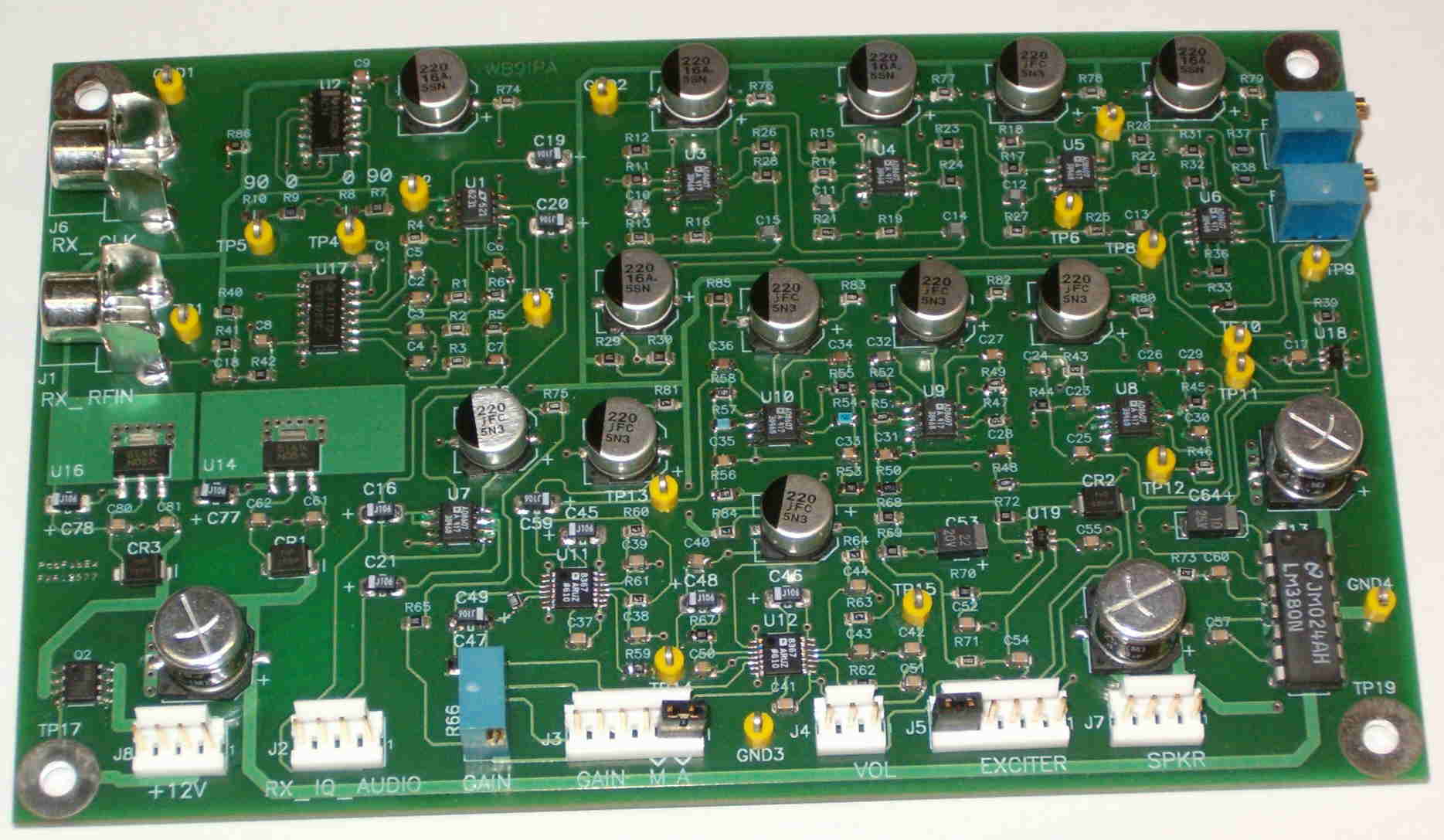
PCB
Layout
Features
The
receiver module is a single-signal, direct conversion design, which is capable
of receiving Single Sideband (SSB), AM and CW signals over a range of <100
KHz to 30 MHz. Receiver adjacent
channel selectivity is provided by an audio filter chain of a four pole,
highpass filter followed by an eight pole, lowpass filter. Automatic Gain Control (AGC) is provided to
maintain a constant audio level despite wide variations in RF signal level. The audio output amplifier is capable of
driving >1 Watt into an 8 Ohm loudspeaker, providing sufficient audio drive
level for use in noisy environments.
This module does not provide local oscillator generation or receiver
front end selectivity; these functions are provided by the OSC_FILTER module.
Specifications
DC
supply input: 10-15 VDC
Operating
temperature: 0 – 70 C
Receiver
MDS: -130 dBm
Two-Tone
Third Order Dynamic Range: 102 dB
Operating
frequency range: <100 KHz – 30 MHz
Undesired
sideband suppression: >40 dB
Modes of
operation: SSB, CW, AM (by zero beat
method)
Local
oscillator output level: TBD
PCB
dimensions: 3.9 x 6.25”
Theory
RF signals, which have been
previously band-limited by filters on the OSC_FILTER board, enter the receiver
module via connector J1. From here, the
RF is passed to U17, which is a dual, single
pole four throw solid state analog switch, configured as a Quadrature Sampling
Detector (QSD), also known as a Tayloe detector. For an explanation of how the QSD operates, please refer to this article by Mr. Tayloe, as well
as the patent for his circuit. C2, C3, C4 and C5 are chosen such that, when
combined with a 50 Ohms signal source impedance from the RX INPUT, each forms a
lowpass filter with a cutoff frequency of approximately 7.9 KHz. The signals developed across C2, C3, C4 and
C5 are then amplified and further lowpass filtered in U1A and U1B. Each of these amplifiers has a lowpass
cutoff frequency of approximately 16 KHz.
After
the signal has been detected in U17, U1A and U1B generate two audio
signals: RX_I_AUDIO and RX_Q_AUDIO.
These signals are identical in their information content and amplitude,
but, they are separated in phase by 90 degrees. A portion of these signals is sent to buffer amplifiers U7A and
U7B for use in offboard Software Defined Radio (SDR) experiments, or other
uses. RX_I_AUDIO and RX_Q_AUDIO are
also sent to the audio phase shift circuits (sheet 2) for further processing.
Local
oscillator drive for the QSD is provided by U2A and U2B, which form a quadrature counter. RX CLOCK enters the receiver module at 4X
the operating frequency and is divided by U2A and U2B to produce four separate
signals at the operating frequency and separated by 90 degrees. R7, R8, R9 and R10 are 0 Ohm jumpers which
are selected to be installed as needed to obtain the correct sideband selection
sense. Only one pair of resistors (R7
and R9 or R8 and R10) should be installed at any time.
U3, U4 and U5 form a wideband
audio phase shift network which is configured identically to that in the
exciter module. The network was
designed using the J-TEK
Allpass Filter Designer to provide a 90 degree phase
differential over the range of 200 – 4000 Hz.
The passive components used in this network are identical to those in
the exciter.
A
difference amplifier (U6A) takes the difference
between the audio signals at the outputs of U5A and U5B to extract the upper
sideband (USB) audio signal.
Potentiometer R34 is used to adjust the amplitude balance of the two
signals, in order to obtain the deepest null of the unwanted lower sideband
(LSB) possible.
U6B is
configured as a summing amplifier, which sums the output voltages of U5A and
U5B to recover the LSB audio signal.
Potentiometer R35 adjusts the amplitude balance of the two input signals
to null the undesired upper sideband signal.
The
desired sideband audio signal is selected by means of U18, a solid state switch. Control of U18 is by means of a front panel
switch with USB a logic high (or open) and LSB with a logic low (or
ground). The same signal controls
sideband selection in the exciter. This
signal is compatible with 5 volt logic levels, opening the possibility of
control via a microcontroller port pin.
The
selected sideband audio (RX_SELECT_AUDIO) passes into a four pole, highpass,
active filter consisting of U8A and U8B. This filter has a cutoff frequency of 300
Hz.
The
signal next passes through an eight pole lowpass filter consisting of U9A, U9B, U10A and U10B. This filter has a cutoff frequency of 2400
Hz.
While
the filters in the receiver appear similar to those in the exciter, they have
quite different response characteristics.
In the first version of this receiver, both the high and lowpass filters
had Tchebychev responses, identical to those in the exciter. The advantage of the Tchebychev response is
that it has a very sharp roloff beyond the cutoff frequencies. Unfortunately, a negative attribute of the
Tchebychev filter response is phase distortion that occurs throughout the
passband, which causes received atmospheric noise to have a very annoying
sound, as well as excessive ringing, which makes CW signals difficult to
copy.
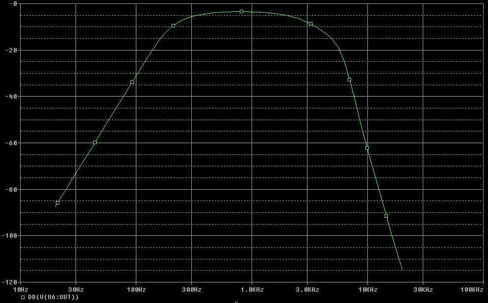
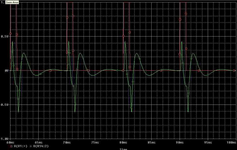
In the
end, another filter was designed which has a near linear phase response. While this filter has a more gradual rolloff
outside the passband, the sound is much more pleasing to the ear. A simulation of the amplitude versus
frequency can be seen here, and a simulation of
filter pulse response can be seen here.
These
filters were designed with the use of the TI Filter Designer,
available as a free download from Texas Instruments.
U11 and U12 for a variable gain
amplifier (VGA) which provide a maximum gain of about 90 dB to the receive
signal path. U12 contains a detector
which converts the output signal to a varying DC voltage which is proportional
to the RMS value of the signal at the output of U12. This proportional DC voltage is applied to the gain control pins
of both U11 and U12, providing a means automatic gain control (AGC) of the
received signal. It is recognized that
there are times that automatic gain control is not desired; for that reason,
two methods of manual gain control have also been provided.
A short
across pins 1 to 2 of J3 will complete the AGC loop, causing AGC action to
occur. Putting a short across pins 2 to
3 of J3 allows the gain to be controlled by means of a voltage applied to pin 5
of J3. This voltage can be obtained R66
(if installed), or, by the use of an external 10 K Ohm potentiometer connected
to pins 4, 5 and 6 of J3.
Capacitors
C47 and C49 control the time constants of the AGC system. Increasing capacitance increases both the
attack and release times. The values
shown appear to be good starting values for SSB operation. See the AD8367 datasheet for
more details.
LEVELLED_RX_AUDIO
from the AGC amplifiers is next sent offboard to the volume control, which is a
10 K Ohm potentiometer. This
potentiometer should be a log taper unit, if possible.
When the
audio returns to the board, it next goes to U19, a solid state switch which
selects receiver audio, or TX_SIDETONE from the exciter board based on the
level of the /PTT line. When /PTT is
high (or open), receive audio is selected.
Conversely, when /PTT is low (or ground), TX_SIDETONE is selected.
The
audio signal from U19 is passed to audio power amplifier (AFPA) U13
where it is amplified to a level suitable for driving a loudspeaker. A snubber network, consisting of C60 and R73
prevent oscillation of U13. Amplified
audio is capacitor coupled to J7 for connection to an offboard loudspeaker. The loudspeaker should be rated for 8 Ohms
and capable of dissipating a minimum of 1 Watt.
Main
power, in the range of 10 – 15 VDC enters the board through J8. Q2 is a P-channel MOSFET (IRF7416), which provides
protection of the module circuits in the case reverse polarity main power is
applied. The use of a P-channel MOSFET
provides less voltage drop than a series diode and does not result in a blown
fuse as would be the case with a parallel protection diode.
The
polarity protected supply voltage is applied to linear regulators U14 and U16
to provide regulated 5 VDC to the +5V and +5VD rails, respectively. Diodes CR1 and CR3 provide protection for
their respective regulators when power is removed from the module.
When
power is removed from the board, energy stored in capacitors on the +5V and
+5VD rails will attempt to discharge through the regulators. Diodes around the regulators provide a path
for this energy to safely discharge, avoiding damage to the regulators.
Separate
LM1117 regulators were provided for the +5v and
the +5VD rails not for noise isolation, but rather, to provide more choices for
the component to be used in U17. U17 is
an SN74CBT3253D, and is used in
the QSD. This part is available in both
3.3 and 5 volt versions. The LT6231 used in the following
stage will operate from 3.3 or 5 volts, as-is.
Powering the +5VD from a separate regulator allows the use of either the
3.3 or 5 volt versions of U17 by simply changing regulator U16 to the
appropriate type.
Bill of Materials
The Bill
of Material (BOM) is provided in three different formats. Excel format is ready for use directly in
Microsoft Excel. HTML format can be
viewed directly on the screen if you do not have Excel or other spreadsheet
software. CSV format can be used by
most spreadsheet software, including Microsoft Excel and others. Here is an explanation of the columns:
Column Label Meaning
A NI? NI = Component not installed
B Pattern Name PCB component pattern
C Ref Des Component reference
designator
D Device Component type
E Val Component value
F Wat Component rating in Watts (if
applicable)
G PCT Component tolerance
H Volt Component Voltage rating
I PMFR Primary manufacturer
J PMFR P/N Primary manufacturer part
number
K P Vendor Primary Vendor (Note: digi = Digikey)
L P Vendor P/N Part number used by the primary vendor
M SMFR Secondary manufacturer
N SMFR P/N Secondary manufacturer part
number
O S Vendor Secondary Vendor
P S Vendor P/N Secondary P/N
Important
note:
The
listing of any vendor or manufacturer in this Bill of Materials does not in any
way constitute any endorsement of any vendor or manufacturer. Vendors, manufacturers and their part
numbers are listed soley for convenience of the builder. The information presented in this Bill of
Materials may contain errors; the author assumes no liability for the accuracy
of the information contained herein.
The user assumes all liability for the use of any information presented
in this Bill of Materials.