IN3OTD's web site
...under perpetual construction.

Hermes-Lite SDR
The Hermes-Lite SDR is "a work in progress to create a low-cost software defined radio HF transceiver based on a broadband modem chip and the Hermes SDR project", as described by its designer, Steve Haynal, KF7O.
I have been following its development for some time and initially build an Hermes-Lite v1, on which I did several measurements and experiments in order to understand its potential and limitations.
This page contains some notes and measurements on this first prototype.
RX input transformer
The AD9866 ADC has a nominal input (differential) impedance of 400 Ω so a transformer is needed to adapt it to the usual 50 Ω.
This transformer is wound on a BN-43-2402 core, with 5 turns on the low-impedance side and 14 turns with a center tap on the high-impedances side
in total 21 turns are needed and to make all these fit into the small core apertures a rather thin wire (0.2 mm diameter) has to be used, together with some patience and a wooden toothpick to compact the turns while building the windings.
Here is a detail of the transformer showing that no space for more turns is left:
")
Here is the transformer ready to be measured with a VNA:

After having measured the 4-port parameters, the response of the transformer with arbitrary load can be computed.
Here are the transformer characteristics when loaded by the nominal impedances, a 50 Ω unbalanced source at the input and a 400 Ω floating load at the output.

In this configuration the transformer has a response extending from less than 300 kHz to about 150 MHz; in the HF band the losses are around 0.1 dB (see second graph above).
Also the input return loss is quite good, being less than 20 dB from 1 MHz to 100 MHz.
TX output transformer
The AD9866 DAC has a current output, so a very high impedance, but in the Hermes-Lite is loaded externally by a 100 Ω resistor as a compromise between maximum output power, linearity and ease of matching,
To adapt this impedance to 50 Ω a 2:1 impedance ratio transformer is needed, which is realized here by winding 4 turn (low-impedance side) and 6 turns with center tap (high-impedance side) on a BN-43-2402 core with 0.2mm diameter enameled wire. The actual impedance ratio is of course (6/4)2=2.25, which is close enough to 2 for our purposes.
Here is the transformer on the characterization setup:

From the measured the 4-port S-parameters the response of the transformer with arbitrary load can be computed.
The following graphs show the transformer response when loaded by the nominal impedances, 50 Ω unbalanced on the primary side and 100 Ω balanced on the secondary side.

In this configuration the transformer has a response extending from less than 300 kHz to about 200 MHz; in the HF band the losses are around 0.2 dB (see second graph above). The input return loss is better than 15 dB throughout the HF band.
TX output filter
Right after the output transformer a first low-pass filter is inserted to remove all the high-order harmonics and products of the DAC. Since the Hermes-Lite is intended to cover up to 30 MHz the filter bandwidth should be just slightly above this frequency.
Here is the schematic of the implemented TX LPF:

The current design uses wire-wound SMD inductors, which, besides the compact overall size has also the advantage of avoiding to wind tiny toroids by hand.
The following picture shows the TX LPF on the Hermes-Lite v2 frontend PCB, ready to be characterized:
")
The measured response is shown in the following graphs; the top ones show the wideband response and a zoom of the same data for the HF band only, while the bottom one shows the input return loss for the HF bands.
")
The losses in the pass band are relatively low, even with the small SMD inductors used, about 0.5 dB until 15 MHz, increasing to 1 dB at 30 MHz. The increased losses at 30 MHz are also due to the too low corner frequency, resulting in having used standard-valued component.
In the passband, the minimum input return loss is about 17 dB, at around 8 MHz, and is better than 20 dB over most of the HF band.
Filter stopband rejection
The filter attenuation shape in the stop band is interesting: until about 70 MHz the attenuation has a "textbook" response, then it reaches a maximum of 65 dB at 100 MHz before starting to decrease, due to the filter parasitics, and reach about 45 dB at 1 GHz.
As said, the ultimate filter attenuation is limited by the component parasitics (i.e. the parallel capacitance of the inductors and the series resistance of capacitors) and probably also by the actual PCB layout, which may cause unwanted coupling or additional parasitics.
To check for any effect of the PCB layout, I did a simple experiment, by soldering the SMA connector on the filter input on the other side of the PCB.
Previously it was connected on the top side, contacting directly the last inductor pad, and to ground on a nearby thru-hole via. Moved on the bottom side, the same ground via was used for the connector ground, but now the center conductor was soldered to the pad of the last capacitor. Electrically the circuit is of course the same, but the parasitics (the "hidden schematic") are likely different.
")
As can be seen from the following graph, the measured response is indeed different for the stopband. When the connection is made on the PCB bottom side, directly on the capacitor pad, the attenuation is about 5 dB better.
I guess this may be due to the reduced parasitic inductance of the capacitor connection.
")
An interesting application note from Analog Devices also has some examples of the influence of the PCB layout on a DDS low-pass filter response.
Hermes-Lite RX input impedance
The ADC input of the AD9866 is connected to the antenna input through a small daughtercard (I have used to so-called "Frontend v2") hosting the transformer needed to adapt the impedance and convert the single ended input to a differential one, as needed by the ADC.
Optionally this board can also include a filter for the RX path, useful for experimenting with various options before fixing the final design. The response of a (passive) filter depends on the source and termination impedances, so it make sense to check whether the impedance seen at the RX transformer is close to the design 50 Ω.
The graph below show the measured impedance at the RX input:

The graph on the left shows the input return loss and the equivalent SWR; the return loss is good on the lower part of the HF band - until about 3 MHz it follows closely the return loss curve of the transformer alone, see above - but starts to degrade in the upper portion of the HF, reaching only -12.5 dB at 30 MHz.
As can be seen on the Smith chart on the right side, The impedance is capacitive throughout the entire HF band and becomes inductive at higher frequency. The capacitive behavior is then due to the parasitic input capacitance, partly from the AD9866 (4 pF, specified in its datasheet) and partly from the experimental PCB layout, with long, low-impedance traces also on the high-impedance side of the transformer. The inductive behavior is likely mainly due to the transformer leakage inductance.
Hermes-Lite TX output spectrum
TX output spectrum are in a separate page due to the large number of graphs.
Hermes-Lite reference oscillator drift
The master oscillator currently used on the Hermes-Lite is a Si510 programmed at 73.728 MHz. It is available in different configurations and the particular part used here has the "Grade C" frequency stability, which means it has a 20 ppm temperature stability and a 30 ppm total stability (including aging and other effects, see datasheet for details) in the -40ˆC to 85ˆC temperature range.
Since it has been reported that the drift with temperature might be too high for WSPR operations, I have done some measurements of the oscillator drift over time.
The graph below shows the master oscillator frequency offset from the nominal frequency of 73.728 MHz, starting from power up at t=0 and mimicking the typical WSPR 12 minutes cycle (2 min TX + 10 min RX). The TX power output was 10 dBm and the RX was in half-duplex mode. After the third TX cycle the H-L was left in the RX mode.
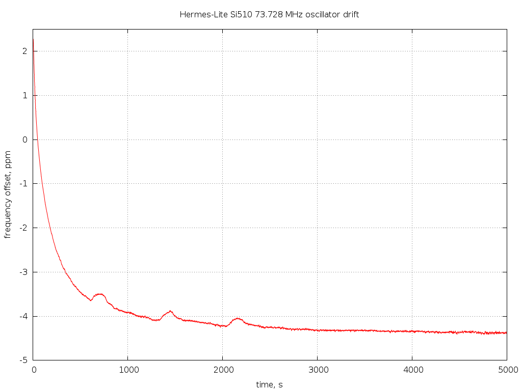
The drift during TX is just about 0.2 ppm, which seems not too bad but translates actually to 2 Hz at 10 MHz and this may be objectionable for WSPR, where a drift below 1 Hz during the transmit period is usually recommended.
The measured frequency over time data used for the graph above can be downloaded here (gzip compressed). Note that the frequency points are not uniformly sampled due to some peculiarities of the counter used.