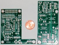
K2DI v.III and K2DI-PCI PC Boards

K2DI v.III and K2DI-PCI PC Boards
OVERVIEW
As mentioned in the NEW IDEAS, NEW SET-UP paragraph on my DI v.II.2 Technical Info and Schematics page, and following my way of thought to get a suitable K2 external connection for digital modes, on November 2003 I developed a set of two Printed Circuit Boards, namely the K2DI v.III and the K2DI-PCI.
These two boards have been designed to be intalled in the basic QRP K2 and are compatible with the KAF2 or KDSP2 and KBT2 options. Because of this feature, they are also good for the split K2-KPA100+KAT100 set-up.
The solution of an external digital connection for the integrated K2/100, using the DI v.II.2, is widely discussed in the K2/100 page.
CHARACTERISTICS
The set's main board, or motherboard, is the K2DI v.III, which uses the very same circuitry as its predecessor v.II.2. It only differs in its layout that has rendered a smaller board, which still offers all the v.II.2 features, i.e.: a Mike Configuration Header Extender and connectivity to a Rear Panel Data Connector, as well as a buffered, fixed audio output and the cutting of the Front Panel microphone connector's AF and PTT lines, when transmitting data, so that no unwanted sound (shack's noise) may be transmitted by a life mic. No need to unplug your microphone. A very handy feature when working SSTV.
K2DI-PCI is an optional complementary daughterboard, which may be assembled to the K2DI to conform a complete Computer's Interface for the Basic K2 or the split K2/100. This board features direct connectivity to the computer's sound card LineIn/LineOut connectors, duly isolated by a couple of 600:600 transformers. The output AF signal level is set by means of a 10K pot. It also features a selectable Tone or RS232 PTT switch to meet the user's needs and/or preferences. Selection is made using a couple of jumpers and the RS232 option is isolated by means of an optocoupler.
The next table of text and images will help understanding my explanation.
Clicking on any and all of the thumbnails a new window will be opened to display an enlarged picture of the chosen snapshot. To close that new window just click on the image displayed.
K2DI v.III Board, Digital Interface
K2DI-PCI Board, Computer Interface
K2DI-PCI Board, Computer Interface, assembled to the
K2DI v.III, Digital Interface
COMMENTS
I wish to remark the fact that these two boards are complementary and because of that, in some way, they can be used separately.
The K2DI v.III is the motherboard, the Basic K2 Digital Interface that brings out digital signals to one rear digital connector from where, with the help of an external Computer Interface, feed them to a computer to work digital modes.
The K2DI-PCI, featuring LineIn LineOut isolation and selectable Serial(RS232)/Tone PTT switch, is an optional board and as such it can be used in two ways:
a.- As daughterboard to the K2DI v.III Digital Interface to conform a complete Digital-Computer Interface, that will only need the right cable to link it directly to the computer (no need of an external computer interface) to make the Basic K2 ready for digital operation. It is my thought that it may be ideal for backpackers.
b.- As a stand alone external Computer Interface for the K2, K2/100 or any other brand of transceiver featuring Digital modes connectivity. In this case the user will have to work on the construction of the right enclosure for such an interface and its characteristics to meet his or her needs. Selectable multi rig connection?
Please visit the Basic K2 - Split K2/100 Set-up for further details on the installation of these two boards or download the Construction Manual available as a .PDF file at the Downloads page.
 CAUTION:
If and when using the VOX (Tone) PTT option, care must be taken to mute, at your OS, all the sounds and chimes scheduled to announce Windows and other programs events or happenings (Start -> Configuration -> Control Panel -> Sound, Audio and Voice Devices -> Change Sound Scheme -> Properties -> Sound). It is most important that no unwanted sound is produced. Otherwise, those sounds will inadvertently trigger the PTT and, to our own despair and annoyance or what is more embarrassing, to that of the contacted remote station or the listeners, the unwanted sound will be transmitted.
If your Sound Card has the full duplex feature, when setting the Sound Card Mixer, remember to mute the Line In or Microphone In at the Sound Level Control, so that the received audio or noise is not echoed to the Line Out outlet and thus get the PTT switched On continuously.
AVAILABILITY
I have a small stock of PCBs. If you are interested in my project please do not doubt to contact me. Thank you.
Modified on April 2, 2004.