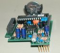
This image shows the modified KAF2 P2 3-pin male header. I substituted 2 of the standard pins (#1 and #2) of the P2 3-pin male header for 2 longer ones so that when the header was soldered, I had the normal 3 male pins on the bottom side of the KAF2 board to be plugged to J2 at the control board and 2 male pins on the top face of the board to connect a cable to feed the AF signal to J4 at the K2DI v.III.

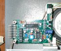
Here we have a modified KDSP2 P2 3-pin male header. As I did with the KAF2, I substituted 2 of the standard pins (#1 and #2) of the P2 3-pin male header for 2 longer ones so that when the header was soldered, I had the normal 3 male pins on the bottom side of the KDSP2 board to be plugged to J2 at the control board and 2 male pins on the top face of the board to connect a cable to feed the AF signal to J4 at the K2DI v.III.

Side view of the installed K2DI v.III Digital Interface. This board is prepared to receive its daughterboard, the K2DI-PCI. That's why we have three stand-off installed, the electrolytic capacitors are low profile and C5, the 220uF capacitor, is bended. .

The installed K2DI v.III Digital Interface as seen from above.

This picture shows the bottom side of the K2 upper cover, with all the options, i.e. KAT2, KIO2 and KBT2, installed and coexisting with the K2DI v.III Digital Interface.

Side view of the Digital-Computer Interface, i.e. the assembled K2DI V.III and the K2DI-PCI boards.

Top view of the complete Digital-Computer Interface already installed and ready for use.

Rear view of my Basic K2 showing my Digital connectors setup. You will notice I have taken advantage of the holes formerly provided for the connection of Elecraft's transverters to install a 4 pin MiniDIN connector on the IN XVTR hole, for the soundcard connection, and an isolated Minijack stereo connector on the OUT XVTR hole for the Serial PTT connection.

Top view showing how I have fixed the K2DI-PCI cables on the top cover of the Basic K2. You will notice I have removed the K2BAT.
This side view of my Basic K2 shows how I have installed a Minijack stereo for the Serial PTT rear connection. Notice the bakelite washer used to isolate the PC signal GND from the K2's chassis.
