IZ1PMX VECTORIAL NETWORK ANALYZER |
If an "miniVNA" is too expensive or if you like to build an useful RF instrument, IZ1PMX vectorial network analyser will be a good choice.
Thank you Alfredo for help and for your ham spirit!
Features of IZ1PMX VNA:
Recommanded upper limit of frequency: 180MHz (AD9951, 500MHz clock).
Maximum frequency: 250MHz
Dynamical range in detection mode: 70dB (AD8307)
Return loss of directional coupler: -25dB...-34dB.
LCD Display: 88x44 (Nokia 5110,3310) or 128x64 (ST7920)
PC connection: RS232, USB FT232 or Bluetooth HC-06.
PC Software supported: IZ1PMX - IT_VNA; VNAJ; IG miniVNA
IZ1PMX VNA is capable to use two DDS chips: AD9850 (50MHz) or AD9951 (180MHz). Bellow i will speak only about AD9951 version.
For more details: Link to IZ1PMX web site.
The DDS oscillator is capable to generate signals up to 250MHz. Internal PLL multiplier (x20) is used for 500MHz clocking, using 25MHz external crystal. Software calibration of the output frequency is done at 30MHz. My VNA was limited to 180MHz by using a Cauer LPF 180MHz/-3dB. At the begin, LPF is possible to be bypassed. LPF must to be recalculated if maximum frequency >180MHz. The coils of filter can be hand made when SMD coils are not available.
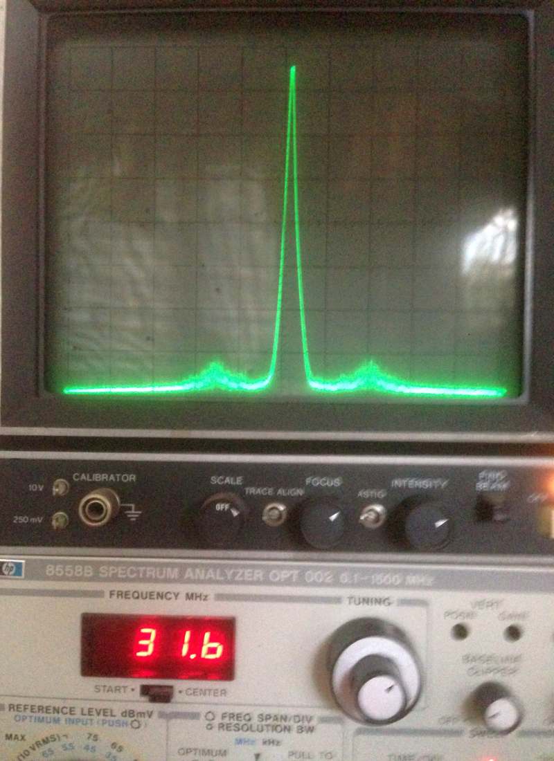
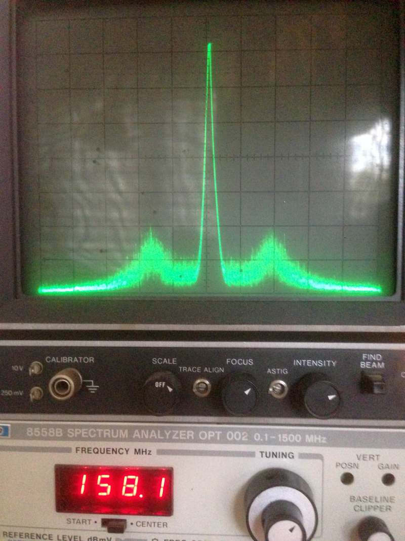
Phase noise performances of the DDS are not very good due usage of internal PLL multiplier (like miniVNA). Here is possible to see my spectrum analyzer connected at VNA output: ~ 30MHz and 160MHz.
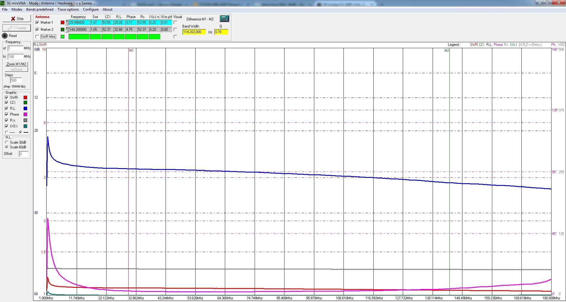
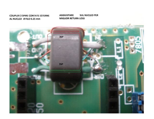
The directional coupler is compensated with a small capacitor, in order to increase the return loss (RL). This capacitor will be adjusted for best RL and flat response between 0-180MHz. Connect a good quality -20dB attenuator between DUT and DET. Adjust the capacitor and directional coupling turns for best RL/phase response. Position of turns inside of directional coupler can improve the RL. After calibration, the turns must to be secured. Tipical response during RL adjustement.
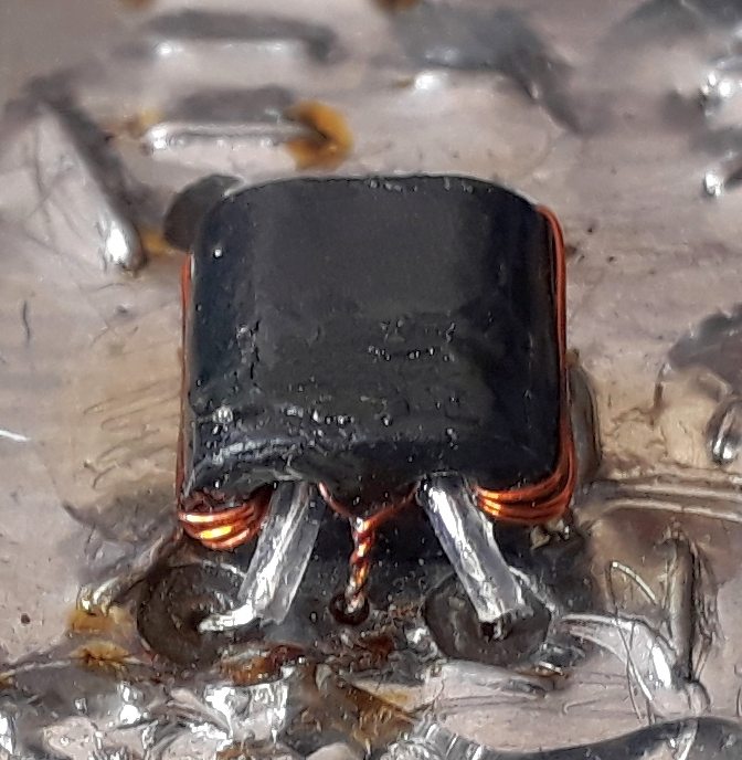
Binocular ferrites BN43-2402 were used for directional coupler and DDS balun. I experimented with some ferrite types, but BN43-2404 remain a good choice regarding frequency bandwidth and RL. Frequency response is poor under 2MHz. Also insertion loss increase after 160MHz, valid measurements are possible up to 180MHz. Mini-Circuits PDC-10 directional coupler can replace the home made coupler.
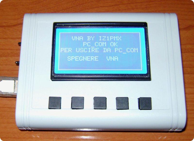
Data connection for PC can be RS232 or USB. ADM232 convert serial TTL levels to RS232. I like to use this IC because it required 100nF capacitors for voltage convertors. Is possible to be replaced with MAX232, check datasheet for more details. I recommend to use an external USB-serial convertor, like as FT232. Do not use PL2303, many problems under Windows 7 (for XP is ok). Cordless connection by Bluetooth is a another possibility. Take care, VNA inputs can be perturbed by Bluetooth radio signal. USB and Bluetooth interfaces (HC-06) are frequently used in Arduino projects. PC communication is active when pin 15 of uC is connected to ground (i don't use). Is enough to enable PC mode from VNA menu. Select "PC_PMX mode" for IZ1PMX software or "PC_VNAJ mode" for IGminiVNA or VNAJ PC software.
The LCD is necessary for calibrations, PC software selection and diagrams. Usually, IZ1PMX firmwares are designed for 128x64 - ST7920 controller. For LCD 88x44 is necessary a dedicated firmware. This kind of LCD was found in Nokia 5110 or 3310 series. Pinouts are not identically!
The resistiv network for keyboard is supplied with 1,8V from a small voltage regulator. IZ1PMX use AD8302 REFOUT to supply the keyboard resistors. Analogic and digital voltages for AD9951 are supplied by different regulators.
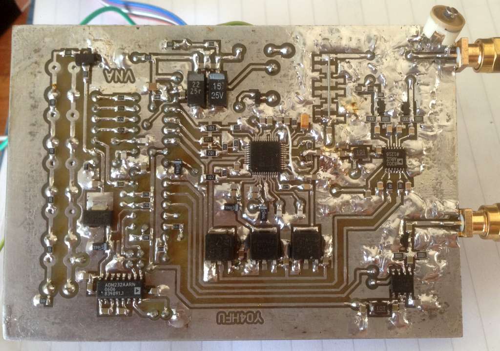
My VNA use a single PCB, AD9951 is placed on same board. IZ1PMX kits have some connectors between VNA pcb and DDS board.
I like to use wrap wires for connections on top side, to preserve the ground plane. Gicu - YO8RLK made slightly modifications on top side of the PCB, few traces were created. Both PCBs are available to download.
Two SMA connectors offer external connection for Transmission (DET) and Reflection (DUT) ports. Microstrip lines were calculated for 2,5mm FR4 pcb. SMA connectors can be replaced with good quality BNC connectors.
"Detector port" - uWattmeter function. Because AD8307 is used also for normal VNA Transmisson mode, i modified the schematic. Two variable resistors and one switch are used for separate calibration. In this way, uWattmeter function remain accurate.
LPF 180MHz hand made coils: 39nH=4 turns; 56nH=5 turns; 68nH=6 turns. Wire 0,5mm, internal diameter 2,5mm, air wound, no distance between turns.
Update 01.2017
During VNA usage with IGminiVNA software, inaccurate measurements were observed in Transmission Mode. Transmission Loss "dB" indication is wrong. The malfunction can be fixed with different calibration value, "790" value required by uC VNA software must to be "870" for IGminiVNA PC software.
Here is possible to find my modification. After that, insertion loss has good accuracy between 0...-50dB. Before any measurement, do not forget to calibrate IGminiVNA (Configure>miniVNA>Calibrate Transmission).
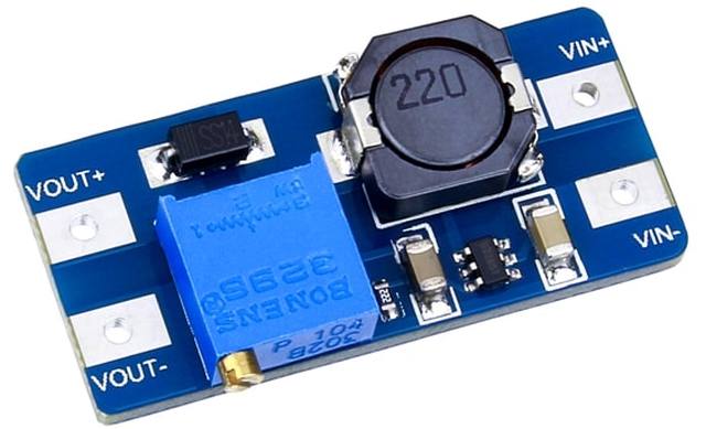
VNA power supply using LiPo battery and a step-up DC/DC converter MT3608 adjusted for 7V output. The battery is charged from USB port using TP4056 Board at 450mA, 2K7 resistor).
3,7V/1Ah battery has 60 minutes autonomy.
![]()
SCHEMATICS:
Block Diagram
IZ1PMX VNA - Schematic rev.1.1 - 04.2021 (LCD pinout fixed)
AD8307 detector - uWattmeter modification
88x44 Nokia Display pinouts - link
128x64 LCD ST7920 controller - jumper settings
Directional coupler: >1< , >2<
PCB:
PCB vers.1 (yo4hfu) - pdf + Sprint Layout 5.0 file
PCB vers. 2 (yo8rlk) - only Sprint Layout 6.0 file
FIRMWARE ATmega328:
Vers. 1.6 for 128x64 LCD
Vers. 1.6 for 128x64 LCD - Romanian Language
Vers. 1.8 for 128x64 LCD - slowly response...
Firmware for 88x44 LCD
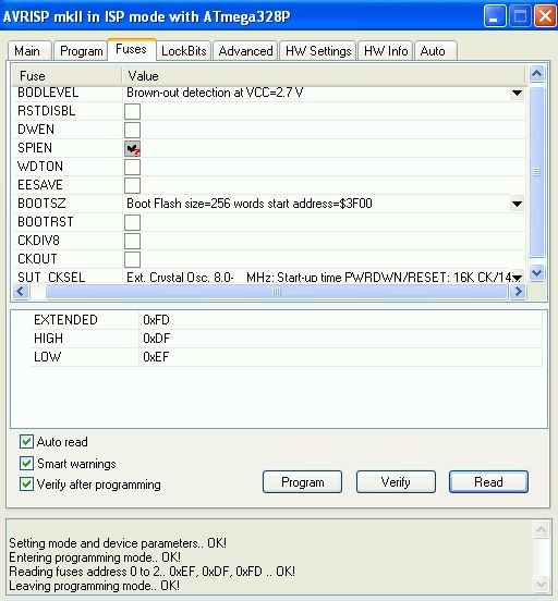
Fuse bits configuration of ATmega328 uC
PC SOFTWARE:
PC Software IT_VNA (iz1pmx) - link
PC Software VNAJ - link
PC Software IG miniVNA (easy to use) - link
FT232L UART Driver - link
YO4HFU PHOTOS:
Bottom side pcb
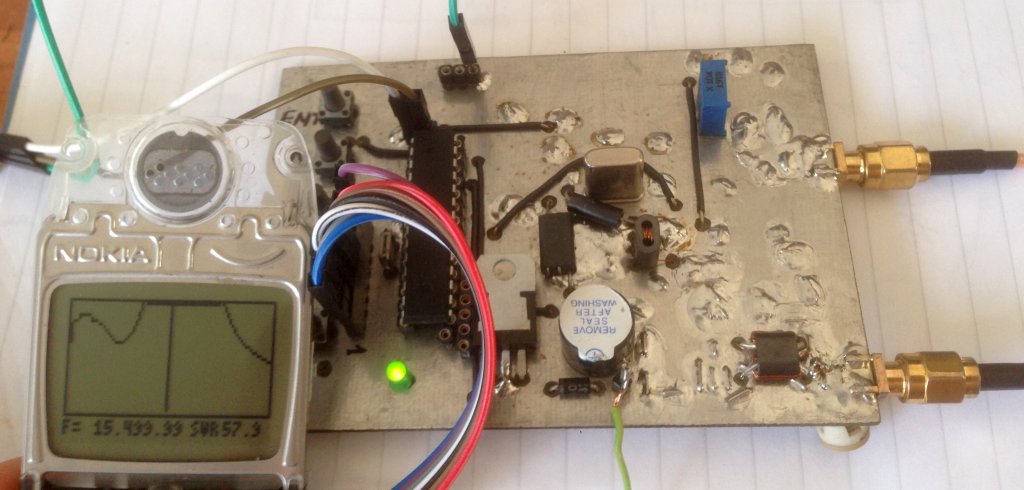
Nokia display
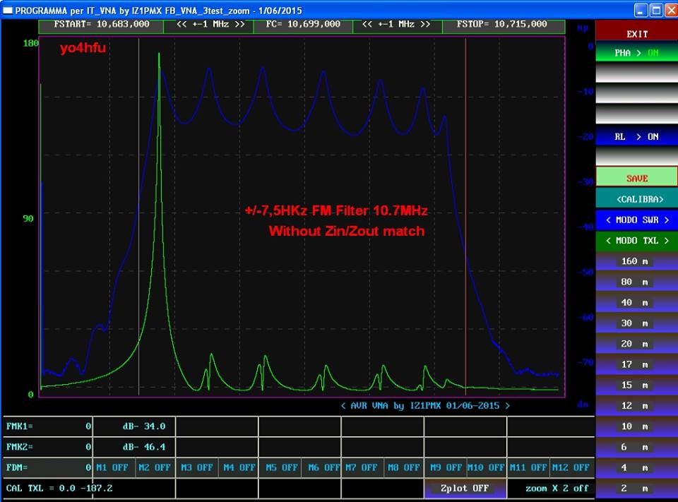
10,7MHz FM Filter Demo
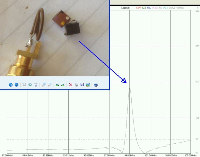
VNA grid-dipmeter