SI5351A QUARTZ REPLACEMENT OSCILLATOR |
The Si5351 clock generator offers a simplified design, making it an ideal solution for a wide range of applications.
Key Features:
-
Wide Output Frequency Range: Capable of generating frequencies from below 8 kHz up to over 200 MHz ( 3.6KHz...292MHz)
-
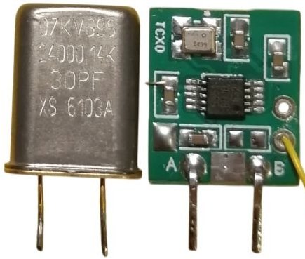
Compact Design: Small PCB footprint compatible with HC-49U crystals, ideal for replacing exotic or hard-to-find quartz resonators.
-
High Stability Oscillator: Equipped with a high-stability TCXO (0.5 ppm) of 25 MHz or 27 MHz (10...100MHz)
-
Dual Frequency Support: Ability to generate real-time switchable frequencies, e.g., BFO USB/LSB.
-
Arduino IDE Compatibility: Utilizes an affordable Attiny25/45/85 MCU, programmable via the Arduino IDE.
The SI5351 clock generator is renowned for its excellent performance, cost-effectiveness, and versatility. In this project, the design has been significantly simplified compared to earlier implementations that relied on the ATMEGA328 MCU and complex libraries.
By opting for an Attiny MCU and a light library, memory usage has been minimized without compromising functionality.
The PCB layout is compatible with HC-49U crystal footprints, making it a practical replacement for quartz resonators, particularly in applications requiring uncommon frequencies. A 0.5 ppm miniature TCXO replaces the traditional 25/27 MHz crystal reference oscillator. Although this configuration deviates from SI5351 datasheet recommendations, the TCXO is directly connected to Pin 2 XA, yielding excellent results. I did some measurements and minimum clock level is around -16dBm. Upper limit can accept even +13dBm. Avoid more than 3Vpp input! As external reference I prefer 0...+5dBm.
As the TCXO, the EPSON TG2520SMN 27.0000M-MCGNNM3 (0.5 ppm, available from Mouser) was selected, but other models with a 3.3V supply and dimensions of 3.2x2.5 mm, 2.5x2 mm, or 2x1.6 mm can also be used.
Key Functionalities:
Pin 3 of the MCU can toggle between two user-defined frequencies configured in the firmware.
-
Sketch development is based on QRP-Labs' implementation, further adapted by LZ2WSG for Attiny compatibility, and additional enhancements from my side.
-
Power consumption is optimized by disabling unused outputs, achieving a minimal draw of approximately 25 mA at 5V (typical 18mA).
![]() Programming and Usage:
Programming and Usage:
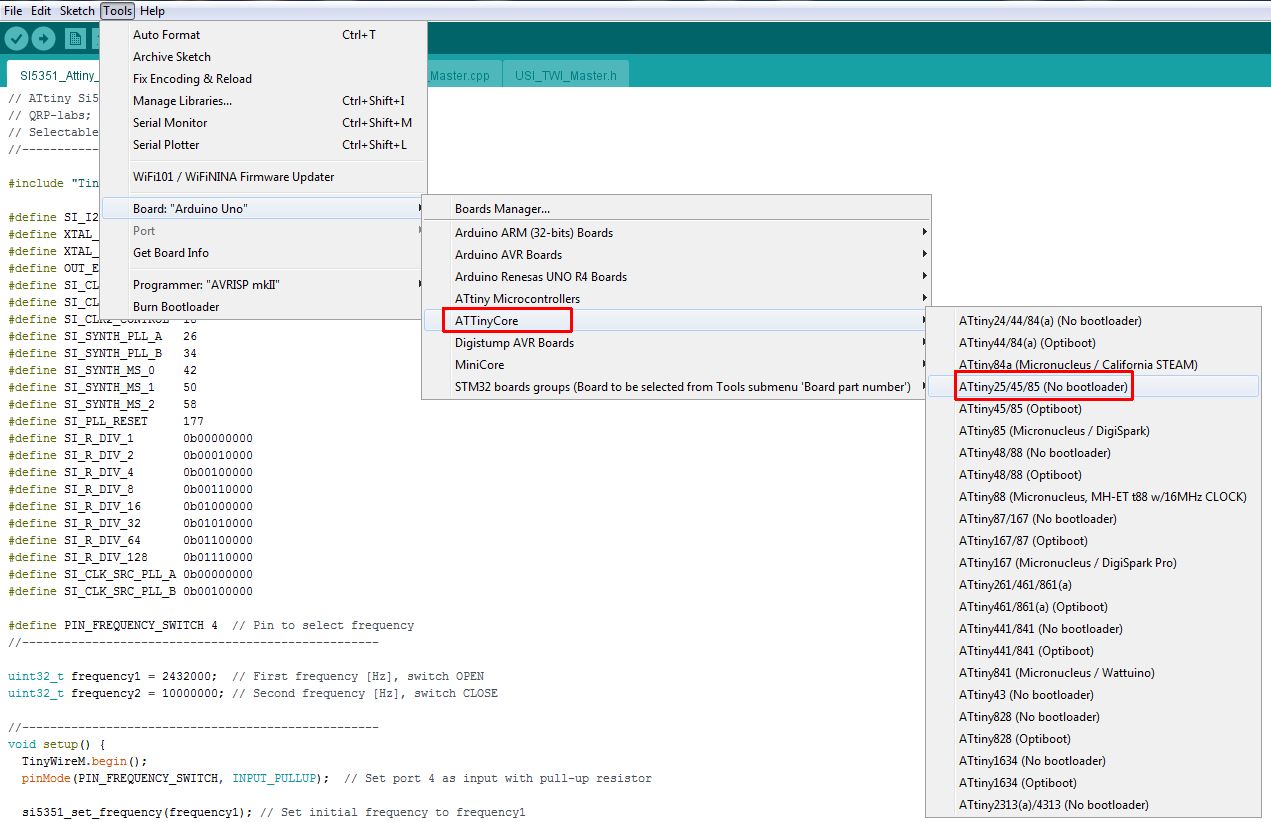
To configure the device, open the provided sketch file (.ino) in the Arduino IDE. Modify the two preset frequencies as required, then compile the code to generate the corresponding hex file ( Sketch > Export Compiled Binary ). Ensure that the AttinyCore library is installed in the Arduino IDE for full support. It is preferable that the MCU be programmed before installing the SI5351 to avoid any conflict during writing.
The firmware is compact enough to fit even on the smallest Attiny25 MCU, with default fuse bits set for 1 MHz internal clock. Note that the Attiny package SOIC-8 package (4 mm wide) and SOIC-8 Wide (8S2 / 5.4 mm) can be installed.
Attention to the I2C address of the SI5351; it needs to be defined within the program. Usually, it is 0x60, but in my case, it had to be changed to 0x62 (SI5351A purchased from Farnell few years ago).
Note: recommended supply voltage 5V, maximum 6V! (TPS79333 specs).
![]()
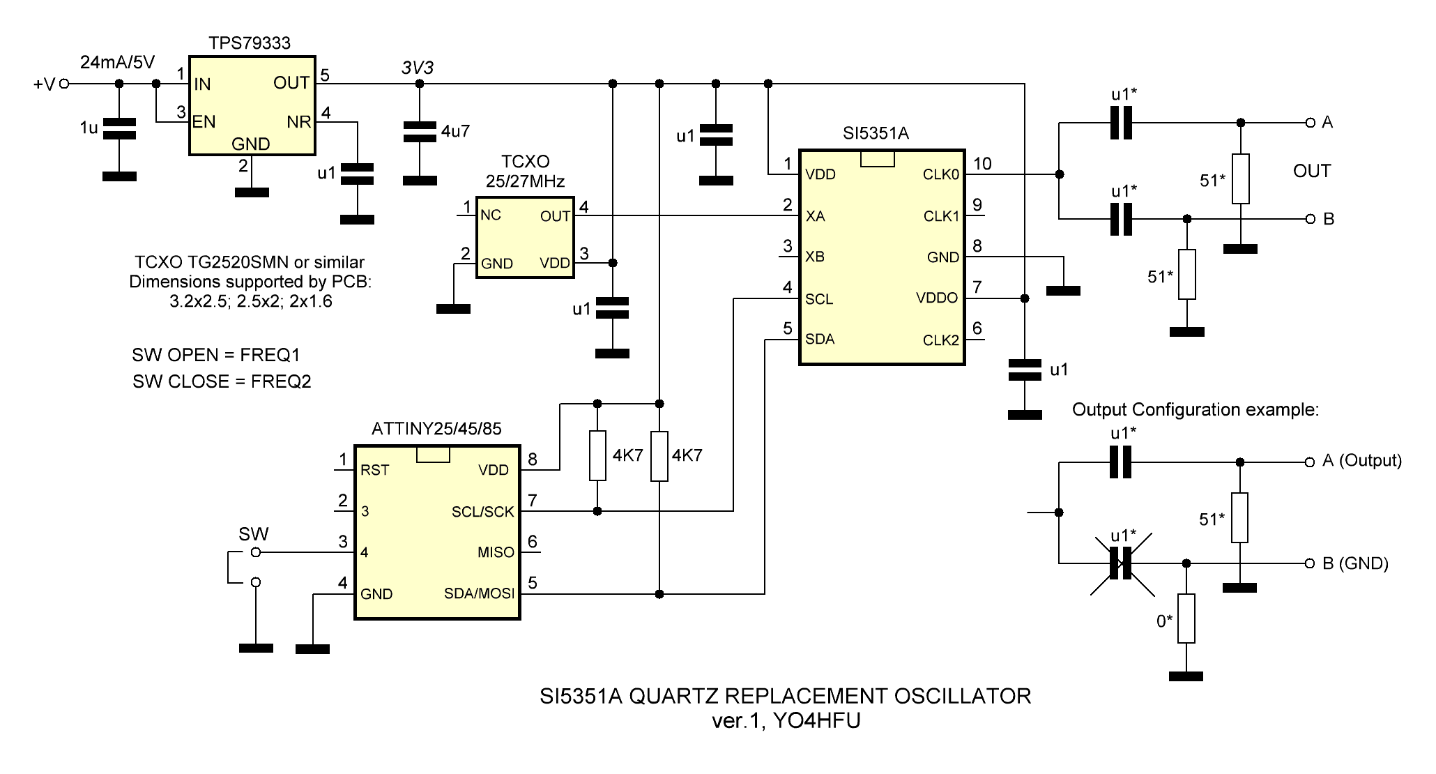
![]() SI5351A & ATtiny schematic
SI5351A & ATtiny schematic
![]() PCB v1.1 (Gerber)
PCB v1.1 (Gerber)
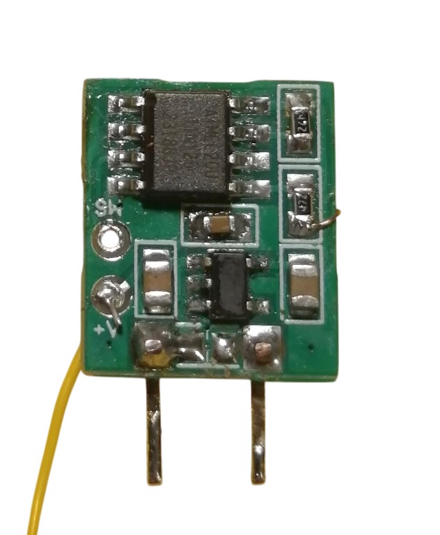
![]() PCB top view
PCB top view
![]() PCB bottom view
PCB bottom view
![]()
![]() SI5351A & ATtiny switch frequency sketch v1
SI5351A & ATtiny switch frequency sketch v1
![]() SI5351A & ATtiny fixed frequency sketch v1 (no switch, only one fixed frequency)
SI5351A & ATtiny fixed frequency sketch v1 (no switch, only one fixed frequency)
![]() >> Link to ATTinyCore 2.0 <<
>> Link to ATTinyCore 2.0 <<
![]() ATTinyCore selection
ATTinyCore selection
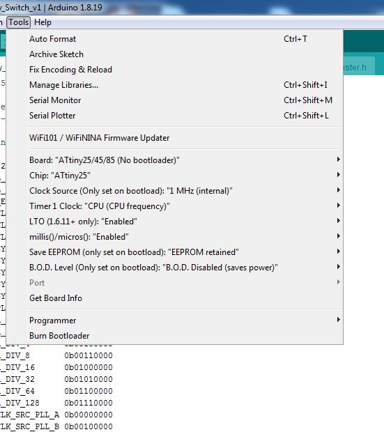
![]() ATTinyCore configuration
ATTinyCore configuration
![]()
![]() Firmware HEX - 1.216MHz, no switch, 0x60 (useful for stereo coder - David III)
Firmware HEX - 1.216MHz, no switch, 0x60 (useful for stereo coder - David III)
![]() Firmware HEX - 1.216MHz, no switch, 0x62
Firmware HEX - 1.216MHz, no switch, 0x62
![]() Firmware HEX - 2.432MHz, no switch, 0x60 (useful for stereo coder DB)
Firmware HEX - 2.432MHz, no switch, 0x60 (useful for stereo coder DB)
![]() Firmware HEX - 2.432MHz, no switch, 0x62
Firmware HEX - 2.432MHz, no switch, 0x62