During last periode of time, parts from scrapped Wavelab ODU SP+ are available on Ebay. Most common ODUs are designed for 18GHz, 23GHz, 38GHz.
23GHz item has been studied in detail by our Polish colleagues. Wavelab topic can be found on Mikrofale.Cafe forum.
RF unit can be easily reused to 24GHz with excellent results (2W maximum output).
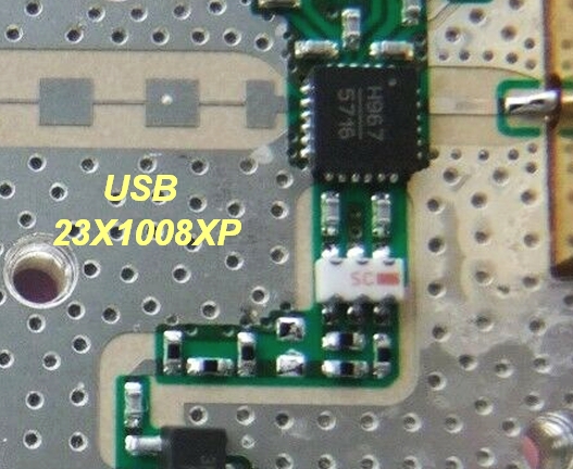
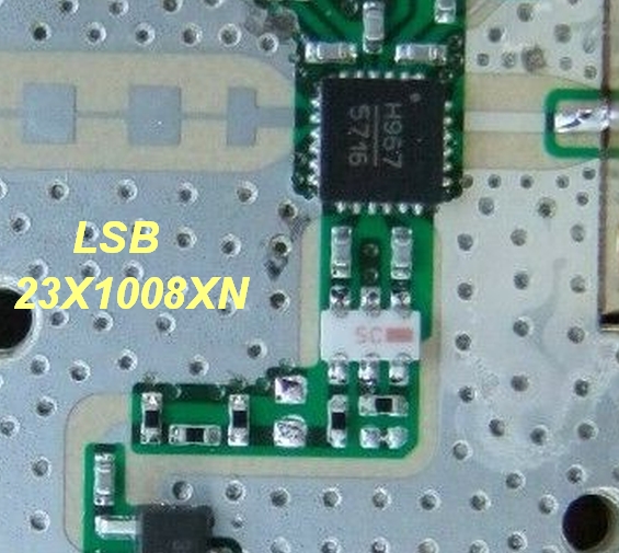
![]() Two different RF units can be found:
Two different RF units can be found:
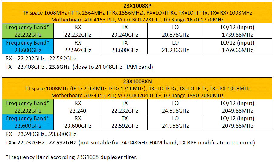
- 23X1008XP; band 23GHz; TR spacing 1008MHz; RX frequency lower than TX.
- 23X1008XN; band 23GHz; TR spacing 1008MHz; RX frequency higher than TX.
According Wavelab ODU brochure, frequency range is 21.2-23.6GHz but original PCB LO can't reach 21.2GHz. Duplexer filter marking: High Band port 23240-23600MHz and Low Band port 22232-22592MHz.
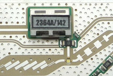
TX IF is 2364MHz/BW~140MHz, ceramic BPF located inside of microwave module.
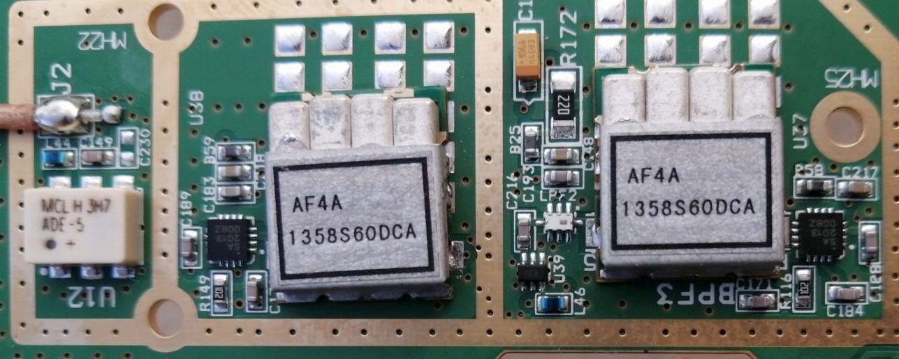
RX IF is 1356MHz/BW~60MHz, 1358MHz ceramic filters located on the montherboard. We suppose RX IF 1356MHz and not 1358MHz, in order to solve 1008MHz duplex shift (2364-1356=1008)
XP RX front end is configured to select USB (RF-LO). XN RX front end is configured to select LSB (LO-RF), IF spectrum is mirrored.
TX sub-harmonic mixer is same for both units, but selected single side band is different, appropiate TX BPF is used.
![]() Conversion to 24.048GHz HAM band:
Conversion to 24.048GHz HAM band:
No internal modification are required for 23X100XP, TX output power is up to 2W.
Very low TX output @ 24.048GHz was observed for 23X1008XN. Frequency response of internal TX bandpass filter needs to be increased by hardware modification.
One more problem is the band plan of LO chain, this leads to restrictions regarding optimal 1st IF. LO outside of designed bandpass range may affect RX gain.
RX front end is wideband, no band pass filter, so NF is expected to be almost same at 24GHz (low gain can affect the global NF, gain compensation on RX IF will be required).
Possible LO range according measurement of internal filters:
XP input LO 1580...1850MHz. First stage [x2] multipler can be "forced" by using 790...925MHz [x3] or 3160...3700MHz [x1].
XN input LO 1883...2166MHz. First stage [x2] multipler can be "forced" by using 941.5...1083MHz [x3] or 3766...4332MHz [x1].
I did some measurements and the best result is to use the LO range according factory design.
Best result for XP version is obtained using LO 1808MHz/ ~0dBm and RX/TX IF 2352MHz, enough RX gain and clean TX output. Good results are obtained also using 3616MHz.
Input LO level is not critical, that means the LO chain working properly. Maximum required TX IF level is 5dBm for 24GHz saturated output.
Similar RX gain is maintained between 2100-2600MHz IF. Do not use RX IF less than 2100MHz, the gain will be affected due to low LO level (LO chain outside of designed pass band).
Poor result was observed in case of LO 904MHz, the level is critical and is not same for RX and TX. RX gain is less than normal and TX output has spurious (monitoring voltage seems to be normal but the 24GHz carrier is low).
I prefer LO1 3616MHz in order to avoid MAX2871 /2 divider of internal VCO and then x2 multiplication inside of Wavelab.
![]() For more details read about new IF Converter / Controller for Wavelab ODU project.
For more details read about new IF Converter / Controller for Wavelab ODU project.
Other observations:
![]() TX monitoring detector voltage is negative, -3.2V @ saturated output power. Inverting OA will be necessary in front of uC ADC port. OA supply +/-5V. (LE: One RF unit with -1.5V monitoring voltage was found, probably different diode)
TX monitoring detector voltage is negative, -3.2V @ saturated output power. Inverting OA will be necessary in front of uC ADC port. OA supply +/-5V. (LE: One RF unit with -1.5V monitoring voltage was found, probably different diode)
![]() Internal temperature sensor is not a termistor as I first thought, it is a diode. It was used as reference for TX output monitoring amplifier. I intend to use it as internal temperature sensor (-1.2mV/C).
Internal temperature sensor is not a termistor as I first thought, it is a diode. It was used as reference for TX output monitoring amplifier. I intend to use it as internal temperature sensor (-1.2mV/C).
![]() ATT1 & ATT2 terminals can be left floating or grounded for maximum TX power (minimum PIN attenuation). Output power can be controled by 2KΩ potentiometer between +5V and ATT2.
ATT1 & ATT2 terminals can be left floating or grounded for maximum TX power (minimum PIN attenuation). Output power can be controled by 2KΩ potentiometer between +5V and ATT2.
Of course, if attenuation is used, maximum output power will be obtained by increasing TX IF level and compression will occur.
![]() +5V RX can be connected to common +5V RX/TX if absorbed current is not important.
+5V RX can be connected to common +5V RX/TX if absorbed current is not important.
Note:
The initial measurement and pinout identification was made by Paweł SQ1GQC and Staszek SP6GWB.
LO chain pass band & locking range of XN/XP PLL LO boards was measured by Andrzej SP8XXN.
I/O PCB adapter BOM: screws M2.5x12; 0.45mm (6 pcs) and 1.27mm header 20 pins 20021111-00020T4LF Amphenol (3 pcs)
![]()
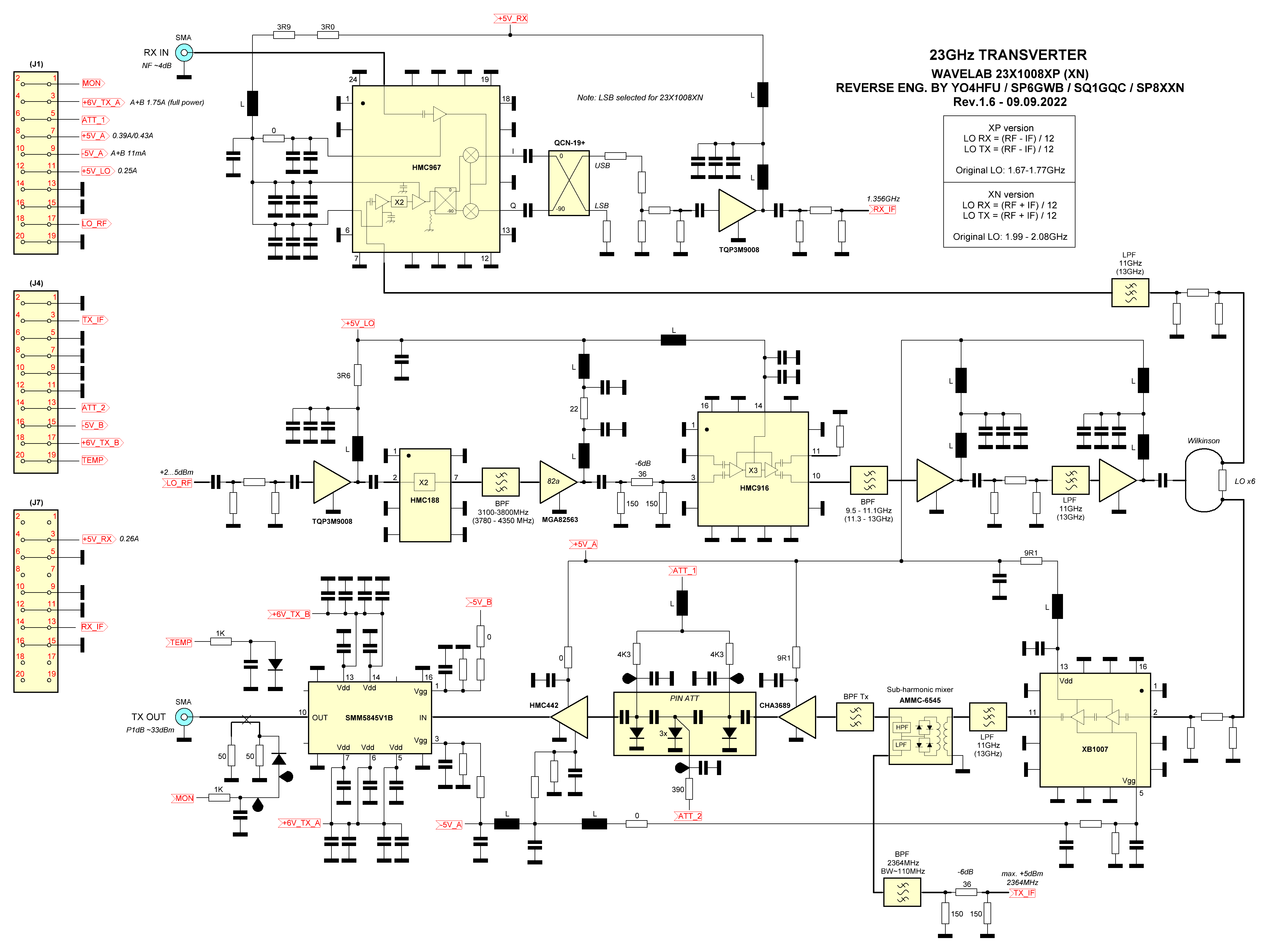
![]() WAVELAB 23X1008XP/XN schematic rev.1.6 (reverse engineering)
WAVELAB 23X1008XP/XN schematic rev.1.6 (reverse engineering)
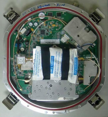
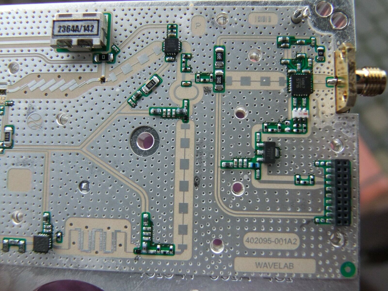
![]() Internal view of Wavelab 23GHz XP part 1
Internal view of Wavelab 23GHz XP part 1
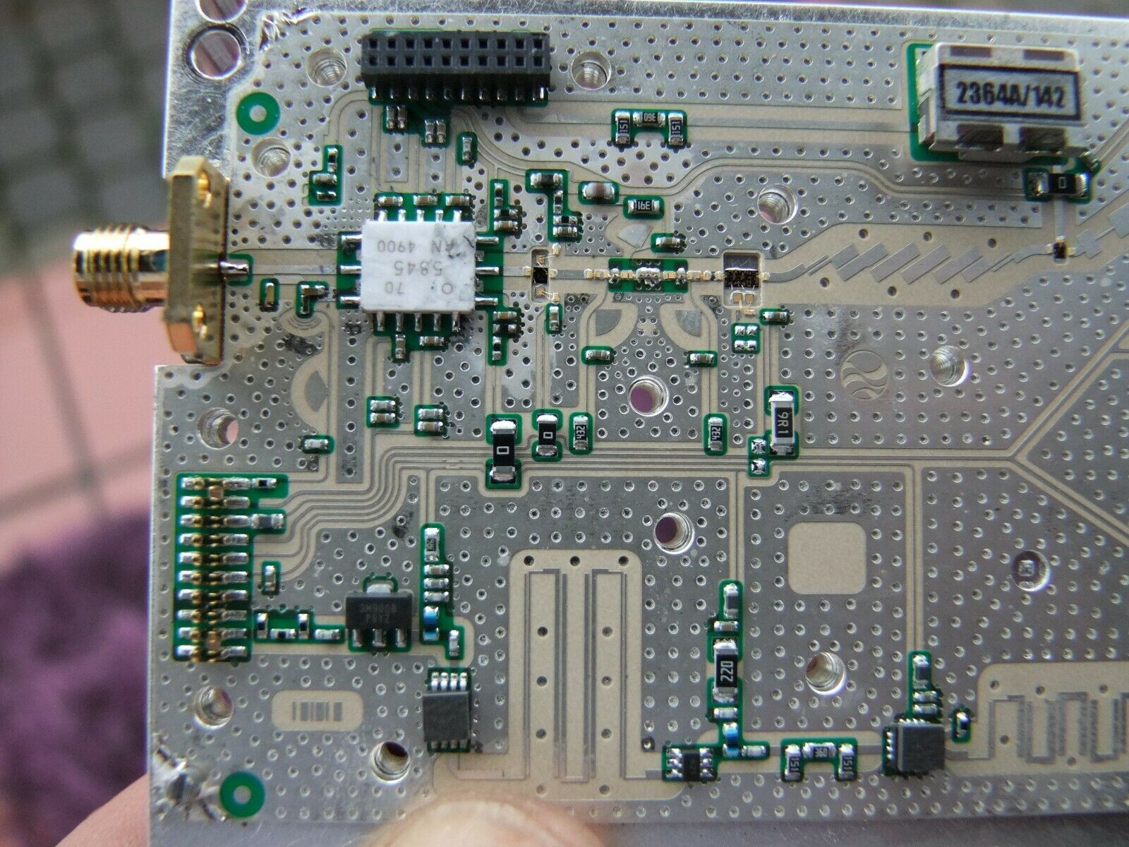
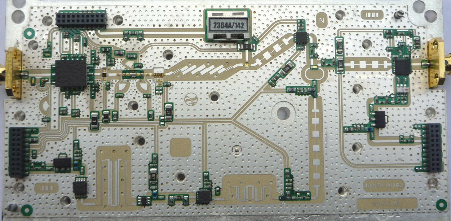
![]() Internal view of Wavelab 23GHz XP part 2
Internal view of Wavelab 23GHz XP part 2
![]() Internal view of Wavelab 23GHz XN
Internal view of Wavelab 23GHz XN
![]() I/O PCB adapter SQ1GQC (gerber files - link)
I/O PCB adapter SQ1GQC (gerber files - link)
![]() HB9AFO website
HB9AFO website
![]() NTMS PA0HME Wavelab and NTMS Optimisation part 1 - unfortunately, the author doesn't specify the source of documentation...
NTMS PA0HME Wavelab and NTMS Optimisation part 1 - unfortunately, the author doesn't specify the source of documentation...
yo4hfu@2010-2026