Receiver Modifications || || 1496 IC Mixer Front End
Driver || Final Amplifier || Lowpass Filters || Antenna Switching
|
The following are my initial efforts at putting together a transmitter to work in transceive mode with the Electroluminescent Receiver Kit. Using a stabilizer with the receiver VFO, the transmit stability has been excellent and the circuit used for keying has been given lots of compliments. The final schematics and my dead bug pictures of the transmitter will be shown: First, modifications to the ELR - adding two relays, second, the front end of the transmitter - mixer, oscillator, keying, and mute circuits. The mixer output goes to the receiver RF Amplifier and Bandpass filters to amplify and clean the broadband output of the mixer. Third, schematics and pictures for the RF driver, amplifier, and lowpass filters. The picture below is a block diagram of the transmitter and interface with the receiver. |
|
Two SPDT relays are glued to each end of Section 2 as shown in the above picture. Wires for the coil ground (and cable grounds) can also be used to hold the relays down (as shown in the pictures below) soldered to the ground plane below the line of holes between Section 2 and 3. The trace between the INPUT OUT and INPUT IN is cut to allow the lower relay to switch the output of the Bandpass Filters. Antenna Relay |
|
The cable from the Antenna relay goes to the output of the 1496 IC in the transmitter. Section 2 provides amplification (RF Amplifier) and Filtering (Bandpass Filters) for the output of the 1496 mixer. Since the receiver is tuned for the band being used, it is automatically ready to properly filter the output of the mixer. The result is a very clean output of the mixer amplified just the right amount for the first transmitter RF amplifier. Notice the 1N914 diode between the coil connections on the relay with the band going to the 12 connection of the relay (top one in the picture above). Bandpass Filter Relay |
|
The bottom copper trace between the INPUT OUT and INPUT IN is cut to allow the lower relay to switch the output of the Bandpass Filters. The cable of the Bandpass relay goes to the first transmitter RF amplifier input which drives the Final Amplifier. Notice the .01 bypass capacitor between the coil leads. The 12 Volt connections of the relays are connected. A wire from the 12 connections goes to the transmitter switching circuit that controls these relays, muting, and antenna relay switch. |
|
A third IRED allows IR switching of the transmitter lowpass filters with the switching of the receiver's bandpass filters. The IREDs are connected in series. The relay's coil resistance provides protection and voltage for the IREDs and are grounded by the IRED above the right hand side of the 20/17 relay. The Commercial blue emitter shown above is used in this build. If you are mounting the transmitter separate from the receiver, this commercial pair of emitter/receiver and optical cable can to used to automatically switch the lowpass filters of the transmitter. If the transmitter is stacked above the receiver, a hole is drilled Board 2 above the IRED to line up with a phototransistor (that points down from a hole in the lowpass section of the transmitter) that switches the lowpass filters in the transmitter. Pictures of this later. Another solution is to separately switch the lowpass filters in the transmitter and not use any fiber optics or IR light. Commercial Pairs w/1000µm Optical Fiber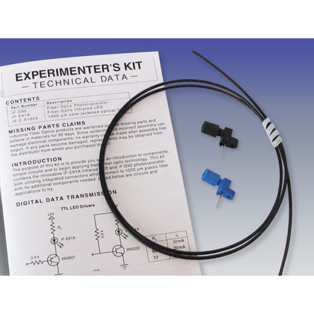 Blue - IRED Emitter || Black - Phototransistor Receiver This pair of emitter/receiver and optic fiber is called the Experimenter's Kit IF-E10 in the Fiber Optics Kit section of Circuit Specialists web site. It contains a matched pair emitter/detector as pictured above and 1 meter of 1000µm optical fiber. |
|
1. Short C & E on the Crystal Oscillator Phototransistor - BPX-38. This is to lock the Crystal Oscillator to the 3.457 MHz crystal. 2. Remove the black tubing between the Crystal Filter and the phototransistor at the Crystal Oscillator. 4. Change the 3.547 MHz Crystal Filter to 4.000 MHz crystals - total of three. VFO Modifications for a Single 4MHz IF Frequency5. Change the 68pf cap at the 10.545 relay to 47pf, then move the 40 meter VFO to 11.000 MHz. 6. Parallel an 82pf cap to the 35pf trimmer next to the 10.455 relay (underneath the board), and then move the 20 meter VFO to 10.000MHz. |
|
The above schematics have been built and used on the air.
This circuit resolves the problem with chirp in the 4 MHz oscillator with the differential circuit turning on the oscillator before the active mixer. A diode mixer can not be turned off, but an active mixer can, in this case a 1496. The mute for the receiver, antenna switch, and the Bandpass Filter relays are keyed the same time as the oscillator, then the mixer is turned on. Keying is excellent and clean. The 1496 uses low level signals so the VFO output, from a 3.3pf cap from between the two VFO amplifiers on the receiver board, to the connecting coax, provides the correct drive level for the 1496. The output of the 1496 mixer labeled "To Filters" goes to the Antenna relay on Section 2 of Board 1 for amplification and filtering with the receiver RF amplifier and Bandpass Filters through a coax cable. The output of the receiver RF amplifier and Bandpass Filters is routed to the Driver/Final Amplifier of the transmitter. The following breaks down each individual section of the above 1496 IC mixer schematic: The Switching section, Oscillator section, Oscillator/1496 Keying section, and the 1496 IC mixer. I build each section on a separate piece of PCB board. If I make modifications or find a better circuit, modifications will be easy. I keep my old boards in case the the newer one doesn't improve performance. Another option that makes sense is to put the 1496 IC mixer, the Oscillator, and the Oscillator/1496 Keying section on one board. The Antenna, mute, and BPF switching section on a seperate board. |
|
C5 and C45 are important for the 1496 so that the biasing of the inputs is not disturbed. Do not forget them. The output uses RF chokes so it is broadbanded and can be used for all four bands of the receiver. A ferrite trifilar coil was initially used but it didn't have the output that using the RF chokes did. Plus, the data sheet recommended the RF Chokes. Device gain is set with a resistor between pins 2 and 3. I saw no reason to throttle the gain so I set it for highest gain - a jumper wire. Using a 2.2 pf NPO, mono, or ceramic capacitor from the VFO output between the 1st and 2nd VFO amplifiers in the receiver will set the input to the 1496 pin 10 at just about the right level. Pin 1 input from the oscillator can set without an oscilloscope by watching the output from the final amplifier. Raise it to just where it peaks and then back off a little adjusting the drive level (R43) at the source of the FET. |
|
The 50K pot "Delay" is set for whatever delay is needed for comfortable CW operation. I use the fastest switching which is the least resistance setting of the pot. D7 diode isolates the keying of this section. Q17 provides 12 volts (Key closed) to whatever needs 12 volts to switch. With this transceiver, Q17 switches the Receiver Section 2 relays, Mute (Board 2 IF strip), and the Antenna Relay. Q17 can be any PNP 1 amp transistor. A TIP30A,B,or C will work or any other TIP PNP low frequency transistor rated at 1 amp or above. The switching (outdoor antenna) circuit shown above came from an ARRL Handbook article and is shown at the bottom of this page. I modified the output so I could send a + signal to a relay in a three port antenna switch. Placing the relay in the antenna switch helps keep an impedance "bump" to a minimum and all the RF away from the 1496 and receiver circuitry. Q19 provides a Ground for any circuits that need a ground to switch. If a different setup is used this provides a built-in ground switch in case one is needed. |
|
This circuit turns on the oscillator before the 1496 IC mixer. Q4 turns on the oscillator and Q5 turns on the 1496 IC. D2 and D3 isolate the keying of the sections. |
|
The 180 uH RF Choke gave the best pulling ability with the 85 pf capacitor for the 4 MHz crystal. When working DX the crystal can be pulled 2 to 5 kHz (not sure) off the receiver frequency. A crystal tuning capacitor does not need to be as high as 85pf as most of the pulling happens in the first 1 - 30 pf of the capacitor. A 35 pf was used with equal performance. B+ (12 Volts) enters through R24 and output is at the 1K pot (R43) at the source of Q12. A couple of resistors will replace this pot when values are found that give .2 V Peak to Peak to the 1496 IC. This value is not really critical - if the output of transmitter is not clean, adjust the output of this oscillator a small amount (if an oscilloscope is not available to set the output).When using a DDS VFO, some have transmit offsets you can program. The 1496 IC (VFO INPUT) might be able to be driven by the DDS output. If not, take the output from between the 1st and 2nd VFO amp with a 2.2 pf cap or similar low value. The DDS output will switch to the offset transmit frequency automatically with a signal from the switching section or even the oscillator switching section. Experimenting will be necessary here. Look at your spec sheet with the DDS to see what it needs to go to the transmit offset. With the DDS (with transmit offset) you will not need to do the offset with the oscillator crystal pulling circuit except to set up the offset for normal operation. For normal operation, turn off Mute, if used, and adjust the 85pf variable capacitor for maximum signal through the receiver. |
|
The driver receives its signal from the output of the Bandpass Filter of the receiver, amplifies the filtered signal, goes through a resistor Pi pad to promote stability and set the output level, and then into the input to the Final amplifier usually rated at 5 to 10 Watts. Since the stability of Final Amplifiers is so hard to achieve with homebrew methods (unless a PCB is designed and built), I choose to build a couple QRP amplifiers produced by hams for hams between 5 to 10 watts. Almost all 50 Watt amplifiers need about 2 watts for drive which is easily achieved with these QRP amplifiers if I wanted more power. A 50 Watt amplifier I found inexpensive and easy to build Manhattan style was "A Broadband HF Amplifier Using Low-Cost Power MOSFETs, Part 1 and 2", by Mike Kossor, WA2EBY. It can be found in the QST archives.
|
|
One important aspect of the final is that it must be a push-pull amplifier which by design lowers (cancels) even harmonics. This is important so that only 2 lowpass filters are needed and can be switched with the two Bandpass Filters in the receiver. The cancellation of the 2nd harmonic makes it easier to design one lowpass filter for two bands and meet FCC requirements (all harmonics down -40dB for HF). Switching the receiver band will automatically switch the transmitter to the correct band. There are 2 lowpass filters used at the output of the transmitter: one for 40 and 30 meters and one for 20 and 17 meters. All the following amplifiers are linear so they can be used for SSB when the transmitter is upgraded to SSB/CW rather than only CW. The combination of linear and push-pull design makes for better stability and cleaner signals over a single ended output.  The above picture is the DLQRP power amplifier sold by the German QRP club. This amplifier can put out a maximum of 10 Watts and has worked very well as a final for this transmitter. Very rugged as I have unintentionally tried to destroy it and never was successful. Very easy to build. The only negative is that you have to supply your own heatsink for the MOSFETs. The MOSFETs are mounted so they can be screwed to the back of a case for heatsinking. I wrote an article about this amplifier for the "Flying Pigs QRP Club" and a .doc copy can be found by clicking on this link: QRP-PA 2008 |
|
This kit is produced by "Kits and Parts dot Com" and is the Universal 5 Watt QRP Amplifier for $18 I have tested this kit with the transmitter and it works well. It has a 10K pot in its pre-amp to set the gain and can be moved to a front panel control. The kit puts out approximately 5 watts out on 40 and 30 meters, about 3 watts on 20 meters, and 2 watts on 17 meters with this transmitter setup. You do not need to build an outboard driver for this kit as it has a 2N5109 driver built in the kit with a gain adjust pot as mentioned above. Just connect it to the output of the Bandpass Filter output of the receiver. His instructions for winding the toroids are excellent. If you are using a 2N5109 driver, incorporating his gain control in the emitter circuitry is an excellent idea with the other amplifiers and eliminates the need for the Pi resistor pads.. |
|
This is a very inexpensive 5 Watt linear amplifier made from Just a Bunch of Transistors - hence its name JBOT. The web site is the following: http://www.phonestack.com/farhan/jbot.html A homebrew project deluxe from Ashhar Farhan, designer of the BTX20. Several hams have built this amp on the QRP-L list. Probably work well on perfboard also. I have not built the JBOT so can't say much about it. Looks like the receiver Bandpass Filter output could feed the input of this amp and work OK. The amplifier requires one milliwatt of drive. The type of transistor is not critical - any Ft500 MHz transistor with the same power rating of the 2N2218 would probably work. This amplifier is going to be seriously considered for the one to be used in the final transmitter kit for the versatility of inexpensive transistors it can use. |
|
The following filters are experimental at the present time. I only recently discovered that the harmonics have to be down by -40dB and the previous filters had 2nd harmonic responses only -20dB to The earlier filters may have worked but I haven't measured how far down the 2nd harmonic is with the push-pull amplifier - which should be a lot - and consequently not need a filter so demanding. These tests will be performed in the near future and the filter matching will be closer. The goal of these filters is to have flat output from the transmitter over all the bands - 40, 30, 20, and 17. Thankfully, the filter programs make this task a lot easier. Two filter programs are used: Elsie (Student Edition) and the AADE Filter Design and Analysis software. The Elsie student edition is available from CDs in various ARRL books, i.e., the ARRL Handbook, EMRFD and from the Elsie website . The AADE Filter Design and Analysis software is free from the AADE website. Both are easy to learn using the Help files and tutorials that come with the software. The picture below is the schematic for the lowpass filters with relays and the photo switching with the receiver. If you do not want to use the photo switching, replace the 2N3904 and phototransistor with an SPST switch. |
|
This filter was designed and analyzed by the AADE Filter Design and Analysis software. |
|
This filter was a design that came with Elsie, ham20.LCT, and modified by expanding the tuning width, "TuneW", until the VSWR at 18 MHz was 1.01. Of all the filters tried, this one turned out to be the best. |
|
This is a simple T/R switch that works really well from the 2007 ARRL Handbook in the "Station Layout and Accessories" section - Simple QRP TR Changeover. This is the same circuit as shown in the 1496 mixer section near the top of this page. The relay has a 12V coil. Make sure to put the diode across the coil or it will blow the transistor. The delay is set by R75 and should drop out between pauses between words. D11 is to isolate the switch from other components being keyed. I built mine with the relay in a coax switch box (for 3 antennas, one is not used). I modified the switch wiring placing a relay inside the box and included a connector for running the control voltage from the switch circuit. |
Send E-Mail || Amateur Radio Receivers || Electroluminescent Receiver