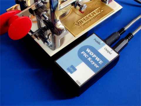
This project was the subject of an article in the Spring 2001 Iowa QRP Journal. The keyer is based on an inexpensive PIC chip and a keyer program that is available on the web. Construction details are presented so that the keyer can be duplicated if desired. The finished product is housed in an off the shelf enclosure that is roughly 2.5" x 1.5" x 1" in size. It has an internal battery and sidetone speaker. Assembly is very simple because the board mounts on internal standoffs and is held in place by the screws that hold the two halves of the enclosure together. The paddle and keyer output connect via board mounted 3.5mm phone jacks, eliminating the need for interconnecting wiring.
This keyer has been the primary keyer at my station since December 2000. I am very happy with the way it operates. It is small, lightweight, and has all the features I need for day to day operation. The standard memories make calling CQ painless and the user programmable memory works great for sending a contest exchange. Because the keyer is always powered by the coin cell, memories and setup parameters are retained when the keyer is not in use.
Keyer Design
This keyer is based on the K1EL design. K1EL offers several keyer kits, pre-programmed PIC chips, and a variety of other interesting products. You can check out the offerings at his web site: "http://www.k1el.com/". To encourage homebrewers, K1EL was nice enough to put the source code for his K8 keyer in the public domain. I programmed a PIC chip with the K8 code but one could also buy a chip from K1EL that has been pre-programmed with the K9 code. The K9 features a faster way to change code speed and a few other options. Both the K8 and K9 have many nice features. The K8 for example has three standard messages built in and two that can be user programmed. It accommodates Iambic mode A and B, can automatically insert appropriate inter letter spacing, has a tune mode, straight key mode, practice mode, and much more. I modified the K8 code slightly to allow another method of code speed adjustment. To learn more about the features of these keyers go to the K1EL web site and download the appropriate manual. I think you will be surprised at the features available in these keyers and the quality of the documentation that K1EL provides.
Below is the schematic of the keyer. The battery is a common CR2032 coin cell and the board is designed to accommodate a battery holder for this part. The CR2032 is rated at 220 mAh. When the PIC chip in not responding to a paddle or pushbutton input, it is in the sleep mode consuming 1uA. When the circuit is active it consumes about 5ma. The battery should therefore provide many hours of active operation and many years of standby operation.
P1 is the connection for the push button switch. Q1 provides keying for the positive keying voltages associated with most modern transmitters. The paddle should be wired to pull the Dit and Dah inputs to ground. The resistors and capacitors on these lines provide the PIC chip with some measure of protection against electrostatic discharge.
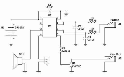
PIC Keyer Schematic
Construction Details
Board Construction
This keyer can be built by making a circuit board from the artwork provided below or you can e-mail me and I will send the it to you as either a .JPG or Circad.PCB file. I made my board using Press-n-Peel. The PCB pattern can be transferred to Press-n-Peel by printing directly on the Press-n-Peel in a laser printer or by copying it to Press-n-Peel using a laser photocopier. The copper clad board should be thoroughly cleaned and free of any residue before attempting to transfer the Press-n-Peel image to the copper. I have found that cleaning the copper with SOS pads was not a good idea. The board looks bright and shiny but the SOS pad leaves a film on the board that the Press-n-Peel will not adhere to. Cleaning the copper with plain steel wool produces excellent results. To transfer the image to the copper, use an ordinary household iron and follow the instructions that come with Press-n-Peel. You may have to experiment to find a temperature setting that provides a good transfer without distorting the image. My experiments indicate that a fairly wide range of temperature settings will provide good results.
When the image is transferred, etch the board as normal. It can then be cut out, drilled, and the copper can be tinned if you desire.The large pads in opposite corners of the circuit board should be drilled out for mounting on the enclosure standoffs. On the prototype I drilled these with a 3/16 inch bit and the board fit nicely.
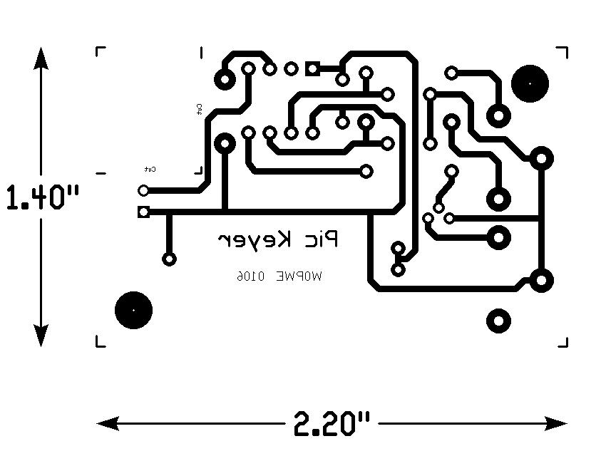
Board Layout
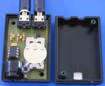
Parts and Board Assembly
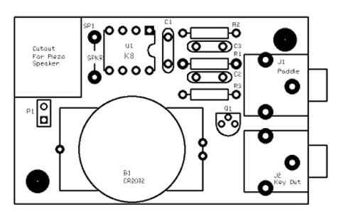
Parts placement guide for the PIC Keyer
PIC Keyer Parts List
| Part |
Description |
| B1 |
CR2032Battery |
| U1 |
PIC12C509 w/K8 or K9 pgm. |
| C1,C2,C3 |
.01µF Ceramic Capacitor |
| J1,J2 |
3.5mm Stereo Jack, Digikey CP-3543N-ND |
| Q1 |
2N2222 NPN Transistor |
| R1,R2 |
330 ohm 1/4W resistor |
| R3 |
4.7K ohm 1/4W resistor |
| SP1 |
Piezo Speaker, Mouser 539-PB1621P |
| Tact Switch |
Digikey SW403-ND |
| Battery Holder |
Digikey BA2032-ND |
| Enclosure |
Mouser 616-71971 |
Enclosure
The holes in the enclosure for the jacks and speaker output are centered on the line where the two halves of the enclosure join. Put the enclosure together and locate the holes relative to the sides as indicated in the drawing. Drill the holes along the joining line.
The square hole in the enclosure top allows a momentary tact switch to be positioned so that its actuator is almost flush with the face of the enclosure. Pressing on the decal above the switch causes it to actuate.
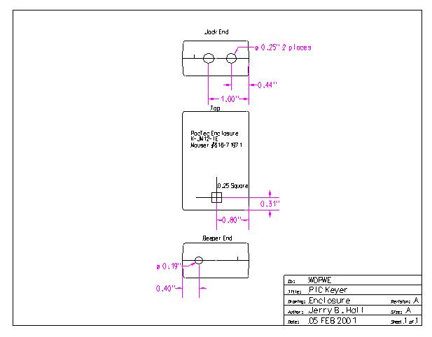
Enclosure for the PIC Keyer
Final Assembly
I wish I could have found a tact switch tall enough to mount on the board and extend through the top of the enclosure. Nothing like that could be found so I made an extender for the switch by cutting a piece of double-sided circuit board material 7/16-inch long by 5/16 inch wide. The switch straddles the edge of the board and its pins are soldered to the copper on each side. Two scrap resistor leads are then soldered into the P1 location on the board and pressed together enough so that the switch extender board can be slid between then and remain in place. The switch is then aligned with the hole in the top of the enclosure, the enclosure top is removed, and the leads are soldered to the switch extender board. An alternative to the decal and tact switch would be to mount a miniature push button switch on the enclosure somewhere and wire it into the P1 location directly or through a small two pin header.
When all the components are mounted on the board it can be placed in the enclosure. The board should sit on the through-hole standoffs and the jacks should extend through the holes leaving the tips of them roughly flush with the end of the enclosure. The speaker can be adjusted slightly so that its output opening lines up with the hole in the enclosure. Install the two screws that hold the enclosure together and the keyer is almost finished.
At this point I chose to finish off the keyer with a decal that labels the input/output jacks and pushbutton position. My daughter and in house graphic artist produced the sticker shown in the photo using Microsoft Publisher. She also made a sticker that lists all the keyer commands and I applied it to the bottom of the enclosure. A strip of "Fun Foam" was also glued to the bottom of the enclosure at each end to help keep it in place on the tabletop.
|
|