
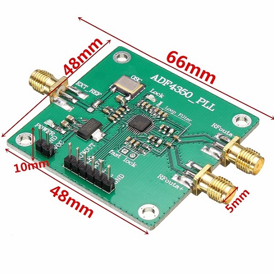
Specifications: Output frequency range: 137 MHz to 4.4 GHz Power supply voltage: 4 ~ 9 V (5V recommended) Output signal: sine wave 2.2 GHz ~ 4.4 GHz (fundamental) 137 MHz to 2.2 GHz square wave (fundamental division) Output signal: Output speed, signal strength: + 5dBm(programmable) RF connector: SMA female head Control interface: Three-wire SPI Reference clock: 10,000 MHZ (default), via interface to an external SMA Size (L * W * H): 66 x 48 x 10 mm NOTE: -Reference Clock The default reference clock signal is active 10,000 MHZ clock, can also be an external reference clock signal, need to use iron to modify the connection mode, connection EXT_REF for external reference signal. -RF Output For the convenience of use, the broadband output is default, the output of two differential signals, can be used to output all the way to use, one can be used to monitor the output. 4351 PLL development board
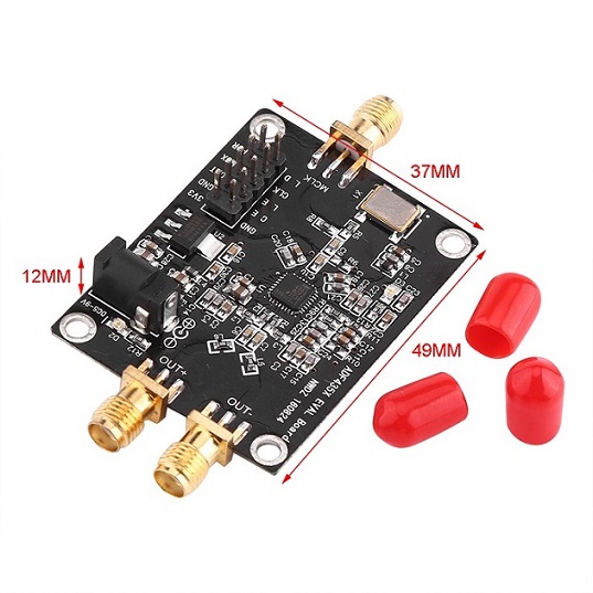
This ADF4351 signal source development board has well designed circuit board layout. It can be controlled by using the official software. All control pins are available for convenient operation. Default + -50ppm 25M active crystal oscillator. Circuit diagram in PDF format and STM32 test program are provided. Three-wire SPI lead to control pin and state locking pin, allowing all functions including point frequency sweep and frequency hopping, stepping to 1K, low frequency step can be 0.1K, according to crystal frequency. Specifications: Output Frequency Range: ADF4351: 35M-4.4G Power Supply: DC002 Interface DC4-9V(typical 5V) Output Signal: 2.2GHz - 4.4GHz fundamental wave (sine wave), 35MHz - 2.2GHz fundamental division (square wave) Signal Output Connector: SMA female Size: 49 x 37 x 12mm / 1.93 x 1.45 x 0.47" File Download: http://pan.baidu.com/s/1o8gBCJS (password: gnxy) ADL5350 Mixer board
The ADL5350 is a high linearity, up-and-down converting mixer capable of operating over a broad input frequency range. It is well suited for demanding cellular base-station mixer designs that require high sensitivity and effective blocker immunity. Based on a GaAs pHEMT, single-ended mixer architecture, the ADL5350 provides excellent input linearity and low noise figure without the need for a high power level local oscillator (LO) drive. In 850 MHz/900 MHz receive applications, the ADL5350 provides a typical conversion loss of only 6.8 dB. The integrated LO amplifier allows a low LO drive level, typically only 4 dBm for most applications. The input IP3 is typically greater than 25 dBm, with an input compression point of 19 dBm. The high input linearity of the ADL5350 makes the device an excellent mixer for communications systems that require high blocker immunity, such as GSM 850/900 and 800 MHz CDMA2000. At 2 GHz, a slightly greater supply current is required to obtain similar performance. The single-ended broadband RF/IF port allows the device to be customized for a desired band of operation using simple external filter networks. The LO to RF isolation is based on the LO rejection of the RF port filter network. Greater isolation may be achieved by using higher order filter networks, as described in the Applications Information section of this data sheet.The ADL5350 is fabricated on a GaAs pHEMT, high performance IC process. The ADL5350 is available in a 3 mm x 2 mm 8-lead LFCSP. It operates over a -40�C to +85�C temperature range. An evaluation board is also available. Specifications: Supply voltage: +5 V DC Broadband radio frequency (RF), intermediate frequency (IF), and local oscillator (LO) ports Conversion loss: 6.8 dB Noise figure: 6.5 dB High input IP3: 25 dBm High input P1dB: 19 dBm Single-ended design: no need for baluns 4GHz Noise Source board
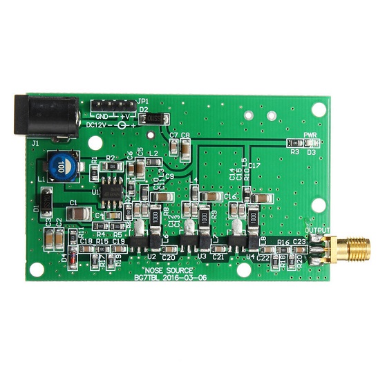
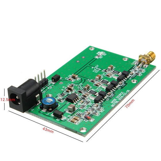
Specifications: Name: White Noise source Power:DC12V/0.3-1A Output Connect:SMA Reference ENR: 0.1G/60DB 0.5G/55DB,1G/52DB, 1.5G/48DB 2G/38DB 2.5G/30DB,3G/27DB,3.5G/20DB ENR (Excess Noise Ratio), noise sources over standard noise temperature T0 thermal noise. Package Contents: 1 x DC 12V Noise Source Simple Spectrum External Generator Tracking Source SMA