|
|
C1 - 44nf C4 - 12nf C2 - 33nf C5 - 8.2nf C3 - 20nf C6 - 4.7nf |
Introduction
The February, 2000 issue of Amateur Radio included my article on An Experimental Low Frequency Transmitter (ref. 1). The article was published in anticipation of the approval of a new amateur band in the LF region. At the time of preparing this article which follows, approval was still being sought. There was also the question that if such a band was approved, would it allow some mode of speech transmission?
In anticipation of a need for speech operation, I decided I would design a speech modulator for the already built LF Power Amplifier. With the limited band space available in a band in this part of the radio spectrum, a single sideband (SSB) system seemed preferable to the wider bandwidth AM system. So this is what I have built and what I am about to describe.
The simplest way to produce SSB for the LF transmitter might have been to heterodyne down the RF output of the amateur station HF transceiver. However this might have put some limitations on the utility of the LF equipment for use at a unique site away from the amateur station and I decided to build a stand alone modulator which could connect into the LF transmitter.
These days, most SSB transmitters use the filter method where double sideband is produced with carrier balanced out and one sideband rejected by feeding the other through a steep skirted bandpass filter. The filter is fixed in frequency and frequency transmitted is derived by a heterodyne process. The filter is normally centred in the HF region and the usual amateur method to make such a filter is to use a ladder network with quartz crystals of the same frequency. For application with the LF transmitter, the fixed frequency SSB signal, could be heterodyned down to the required low frequency.
An alternative method of producing a single sideband is the phasing system. For this system, there are two modulators which balance out the carrier signal fed to them. The carrier to one is fed 90 degrees out of phase to the other. Audio signal generated by speech is fed to both modulators, the signal fed to one being 90 degrees out of phase with the other over the whole speech frequency range. Balancing out of one sideband using this system can be illustrated with the aid of vector diagrams. A description making use of these diagrams, as given in the RSGB Radio Communication Handbook, is included in an appendix at the end of this article.
One feature of the phasing system is that it can be made to operate over a wide range of frequencies without any tuned circuits, selective frequency circuits or heterodyning. For the LF transmitter, this system provided some attraction as the whole process could be done at the LF baseband and cover the whole transmitter frequency range of 160 to 200 kHz without any selective frequency elements.
It seems that the phasing system might have lost favour because of difficulties in making a satisfactory audio phase shift network. Whilst a 90 degrees phase shift can easily be achieved at a single radio frequency, it is somewhat more difficult to maintain a constant 90 degrees phase shift over the whole speech frequency spectrum. Some networks used for the audio phase shift have required high precision components and this has discouraged assembly by radio amateurs. Because of this, my first job was try out an audio phase shift network. As it turned out, this proved to be no problem. Furthermore, I had previously experimented with crystal ladder filters as used in the filter type system (Ref. 2) and my conclusion was that it was simpler to get operating the audio phase shift network in the phasing type system than the ladder filter in the filter type system. Also because of the quartz crystals, the component cost of the ladder filter was greater. With this in mind and with consideration of the advantages discussed in the previous paragraph, I decided to build the modulator around the phasing system and the arrangement figure 2 evolved.
The Audio Phase Shift Network
The circuit of the audio phase shift network used is shown in figure 1. This is a design published in issues of both the ARRL Handbook and the RSGB Radio Communication Handbook and is referred to as the polyphase network by RSGB. Acknowledgement of design is given to M.J.Gingell by RSGB and HA5WH by ARRL. It requires 24 resistors of the same value and 6 different value groups of capacitors, each capacitor in its group the same. This is a lot of resistors and capacitors but according to the documentation, ordinary 10% tolerance components can be used to achieve constant phase shift over the speech range of 300 to 3000 hertz , with a performance of 60 dB of opposite sideband attenuation.
|
|
|
C1 - 44nf C4 - 12nf C2 - 33nf C5 - 8.2nf C3 - 20nf C6 - 4.7nf |
The network is fed from a low impedance balanced source and gives a four phase output of 0, 90, 180, & 270 degrees. From this, two outputs, 90 degrees apart, can be either balanced or unbalanced.
Despite the large number of components, it didn’t take me long to assemble them on a piece of matrix board just as they are laid out in the circuit diagram. I put in a matrix pin for each component junction and soldered the components in. Checking it out over the speech frequency range is simple. An audio oscillator is fed to the input via a balancing transformer. The outputs are checked for correct phasing and equal amplitude using any two of the outputs fed to the two Y inputs of a dual trace CRO. Phasing can be carefully scaled using the CRO graticule. For a single trace, one output can be fed to the X amplifier and the other to the Y amplifier to form a vector trace.
As far as I was concerned, I just wired the right value components in and it all just worked like a charm. So the audio phase shift network was no real problem.
The Single Sideband System
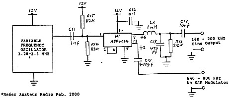
A Block diagram of the single sideband system is shown in figure2.
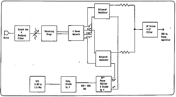
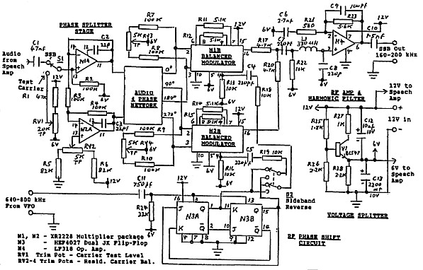
A number of different well known integrated circuit packages such as the MC1496, NE602 and the SL1640 could have been used as balanced modulators. However I happened to have a number of XR2228 Monolithic Multiplier packages and two of these (N1 & N2) are used for these functions. These devices have balanced X and Y input circuits, a balanced output and a circuit arrangement which looked ideal for a balanced modulator. They can also handle frequencies up to around 3 MHz , well above our LF range.
The XR2228 packages also include an operational amplifier each (N1A & N1B) and the pair of these are used to form a balanced low impedance driver for the audio phase network. The amplifier outputs are directly coupled through the network to the X inputs of the balanced modulator sections of the packages (N1B & N2B). Precise DC balance of the complete circuit (necessary to set to for best carrier rejection) is set by trimpot RV2. In retrospect, my thoughts are that it might have been better to use a separate op amp package for the driver as the arrangement resulted in the concentration of a lot of components around the two XR2228 units.
Concerning residual carrier balance, a later addition was the inclusion of trimpots RV3 and RV4 which allow individual adjustment balance of the two balanced modulators and further improvement in the rejection of residual carrier.
A 90 degree phase shift for one of the RF carriers can easily be achieved with simple reactive circuits but this system is somewhat confined to a single frequency. Instead, a circuit using two type D or JK flip-flops can provide two outputs 90 degrees apart for any frequency the flip-flops can handle. For this function, LOCMOS dual JK flip-flop type HEF4027 (N3) has been used. One characteristic of the circuit is that it requires a drive frequency four times the carrier frequency so that for the 160 to 200 kHz transmitter, we need 640 to 800 kHz drive from the VFO. Change between upper and lower sideband is simply achieved by reversing the output leads from N3 which feed the two balanced modulators. Switch S2 is provided for this purpose.
The outputs from the two balanced modulators are combined at the junction of R17 and R20. The single sideband output is insufficient to drive the input of the transmitter and amplifier N4 raises the output level by a factor of 10. The output from the modulators contains higher order frequency components and L1-C8 and R23 -C9 provide a frequency roll-off above 200 kHz to attenuate these components. This is are the only frequency dependent section of the SSB system, limiting operation much above 200 kHz.. Higher order frequency components are further attenuated in the low-pass filter at the output of the transmitter.
As a matter of interest I did carry out some limited tests to see how high a frequency the system could be made to work. (Of course not including the output filters just discussed). I found I could generate single sideband at frequencies as high as 3.5 MHz, limited probably by the characteristics of the XR2228 packages. I suspect the modulators could be made to go higher using packages such as the NE602. Further to that, higher frequencies could be achieved by heterodyning.
The circuit can be switched from SSB to constant carrier for testing or for CW mode by operating switch S1. It achieves this by unbalancing the modulators to allow carrier to get through. The level of carrier is determined by the degree of unbalance set by trim-pot RV1. The switch also disconnects the speech amplifier so that modulation cannot take place. Whilst I haven’t allowed for it in the switching, it is only a matter of shorting out this part of the switch to allow the speech signal to reach the modulators with the carrier on and we generate amplitude modulation.
The Speech Amplifier
The speech amplifier is shown in figure 4. It uses two amplifier stages to raise the speech level from the microphone sufficient to drive the input of N1A in figure 3. Its overall voltage gain is close to 2000. The output level is set by potentiometer RV5 which is mounted as a front panel control of the modulation level. Input sensitivity is suitable for a typical dynamic microphone.
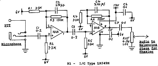
The amplifier also includes second order components to achieve a frequency roll off below 300 Hz and above 3000 Hz. This inclusion of some attenuation outside the normal speech range seemed desirable as the audio phase shift network is designed for constant phase difference between its outputs only over the 300 to 3000 Hz range. If any speech components outside this frequency range pass through the network, the phase relationships could be different which could cause generation of opposite sideband.
A popular choice of an amplifier package for the speech amp would have been the uA747 dual op amp. However I have accumulated a multitude of type LM349M which have four amplifiers in the one package. The only reason I instead selected the LM349 for this circuit is that I thought I had better start making some use of these.
The input connection for a microphone is a tip/ring/sleeve stereo type socket which is my standard for microphones in my shack. The tip is wired to a terminal outlet for use as Push-to-talk (PTT) if required later for receive/transmit control.
Power Rails
The modulator circuitry (figure 3) and the speech amplifier circuitry (figure 4) are operated from 12v derived in the transmitter unit and initially provided just for the VFO. A further rail of 6V is derived by V1 circuit in figure 3 to provide a centre voltage which sets the operating points in the various circuits.
The Variable Frequency Oscillator (VFO)
The VFO is described in my previous article on the transmitter (ref 1). It initially operated at 10 times the transmitted Low Frequency but this was later changed to 8 times. Some time had elapsed between when the transmitter was built and when I decided write about it in AR. I had forgotten about the change and wrote it up in the article as 10 times. However if one carefully examines the divider circuit following the VFO, as published, it is clearly a divide by 8 circuit. My apologies for that error.
Because the RF phase shift circuit in the sideband unit uses an RF drive signal 4 times the suppressed carrier frequency, an output from the VFO is now required at only half the VFO frequency. The original HEF4017 counter was replaced with a HEF4024 counter which was connected to give two outputs, one divide by 2 and the other divide by 8, the latter of which was fed through the existing sine shaping filter. The circuit detail is shown in figure 5. If the new SSB unit is used, the divide by 2 output is connected into RF phase shift flip-flop circuitry input in the modulator. If it is desired to operate the transmitter in its original CW mode and discard the modulator unit, the divide by 8 sine wave output at 160 to 200 kHz can be directly wired to the transmitter power amplifier input.
Alternatively, to operate CW when the modulator is left connected in circuit, switch S1 (figure 3) is operated to generate the 160 to 200 kHz signal fed to the transmitter via the unbalanced modulators.
Hardware
The integrated circuit packages and associated resistors and capacitors are hard wired on matrix board. The unit is mounted in a small metal box with control switches, potentiometer RV5 and the microphone jack, all on the front panel. It is a stand-alone unit so that the transmitter amplifier and VFO can be used with it or without it. This way, the transmitter can be used on its own for its intended earlier purpose as a keyed CW beacon for transmission tests at a suitable site. As a stand-alone unit, the modulator can also be used on any other LF transmitter we might desire to put to air.
A connector strip at the rear of the metal box provides for connection of RF in from the VFO, SSB out to the transmitter amplifier and 12 Volt supply.
Integrated circuit packages used in this project were selected on the basis of them being on hand at the time and may not be readily available from local sources. However there is nothing critical about their selection and if anyone wishes to duplicate the circuitry, there are plenty of alternative packages. For example any general purpose op amp package such as the twin uA747 could be used for the speech amp and following balancing stages. As mentioned before, packages such as the NE602 or MC1460 could be used for the balanced modulator stages. For RF amp V4, a substitute op amp should have a high open circuit gain at 200 kHz. In the case of the digital packages, (the counter and the twin JK flip-flop), CMOS logic was chosen for operation on the 12V rail.
Performance
Peak power output level in the transmitter power amplifier can be achieved with a signal from the output of the modulator of around 6VPP. For this level, an audio level of around 6VPP is required at the input of amplifier N1A (figure 3) and the signal level from the microphone must be not less than 2 mVpp.
With careful adjustment of RV2, RV3 and RV4, the residual carrier level at the output of the transmitter can be set as low as 60 dB below maximum power output. Optimum settings of these controls are slightly different for the upper or lower sideband. However, I imagine that if a band is approved, we would settle on a standard for which sideband is used and I don’t expect there would be a need for regular on air changing between the sidebands.
I haven’t any test figures for opposite sideband rejection. To measure this accurately, one needs a calibrated spectrum analyser which was not available for my tests.
Of course, there are no on air test results as these will depend on approval to transmit or approval of an LF amateur band.
Summary
A Single Sideband Modulator for the Low Frequency (LF) region has been described. The unit was constructed to operate in conjunction with the LF Transmitter previously documented by the writer and published in the February 2000 issue of Amateur Radio. However as a stand-alone unit, it could well be used with any other LF transmitter.
The LF Transmitter as published in Amateur Radio included circuits for DC or tone keying. Detail of the RF driver and power amplifier (without keying circuits) is included in this site. For detail CLICK HERE.
The single sideband system uses the phasing system of balancing out the opposite sideband. The need for precision components in the audio phase shift network in this system is often emphasised as a problem for home constructors. However the writer found that by using the polyphase network, it seemed a lesser task than making operational the crystal ladder filter often used in the filter single sideband system.
A feature of the phasing system is that it does not need tuning or frequency dependent circuits in its generation. The only frequency dependent element in this unit is a low pass filter set to cut off higher order components of frequency above the LF band of operation..
References
1. Lloyd Butler VK5BR - An Experimental Low Frequency (LF) band Transmitter - Amateur Radio, Feb. 2000.
2. Lloyd Butler VK5BR - The Ladder Filter Revived - Amateur Radio, March 1990.
3. Radio Communication Handbook (RSGB), Sixth Edition, Chapter 7 - HF Transmitters and Transceivers.
4. ARRL Handbook for the Radio Amateur, 1989 Edition, Chapter 18 - Voice Communications.
APPENDIX
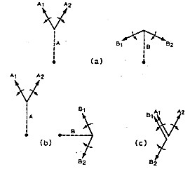
Explanation of Phasing Method of SSB Generation with Vectors (From RSGB Radio Communications Handbook)
For this explanation, reference is made to figure A1. Diagrams (a) show two carriers A and B of the same frequency and phase, one of which is modulated in a balanced modulator by an audio tone to produce contra-rotating sidebands A1 and A2, and the other modulated by a 90 degrees phase shifted version of the same audio tone. This produces sidebands B1 and B2 which have a 90 degree phase relationship with their A counterparts. The carrier vector is shown dotted since the carrier is absent from the output of the balanced modulators. Figure A1(b) shows the vector relationship if the carrier B is shifted in phase by 90 degrees and figure A1(c) shows the addition of these two signals. It is evident that sidebands A2 and B2 are in anti-phase and therefore cancel whereas A1 and B1 are in phase and additive. The result is that single sideboard is produced by this process.