 :
: :
:Introduction
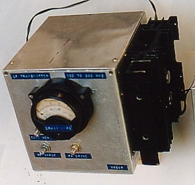
The RF Power Amplifier uses a pair of HEXFET 1 RF430 transistors (V1,V2) operating in a linear mode, push pull class B. The design of the circuit is based on one which I had previously submitted and which was published in AR, November 1989 (ref.1and also on this site). For more detail on the characteristics of the HEXFET transistors and the circuit design, I refer you to that article.
 |
|
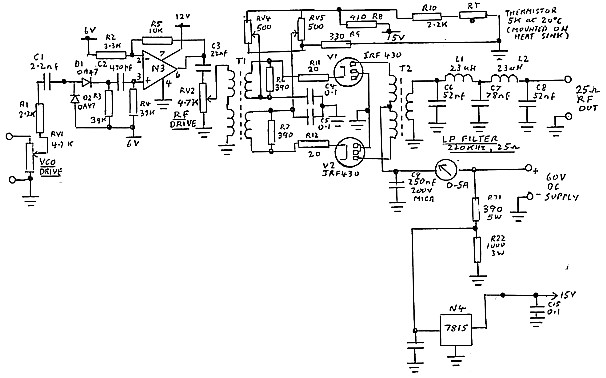
N3 LF310 N4 7815 15V Regulator T1 25 turns, quadfilar wound on Amidon FT150-72 core T2 22 turns, trifilar wound on 620-55254 iron powder core (OD 4cm, ID 2.4cm, Wide 1.5cm, Al = 175mH/1000T) L1, L2 26 turns on Amidon FC334 T130-3 iron powder core. |
Description
Using the output transformer as shown, the amplifier can deliver 70 watts into 25 ohms (or 100 watts into 18 ohms) with an efficiency around 60%. (The remaining 40% is of course heating of the transistors). The transistors are mounted on 6 inches (15.25mm) of Minifin heat sink via berylium insulating washers. With natural convection, the thermal resistance of the Minifin is around 1.3 degrees C per watt and the washers 0.1 degrees C per watt. As such, the temperature rise at the transistor cases could be around 56 degrees for an anticipated heat dissipation of up to 40 watts (continuous signal). This should hold the transistors within their temperature tolerance, but just to make sure, I bolted some extra aluminium fin material to the two sides of the Minifin. In practice operating at 70 watts of continuous output, the transistors run at quite a moderate temperature as felt by the hand. (Of course, in keyed operation the average output power and heat dissipation is even much less).
Static drain current (no signal) is set to 150mA per transistor (300 mA total) with trim pots RV4 and RV5 which control the forward bias voltage. Thermistor Rt is mounted in direct thermal contact with the heat sink and connected in the gate bias circuit. This reduces bias as the temperature rises to hold static drain current reasonably constant with temperature rise. The need for this was explained in Reference 2. At full power of 70 watts loaded into 25 ohms, total drain current rises to around 2 amps.
The RF output is fed via a 5th order Chebychev 220 kHz low pass filter designed for the 25 ohm load. Theoretical attenuation at the first octave in this type of filter is in the order of 50 dB and harmonic radiation could be expected to be more than 70 dB below carrier level.
The nominal drain supply for the output transistors is 60 volt D.C. This is dropped down to 15V via regulator N4 for the gate bias supply.
For notes on Antenna Loading and Tuning,Click Here
References
1. Rf Power Linear Amplification using the IRF Mosfet Transistors - Lloyd Butler VK5BR - Amateur Radio, November 1989.
2. An ExperimentalLow Frequency Band Transmitter - Lloyd Butler VK5BR - Amateur Radio, February 2000.