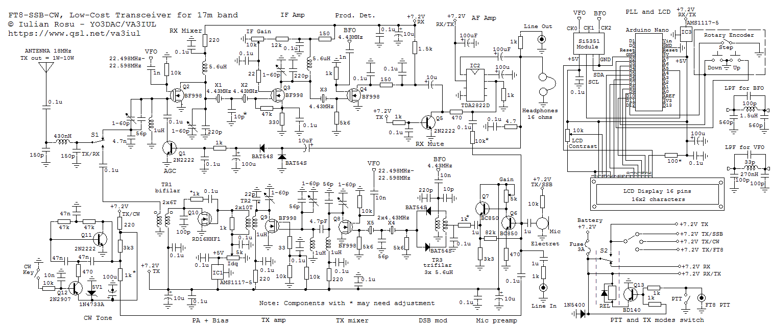
FT8-SSB-CW, Low-Cost Transceiver for 17m band
Iulian Rosu, YO3DAC / VA3IUL, http://www.qsl.net/va3iul
This low-cost transceiver was designed to work with very low DC supply voltage. In receive mode the radio works fine down to 3.8V supply voltage (including the LCD display and PLL). The entire transceiver (RX and TX) works fine when is DC supplied in the range of 5V to 12V (TX out = 1W-10W), which makes it to be a good candidate for portable applications.
The total current consumption in receive mode (including the LCD display and PLL) is about 70mA at 7.2V.
The transceiver is operating on 17m band (18MHz), which is one of the most used bands for FT8 DX QSOs, in these poor propagation times that we pass. Here is a 20m version of the transceiver.
The schematic tries to minimize the number of the components, especially of the “hard to get” variable inductors. There are no variable inductors in this transceiver. The LC resonant tuning is done using fixed value inductors and trimmer capacitors.
For filtering were used five 4.43MHz crystals, three in the receiver and two in the transmitter.
Schematic description
In receive mode, the signal from the antenna goes to the gate 1 of the dual-gate MOSFET transistor Q2 (BF998), which is the receiver mixer. Can buy the transistor from here. If get the MOSFET BF998R (Reverse) the pins of the transistor need to be bended and the transistor soldered on the PCB flipped up side down. On gate 2 (of the same MOSFET) is introduced the VFO signal coming from the PLL synthesizer module. The super-heterodyne receiver use a high-side injection, and for 17m band, the frequency range of the VFO signal is between 22.498 MHz and 22.598 MHz.
At the drain of the mixer transistor Q2 the IF signal (on 4.43MHz) is selected by an LC resonant circuit and fed further to a two-crystal ladder filter. The receiver bandwidth can be slightly adjusted changing the value of the 10pF capacitor placed between the crystals X1 and X2.
The following MOSFET Q3 (BF998) it is a variable IF gain amplifier. At its output the received signal is filtered and further injected to the gate 1 of the Product Detector Q4 (BF998). Gate 2 of the same MOSFET gets the BFO signal (on 4.43MHz) from the PLL synthesizer.
The resulting audio signal at the output of the product detector Q4 is RC filtered and amplified by the TDA2822D audio amplifier (in SO8 package, which can get from here). This IC audio amplifier has better performances compared to the common LM386, and works fine at very low supply voltages, 1.8V up to 15V.
Q1 transistor (2N2222) and a couple of Schottky diodes BAT54S, forms a simple but useful AGC circuit. BAT54S (two diodes in the same package) can get from here.
The gain of the receiver could be also adjusted manually by a 10k potentiometer placed on the gate 2 of the IF amplifier Q3.
In TX mode the receiver is silenced by the Q5 transistor and afferent components.
At the output of TDA2822D circuit, the received audio signal goes to the headphones (16 ohms impedance) and to the line-out connector, in FT8 mode.
In TX mode the signal from the microphone (in SSB mode), from the CW tone generator (in CW mode), or from line-in connector (in FT8 mode), is amplified by the feedback audio amplifier, Q6 and Q7.
Further, the modulation signal goes to the DSB (Double Side Band) modulator, made with TR3 transformer and two BAT54 Schottky diodes. The DSB modulator is also injected with the BFO signal (4.43MHz) from the PLL synthesizer module. If use a BAT54S (two diodes in the same package) the rejection of the carrier is better than 40dB.
Further, the double side band signal goes to a two-crystal ladder filter for removing the lower side band of the signal. After that the signal goes to the TX mixer transistor Q8 (BF998). In gate 2 of Q8 dual-gate MOSFET is injected the signal from the VFO, which is coming from the PLL synthesizer module.
The resulting signal at the output of the TX mixer is filtered by two LC resonant circuits, and amplified by Q9 dual-gate MOSFET BF998.
The last stage of the transmitter is the power amplifier Q10 which is a RD16HHF1 MOSFET. Can get the transistor from here. Another option is to use an RD15HVF1 MOSFET (this is a VHF version but works fine in HF). Can get the transistor from here. RD15HVF1 have 2dB less gain than RD16HHF1, but the output power is similar.
Mitsubishi recommend for RD16HHF1 transistor a quiescent current (idle) of 500mA at 12V operation. I found that the transistor works fine with Idq = 300mA when is supplied at 7.2V. The gate bias (Idq current) is set by a 5k potentiometer supplied with a DC voltage from IC1 (AMS1117-5V regulator). An RC series feedback network (1k* adjustable resistor and 0.1uF capacitor) connected between the gate and the drain of the transistor is used to prevent auto-oscillations of the power amplifier. The TR1 transformer provides the output impedance matching of the power amplifier. The output TX signal is low-pass filtered before going to the antenna.
The PLL synthesizer was made using a Si5351 module, an Arduino Nano board, a Rotary Encoder for frequency tuning, and an LCD display. The Si5351 module can get from here. The output of the Si5351 module are square wave signals. For this project (which use dual-gate MOSFET mixers) is good to use low pass filters at the output of the PLL module, to make the signals sinusoidal. On the schematic of the PLL and LCD is shown also the low-pass filters that were used for VFO and BFO. The PLL, the Arduino Nano, and the LCD display, are DC supplied from IC3 (AMS1117-5V regulator). The PLL synthesizer design is based on AK2B project, updated Arduino Code and Libraries, which works very well for a single band transceiver. The start-up frequency of the PLL, is set to be 22.53MHz (to receive FT8 frequency on 18.100MHz). As a remark, this PLL circuit has much lower output spurious emissions than most of the DDS modules on the market. A DDS module, whatever filtering use at the output, still has "near the carrier" spurs which cannot be filtered easily. However, DDS has much lower phase noise than a PLL, which can make a difference getting the best receiver sensitivity and lowest receive noise floor . An option to filter out the DDS spurs is to place the DDS circuit inside of a PLL loop (as most of the commercial transceivers does) but this will increase the cost of the circuit.
The transceiver circuit was built using SMD components. The components that are not SMD are: the PA transistor RH16HHF1 (which needs to be placed on a heatsink), the PTT transistor, the trimm capacitors, the TR1,TR2,TR3 transformers, the 1uH and 5.6uH inductors, the Si5351 PLL module, the Arduino Nano module, and the relay (Antenna and TX/RX). Those components were added on the main PCB as through-hole components.
The 7.2V battery is a Power Bank USB battery used for charging mobile phones. There are models on the market that goes up to 30A. Most of these power bank batteries use inside six 1.2V rechargeable elements put in series. To get the voltage of 7.2V necessary to supply the transceiver, have to connect two wires (+ and -) across those batteries. For recharging the battery use the same internal circuit fed via USB from a 5V USB charger. A 3A fuse is mandatory to be in place in series with the (+) wire connected to the battery pack.
Transformer TR1 was made on Amidon FB-43-7351 or on a binocular ferrite Amidon BN-43-3312, and transformers TR2 and TR3 were made on Amidon FB-43-2401 or on a binocular ferrite Amidon BN-43-3402.
On the front panel of the transceiver box will be mounted: the IF Gain potentiometer, the Microphone Gain potentiometer, the frequency tuning encoder, the LCD contrast potentiometer, and the TX modes switch (SSB,CW,FT8).
On the back panel of the transceiver box will be mounted connectors for: Antenna (BNC), PTT (3.5mm connector), CW Key (6mm audio connector), Line In (Cinch) and Line Out (Cinch).
Inside of the transceiver box was also placed a "Super Simple CW Keyer" using an Arduino Nano board, based on the project of KB9RLW. If you want a better performance keyer (iambic, memories, PS2 keyboard interface, etc) you can build the K3NG keyer, also based on Arduino Nano.
If for some reason you don't have access to any link mentioned in above text, send me an email and I will provide the requested information.
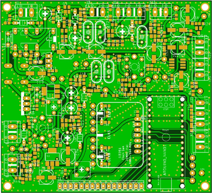
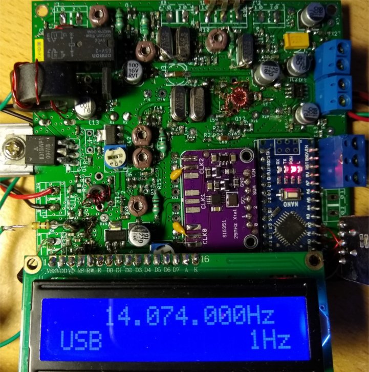
Top view of the PCB layout Transceiver prototype - 20m version