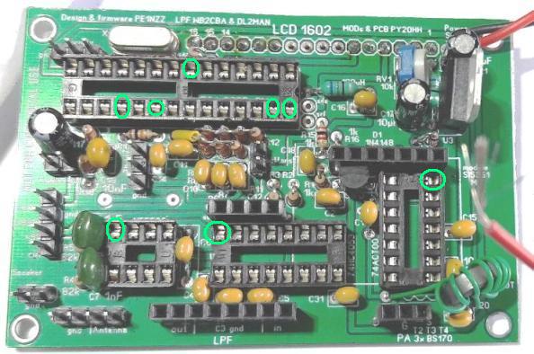
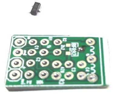
µSDX
MUTIRÃO PASSO A PASSO
µSDX BUILDING STEP BY STEP
The translation was by google ... strange things can appear in English.
Sorry!
Esquema
Scheme
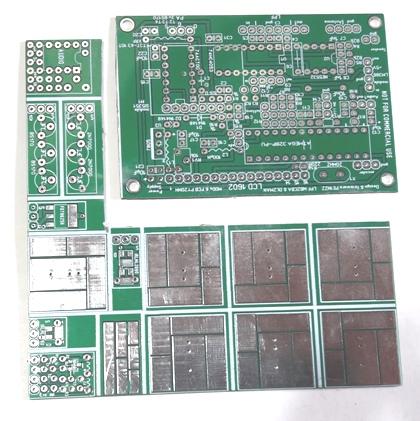
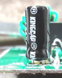
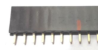
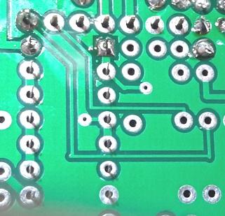
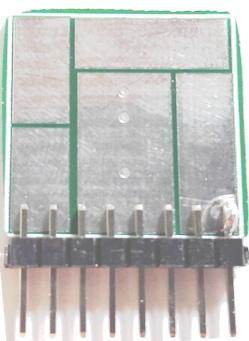
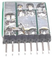
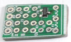
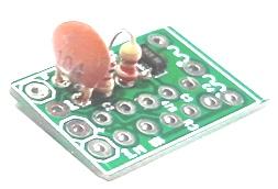
PCB (10x10cm) :
Cortando a PCB
Cutting the PCB
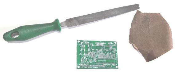
Ferramentas usadas
TOOLS
A serra manual usada pode ter a lamina de serra para cortar
ferro ou de aluminio (que aparece solta) . Uma madeira para fixar sem
danificar a PCB. Um sargento ou um grampo de marceneiro. Prender a PCB
em uma mesa, com a madeira por cima e fixar com o sargento, orientando
a PCB para que o corte fique livre e reto. Aperte bem para não
que a PCB não se mexa enquanto é cortada. Corte
devagar observando a linha de corte sobre a linha branca da PCB.
The hand saw used can have the saw blade to cut iron or aluminum
(which appears loose). A wood to fix without damaging the PCB. A clamp
or a joiner's clamp. Fix the PCB on a table, with the wood on top and
fix it with the clamp, orienting the PCB so that the cut is free and
straight. Tighten tight so the PCB doesn't move while it's being cut.
Cut slowly observing the cut line over the white line of the PCB.
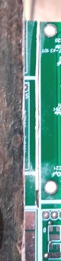
Observe na foto que eu desviei um pouco, mas sem problemas.
Notice in the photo that I deviated a little, but no problem.
posicionando para o proximo corte :
positioning for the next cut:
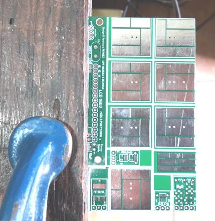
Corte feito !
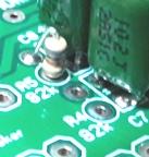
Cut done! Main PCB (78x56mm)
Agora é só rebarbar, eu usei uma lima plana
(não sei o tipo rerere deve ser bastarda) e uma lixa para
pintura poderia ser para ferro grana #100 a #200.
Now it's just deburring, I used a flat file (I don't know the
rerere type must be bastard) and a sandpaper for painting could be for
iron #100 to #200 grit.
Vamos a soldagem
let's solder
Ferramentas que eu uso normalmente :
Tools I usually use:
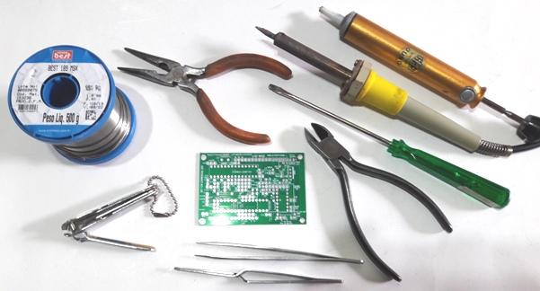
Solda #1mm azul 60%Sn 40%Pb, alicate de bico reto, ferro de solda
Hikari 30W (se for comprar compre umas 2 ou 3 pontas de reserva),
sugador de solda (para remoção de compoenentes ... errar
é humano), cortador de unha parrudo para cortar excesso dos fios
soldados, pincas de aço inox normal e tipo tesoura (normalmente
fechada rerere), alicate de corte (este é Crescent não
precisa ser tão bom...) e uma chave de fenda.
#1mm blue solder 60%Sn 40%Pb, straight-nose pliers, Hikari 30W
soldering iron (if you are going to buy, buy 2 or 3 spare tips), solder
sucker (to remove components... to err is human) , heavy nail clipper
to cut excess welded wires, normal stainless steel tweezers and
scissors type (normally closed rerere), cutting pliers (this is
Crescent doesn't have to be that good...) and a screwdriver.
Eu uso muito a pinça
tipo tesoura, para segurar os componentes e não queimar os
dedos, para SMD uso a pinça normal.
I use the scissor tweezers a lot, to hold the components and not burn
my fingers, for SMD I use the normal tweezers.
Vamos soldar :
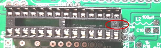
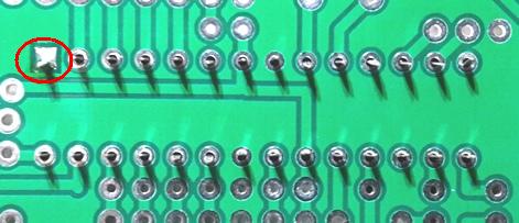
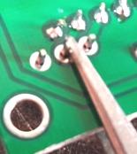
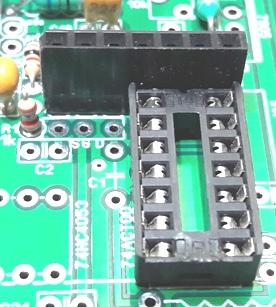
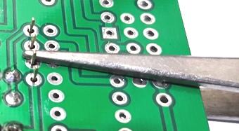
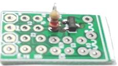
1. Soldando o soquete do Atmega328,
Posicionar o chanfro ou rasgo indicando a posição do pino
1, do soquete e da placa na mesma posição.
Let's solder:
1. Soldering the Atmega328 socket,
Position the chamfer or slot indicating the position of pin 1, socket
and plate in the same position.
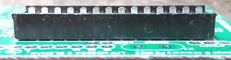
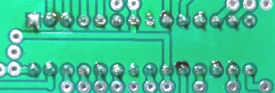
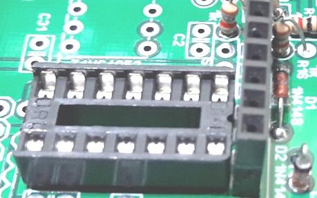
Colocar o soquete verificando se TODOS os pinos estão passando
pelos furos (algum pode dobrar).
Soldar apenas um pino de um dos cantos do soquete.
Insert the socket making sure that ALL the pins are going through the
holes (some may bend).
Solder just one pin from one of the corners of the socket.
Verificar se o soquete ficou junto da placa.
Check that the socket is close to the board.
Se não ficou bom aqueça o pino soldado e junto force o
soquete a ficar na posição desejada.
Se OK , solde o restante dos pinos, com cuidado para não
ocasionar curtos entre ligações.
If it was not good, heat the welded pin and together force the socket
to be in the desired position.
If OK, solder the rest of the pins, being careful not to cause shorts
between connections.
OBS. as soldas ficaram boas, mas na foto não hi!
NOTE the welds were good, but not in the photo!
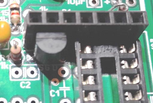
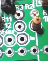
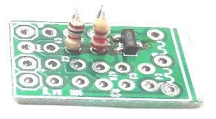
2. Soldar o cristal de 20MHz e o resistor de 220R R14, que tem a
função de limitar a corrente do leds do LCD.
Tanto o cristal como os resistores soldados em pé devem ser
soldados um só terminal, e este terminal deve ser puxado e
reaquecido para ficar no lugar correto, ou seja proximo a PCB.
Solde o cristal com os 20MHz voltados para baixo.
Solde o resistor com a faixa de multiplicação para baixo
(neste caso a faixa marrom).
2. Solder the 20MHz crystal and the 220R R14 resistor, which has the
function of limiting the current of the LCD LEDs.
Both the crystal and the standing soldered resistors must be soldered
to a single terminal, and this terminal must be pulled and reheated to
be in the correct place, ie close to the PCB.
Solder the crystal with the 20MHz facing down.
Solder the resistor with the multiplication band down (in this case the
brown band).
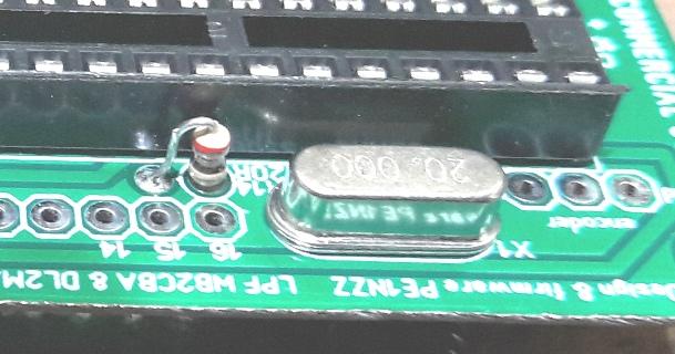
Visto por baixo
seen from below
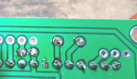
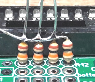
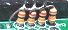
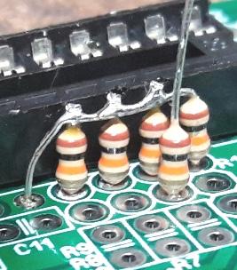
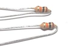
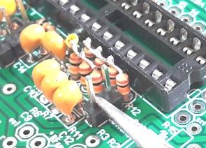
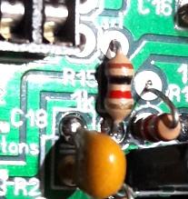
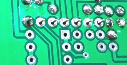
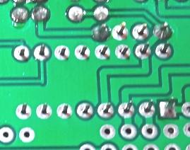
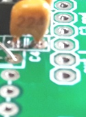
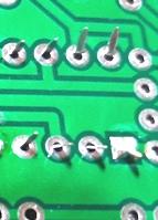
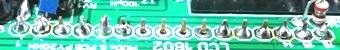
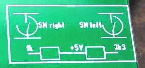
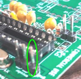
3. Vamos soldar estes 4 resistores R12, R10, R7 e R9 (todos de 10k)
onde todos formam
divisores de tensão, o resistor R12 que vai ligado aos
botões de comando formam um divisor (com os resistores de 1k e
3k3) que fornece uma tensão para o Atmega indicando qual
botão foi acionado (swi, sw2 ou chave do encoder). Já os
outros resistores formam um divisor simples (com outro resistor de
mesmo valor para o 5V) para obter metade da tensão de trabalho
(5V / 2 = 2,5V) assim podendo receber tensões de +2,5 a
-2,5V, ou seja sinais de AC (audio).
Tivemos problemas com as fotos SRY ... temos somente fotos com
todos os 4 resistores soldados.
Solde um resistor por vez.
Procure colocar a faixa laranja para baixo.
Solde um terminal e puxe o resistor pelo rabicho até ficar na
posição desejada.
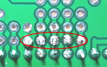
Solde os terminais restantes como na foto e ligue ao terminal a
esquerda (terra).
3. Let's solder these 4 resistors R12, R10, R7 and R9 (all 10k) where
they all form voltage dividers, the resistor R12 that is connected to
the command buttons form a divider (with the 1k and 3k3 resistors) that
provides a voltage to the Atmega indicating which button was pressed
(swi, sw2 or encoder switch). The other resistors form a simple divider
(with another resistor of the same value for 5V) to obtain half of the
working voltage (5V / 2 = 2.5V) thus being able to receive voltages
from +2.5 to -2.5V, ie AC (audio) signals.
We had problems with the SRY pictures... we only have pictures with all
4 resistors soldered.
Solder one resistor at a time.
Try to put the orange strip down.
Solder one terminal and pull the resistor through the tail until it is
in the desired position.
Solder the remaining terminals as in the photo and connect to the left
terminal (ground).
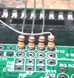
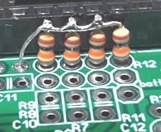
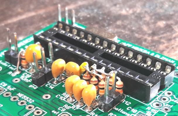
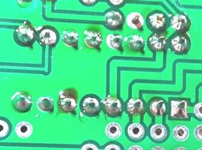
4. Soldando os 3 resistores do divisor R8, R6 e R11 (10k).
Solde um
resistor por vez.
4. Soldering the 3 divider resistors R8, R6 and R11 (10k).
Solder one resistor at a time.
Procure colocar a faixa laranja para baixo.
Soldar um terminal e puxe o resistor pelo rabicho até ficar na
posição desejada.
Try to put the orange strip down.
Solder one terminal and pull the resistor by the pigtail until it is in
the desired position.
Soldar os tres resistores e interligue eles como foi feito nos 4
rssitores anteriores.
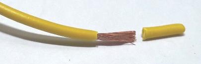
Vamos isolar o fio a ser soldado, corte o isolante de um fio
Solder the three resistors and interconnect them as was done in the
previous 4 resistors.
Let's insulate the wire to be soldered, cut the insulator from a wire
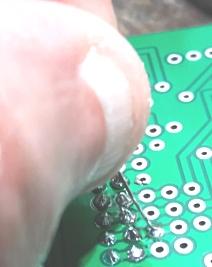
Coloque este isolante (espaguete) no terminal dos resistores a ser
soldado
Place this insulator (spaghetti) on the resistor terminal to be soldered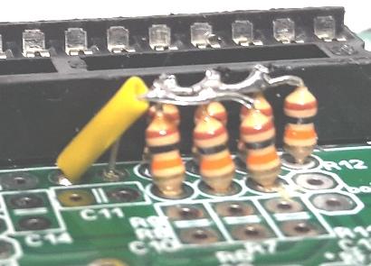
Solde os terminais restantes como na foto e ligue ao terminal a
esquerda conforme foto.
Place this insulator (spaghetti) on the terminal resistor to be soldered
4. Soldar R13 (10k) bias para o microfone.
4. Solder R13 (10k) bias to the microphone.
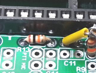
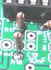
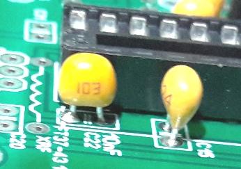
5 Soldar R17 e R18 (10k) filtro passa baixas (junto com capacitor de
103) para eliminar sinal de AC do PWM.
Dobre os terminais antes de montar
5 Solder R17 and R18 (10k) low pass filter (along with 103 capacitor)
to eliminate AC signal from PWM.
Bend the terminals before assembling
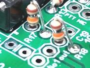
Monte R17 e solde
Mount R17 and solder

Monte R18 e solde
Assemble R18 and solder
R17 e R18 montados
R17 and R18 assembled
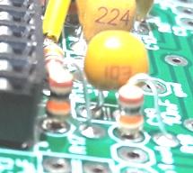
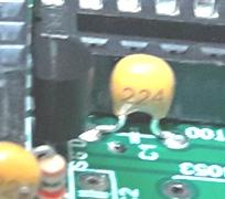
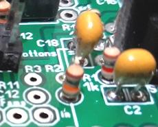
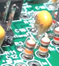
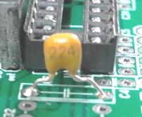
6. Soldando C14 (220nF) filtro DC.
6. Soldering C14 (220nF) DC filter.
7. Soldando C19 (10nF) Filtro do PWM
7. Soldering C19 (10nF) PWM Filter
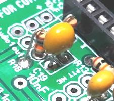
R17, C19 e R18 formam o filtro de PWM, que gera uma tensão DC,
que é o Bias do PA.
R17, C19 and R18 form the PWM filter, which generates a DC voltage,
which is the Bias of the PA.
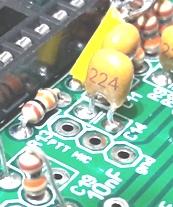
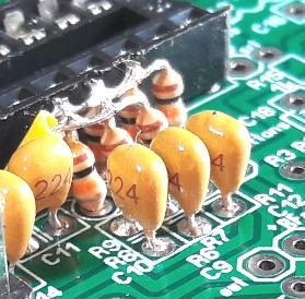
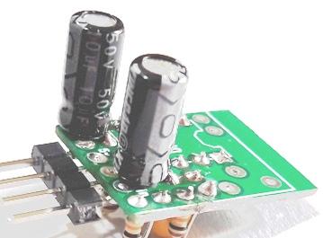
8. Soldando C11 (Filtro DC) , C9 e C10 (by pass audio RX), C12 (by pass
microfone) todos de 220nF. Observe que estão voltados para a
mesma direção.
8. Soldering C11 (DC Filter), C9 and C10 (RX Audio Bypass), C12
(Microphone Bypass) all at 220nF. Note that they are facing the same
direction.
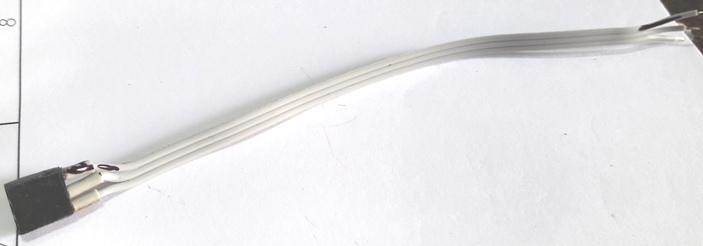
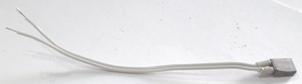
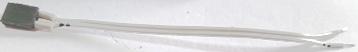
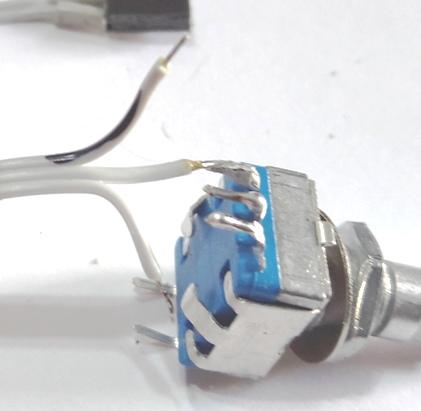
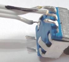
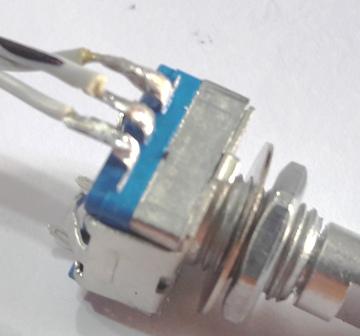
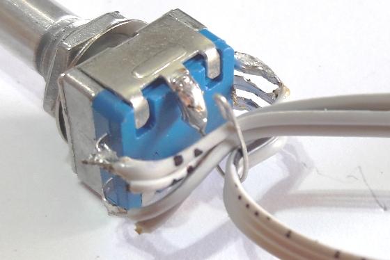
9. Soldando conector para encoder
Nota : caso o colega queira soldar diretamente os fios é uma
opção, eu prefiro conector (tem material no kit).
Para soldar o terminal e 3 pinos é necessario segurar e soldar,
eu uso a pinça tesoura
9. Soldering connector for encoder
Note: if the colleague wants to directly solder the wires, it is an
option, I prefer a connector (there is material in the kit).
To solder the terminal and 3 pins it is necessary to hold and solder, I
use the scissors tweezers
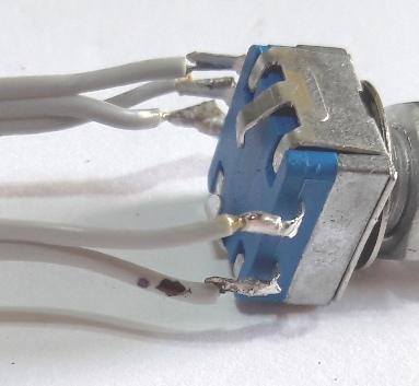
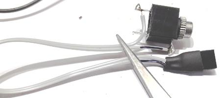
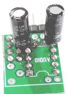
10. Soldando terminal Saida de audio 1
10. Soldering terminal Audio output 1

11. Soldando terminal de microfone (3 pinos).
11. Soldering the microphone terminal (3 pins).
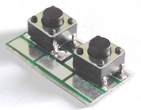
12. Soldando terminal de botões (2 pinos)
12. Soldering button terminal (2 pins)
XXXXXXXXXXXXXXX
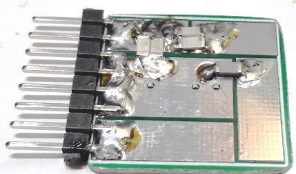
Como estamos até agora :
How we are so far:
xxxxxxxxxxxxxxxxxxxxxxxxxxxxxxxxxxxxxxxxxxxxxxxxxxxxxxxxxx
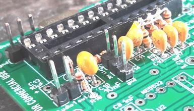
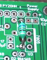
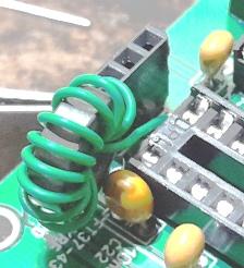
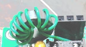
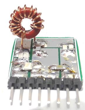
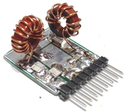
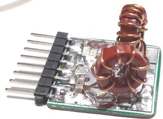
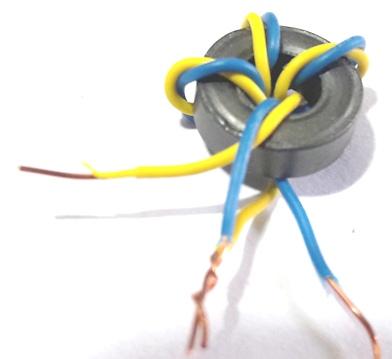
13. Vamos soldar os indutores L1 e L2
Observe que eu não tenho indutores de 100µH, mas
serve de 47 a 120µH, usei 68µH.
L1
13. Let's solder the inductors L1 and L2
Note that I don't have 100µH inductors, but it works from 47 to
120µH, I used 68µH.
L1
L2
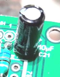
14. Soldando C21
C21 10µF que tem a finalidade de aterrar toda AC ou RF na
linha.
14. Welding C21
C21 10µF which is intended to ground all AC or RF on the
line.
C21
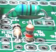
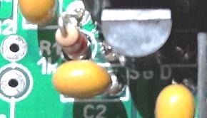
15. Soldando R15 e R16 (1k)
15. Welding R15 and R16 (1k)
R15
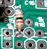
R16
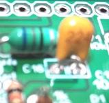
16. Soldando C16 (220nF)
16. Welding C16 (220nF)
17. Soldando C18 (220nF)
17. Welding C18 (220nF)
18. Soldando D1 e D2 (1N4148) (importante: observe a faixa preta na
montagem).
18. Welding D1 and D2 (1N4148) (Important: Note the black band on the
assembly).
D1
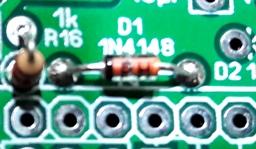
D2
19. Montando R1
19. Assembling R1
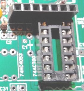
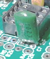
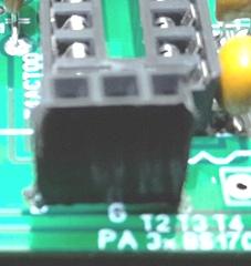
20. Montando Soquete para SI5351 (o si5351 tem a função,
em recepção, de gerar dois sinais na mesma frequencia
defasados em 90 graus, que vão para o misturador 74HC4053 para
detecção do SSB. Em TX ele gera um sinal de CW ou em SSB
com uma variação de frequencia em função do
sinal de audio do microfone, que pode ser positiva ou negativa - USB ou
LSB, comandada pelo Atmega328)
20. Assembling Socket for SI5351 (si5351 has the function, in
reception, of generating two signals at the same frequency shifted by
90 degrees, which go to the 74HC4053 mixer for SSB detection. In TX it
generates a CW signal or in SSB with a frequency variation depending on
the microphone's audio signal, which can be positive or negative - USB
or LSB, controlled by the Atmega328)
Cortando, um pino sempre se perde no corte.
When cutting, a pin is always lost in the cut.
O corte fica irregular é necessario rebarbar com uma faca ou lima
The cut is uneven, it is necessary to deburr with a knife or file
Ok pronto
OK ready
Eu fixo o soquete com a pinça auto travante
I fixed the socket with the self-locking collet
Soldar apenas um terminal para fixar
Solder only one terminal to fix
Monte o soquete de 14 pinos, sem soldar, ele é importante pois
na colocação do CI temos interferencia mecanica. Observe
sempre o sinal do primeiro pino do CI.
Mount the 14-pin socket, without soldering, it is important because in
the placement of the IC we have mechanical interference. Always observe
the signal of the first IC pin.
Monte o CI
Mount the IC
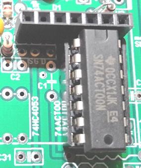
Observe na foto que a interferencia
Note in the photo that the interference
Solde dois pontos do soquete de 14 pinos, IMPORTANTE verificando a
posição do pino1
Solder two points of the 14 pin socket, IMPORTANT checking the position
of pin1
Podemos soldar todos os pinos, do soquete do SI5351.
We can solder all pins, from the SI5351 socket.
e do CI
74ACT00. O 74ACT00 tem a função de driver para o PA
ele aumenta a tensão de RF do SI5351 de 3.3V para 5V com maior
potencia (corrente).
and the CI 74ACT00. The 74ACT00 has a driver function for the PA it
increases the RF voltage of the SI5351 from 3.3V to 5V with higher
power (current).
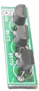
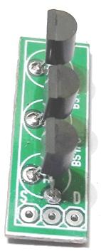
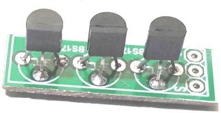
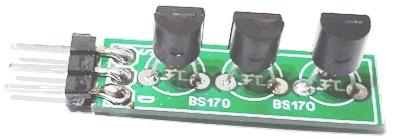
21. Soldando BS170 que atua como chave de TX RX
21. Welding BS170 that acts as a TX RX switch
22. Soldando C1, que é usado como passagem da RF e impedimento
da corrente continua.
22. Welding C1, which is used as RF pass and direct current impediment.
23. C2 tem a mesma função de C1.
23. C2 has the same function as C1.
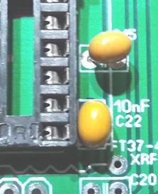
24. C15 (220nF) e C22 (10nF)... C15 tem a função de
eliminar apresença de RF na linha de alimentação e
C22 acopla o driver (74ACT00) ao PA e é usado tambem para
filtrar o PWM na linha do gate do PA sendo importante manter este valor
10nF.
24. C15 (220nF) and C22 (10nF)... C15 has the function of eliminating
the presence of RF in the supply line and C22 couples the driver
(74ACT00) to the PA and is also used to filter the PWM in the gate line
of the PA being important to keep this value 10nF.
25. Montando R2 e R3. O resistor R2 e R3 formam um divisor de
tensão na entrada do mixer de tal forma que sinal de AC de
amplitudes positivas ou negativas possam ser amplificadas.
25. Assembling R2 and R3. Resistor R2 and R3 form a voltage divider at
the input of the mixer so that an AC signal of positive or negative
amplitudes can be amplified.
R2
R3
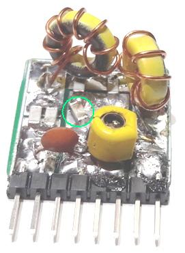
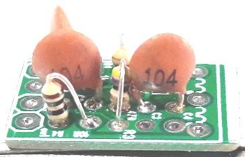
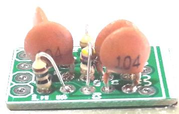
26. Soldando o soquete para o amplificador de RF. Caso o USDX seja para
40 e/ou 80m apenas, colocar um fio jumpeando a entrada com a
saida (primeiro e ultimo pino). O amplificador de RF deve ser usado
apenas para frequencias acima de 14MHz em frequencias menores o uso
dele causa distorção e excesso de sinal.
26. Soldering the socket for the RF amplifier. In case the USDX is for
40 and/or 80m only, place a wire bridging the input with the output
(first and last pin). The RF amplifier should only be used for
frequencies above 14MHz at lower frequencies its use causes distortion
and excess signal.
Fixando
fixing
Fixando
fixing
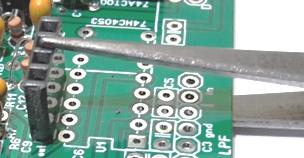
Monte o soquete do 74HC4053 (16 pinos) observe pino 1. Solde o soquete
do amplificador deRF
Mount the 74HC4053 socket (16 pins) note pin 1. Solder the RF amplifier
socket
Solde os pinos do soquete de 16 pinos
Solder the 16-pin socket pins
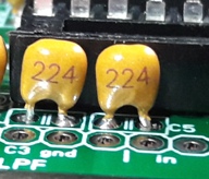
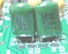
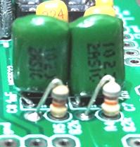
27. Montando C3, C4, C5 e C6
C3, C4, C5 e C6 tem a função de eliminar a RF preseente
na linha e preservar o sinal de audio.
27. Assembling C3, C4, C5 and C6
C3, C4, C5 and C6 have the function of eliminating the RF present in
the line and preserving the audio signal.
C6
C4
C3
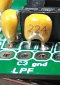
C3 e C5
28. Montando o soquete do NE5532 (8 pinos).
O NE5532 tem a função de amplificar o audio presente em 4
entradas. O ganho é bem elevado.
28. Assembling the NE5532 socket (8 pins).
The NE5532 has the function of amplifying the audio present in 4
inputs. The gain is very high. .
Observe o pino 1 na montagem
Note pin 1 on assembly
Solde sempre um pino e confira se esta tudo certo e solde os outros
pinos.
Always solder a pin and check if everything is ok and solder the other
pins.
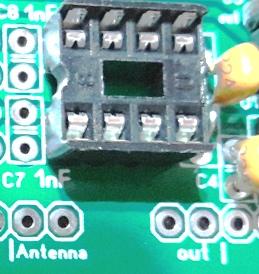
29. Montando C7 e C8 de 10nF (102).
C7 e C8 tem a função de limitar a faixa passante do
amplificador, deixando passar apenas sinais de media e baixa
frequencia. Montei o 10nF de poliester que pode ser usado nesta
aplicação no kit é de multicamada
29. Assembling 10nF C7 and C8 (102).
C7 and C8 have the function of limiting the amplifier's passband,
allowing only mid and low frequency signals to pass. I mounted the 10nF
of polyester that can be used in this application in the kit is
multilayer
C7
C7 e C8
30. Montando R4 e R5 82k 1%
R4 e R5 são de 82K 1% ...o uso de 1% é que o material
empregado na fabricação do ressitor gera menor ruido em
funcionamento. Usei na montagem resistores de 10%,
não percebo diferenças (SRY não tinha disponivel
de 1%).
30. Mounting R4 and R5 82k 1%
R4 and R5 are 82K 1% ...the use of 1% is that the material used in the
manufacture of the resistor generates less noise in operation. I used
10% resistors in the assembly, I don't see any differences (SRY didn't
have 1% available).
R5 e R4
R5
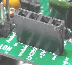
31. Soquete para o modulo do amplificador de audio (4 pinos).
O amplificador de audio é opcional, sem ele temos um sinal
compativel para fones ou para um pequeno autofalante, o sinal presente
tem junto PWM de cerca de 50kHz que pode influir no funcionamento (nem
todo o autofalante ligado sem o amplificador funciona). Com o
amplificador de audio eliminamos o sianl do PWM e temos um audio com
maior volume e sem problemas com impedancias de autofalante.
Aqui cometi um gato soldei o conector macho ao inves da femea ...na
foto aparece o femea (que só descobri ao colocar o modulo do
amplificadorde audio) ...mas em outras fotos seguintes o conector macho
pode aparecer.
31. Socket for the audio amplifier module (4 pins).
The audio amplifier is optional, without it we have a compatible signal
for headphones or a small speaker, the present signal has a PWM of
about 50kHz that can influence the operation (not all speakers
connected without the amplifier work). With the audio amplifier we
eliminate the PWM signal and we have an audio with greater volume and
without problems with speaker impedances.
Here I made a cat I soldered the male connector instead of the female
one ...the female connector appears in the photo (which I only
discovered when I placed the audio amplifier module) ...but in other
following photos the male connector may appear.
32. Saida de audio 2
A saida de audio 2 é a saida do audio amplificado. Propria para
auto falante pequeno..
32. Audio output 2
Audio output 2 is the amplified audio output. Suitable for small
speaker..
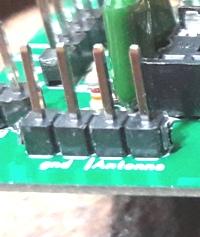
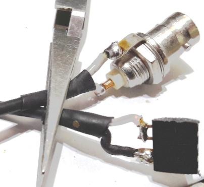
33. Conexão de antena.
A conexão de antena pode ser feita diretamente com cabo coaxial
fornecido no kit, mas podemos usar um soquete ou plug.
33. Antenna connection.
The antenna connection can be made directly with the coaxial cable
provided in the kit, but we can use a socket or plug.
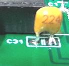
34. Capacitor C31 220nF (224).
Este capacitor aterra possiveis sinais de RF no gate do BS170 que faz o
chaveamento do receptor.
34. Capacitor C31 220nF (224).
This capacitor grounds possible RF signals at the BS170's gate that
switches the receiver.
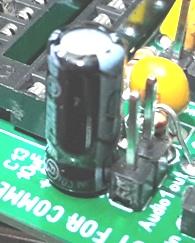
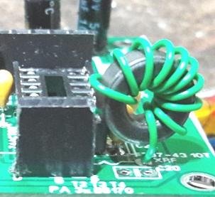
35. Montando soquete do PA
Usamos soquete pois o PA pode queimar e fica dificil trocar os
transistores.
35. Mounting the PA socket
We use socket because the PA can burn and it is difficult to change the
transistors.
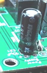
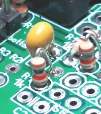
36. Montando C13 10µF.
Acoplamento de sinais de baixa frequencia. Cuidado com a polaridade !
36. Mounting C13 10µF.
Coupling of low frequency signals. Watch out for polarity!
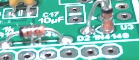
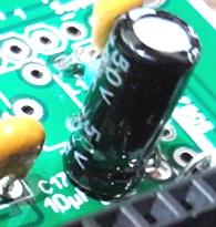
37 Montando C17 10µF.
Filtro de 5V CC.
37 Mounting C17 10µF.
5V DC filter.
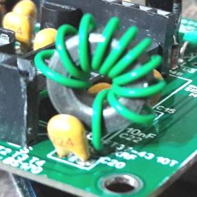
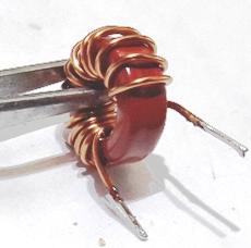
38. Montando choque de RF XRF 100µH.
Impede a passagem de RF do Pa para a fonte e deixa passar a corrente ad
fonte para o PA.
38. Mounting XRF 100µH RF shock.
It prevents the passage of RF from the Pa to the source and lets the
current from ad source to the PA.
Enrolando 10 espiras de fio telefonico isolado, cada passagem pelo furo
conta uma espira, caso o fio não tenha isolação
plastica, o furo do toroide deve ser lixado para reirar rebarbas que
possam danificar o esmalte do fio.
Winding 10 turns of insulated telephone wire, each passage through the
hole counts one turn, if the wire does not have plastic insulation, the
hole in the toroid must be sanded to remove burrs that could damage the
enamel of the wire.
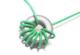
O choque fica ao lado do PA como na foto.
The shock is next to the PA as in the photo.
39. Soldando C20 de 220nF (224).
Tem a função de eliminar RF na linha de
alimentação.
39. Welding C20 from 220nF (224).
It has the function of eliminating RF in the power line.
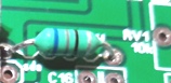
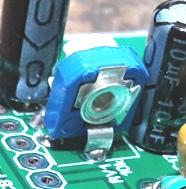
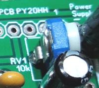
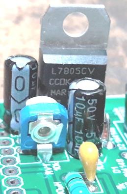
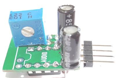
40. Trimpot RV1 10k.
Tem a função de controlar o brilho do LCD.
A regulagem fica quase toda a direita (horario).
40. Trimpot RV1 10k.
It has the function of controlling the LCD brightness.
The adjustment is almost all the way to the right (time).

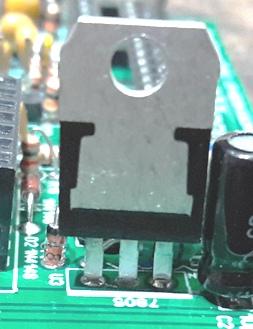
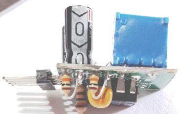
41. Montagem do regulador 7805
41. Assembly of the 7805 regulator
42. Ligando a alimentação
42.
Ligando a alimentação
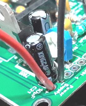
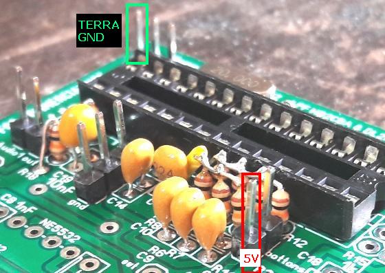
43. Alimentando e conferindo tensões.
43. Feeding and checking voltages.
Meça com um multimetro a tensão 5V nos pontos marcados :
Atmega 328 pinos 7, 18 e 20 ...nos pinos 27 e 28 a tensão
será ligeiramente menor.
74ACT00 pino 14
74HC4053 pino 16
NE5532 pino 8
Measure the 5V voltage at the marked points with a multimeter:
Atmega 328 pins 7, 18 and 20 ...on pins 27 and 28 the voltage will be
slightly lower.
74ACT00 pin 14
74HC4053 pin 16
NE5532 pin 8
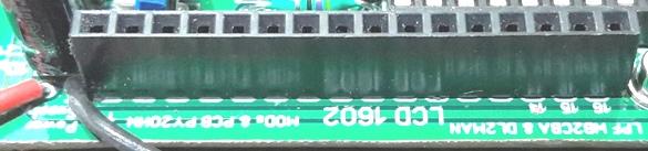
44. Solde o conector do LCD.
A conecção do LCD poderá ser feita com fios
soldados diretamente, ou com conector.
Já o conector pode ser soldado
44. Solder the LCD connector.
The LCD connection can be made with soldered wires directly, or with a
connector.
The connector can be soldered
na frente ..a PCB ficará na horizontal.
in front ..the PCB will be horizontal.
Soldado
Solded
ou atrás com montagem vertical da PCB ..optamos por esta
or behind with vertical PCB mounting ..we opted for this
Foto da soldagem
Solder photo
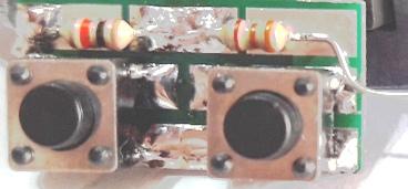
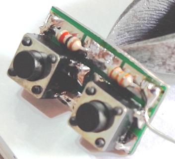
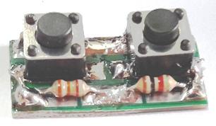
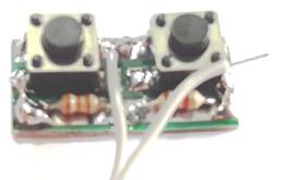
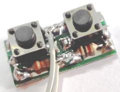
45. Montando os controles de painel : as chaves.
45. Assembling the panel controls : the switches.
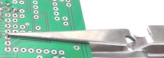
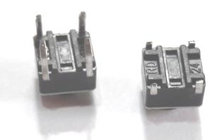
cortar a pcb das chaves
cut the keys pcb
Com um alicate de bico, juntar as quatro conexões junto ao corpo
da chave (a direita a feita).
With needle-nose pliers, join the four connections next to the key body
(the one made on the right).
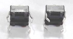
Cortar com rente os lides
Cut the edges close
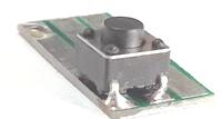
Posicionar na PCB as duas chaves
Position the two switches on the PCB
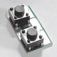
Solde a chave cuidando para que fique alinhada e preste
atenção para não soldar errado, a
posição é como esta nas fotos
Solder the key taking care that it is aligned and pay attention not to
solder wrong, the position is as shown in the photos
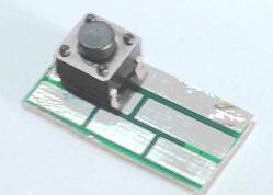
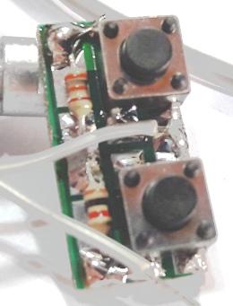
Soldando R20 1K
Os resistores das chaves permitem que o Atmega, por uma entrada
apenas, saiba qual da tres chaves esta acionada, por um divisor
de tensão formado pelos resistores.
Welding R20 1K
The resistors of the switches allow the Atmega, by a single input, to
know which of the three switches is activated, by a voltage divider
formed by the resistors.
O resistor que ficará a direita do painel é o de 1k.
The resistor that will be on the right of the panel is the 1k resistor.
O lide do resistor deve ser conectado a chave e soldado
The resistor lead must be connected to the switch and soldered
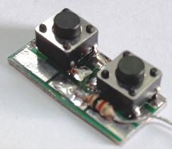
As chaves montadas
The assembled keys
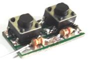
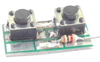
Montando o resistor R19 de 3k3
Assembling the 3k3 resistor R19
Plaquinha montada
plate mounted
Ligações da placa das chaves
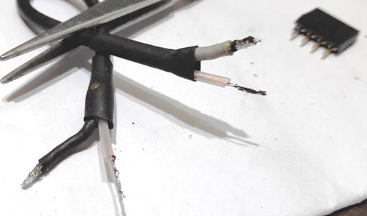
Separar e cortar 2 fios do flat cable de 10 cm.
Retirar a capa plastica e pré estanhar.
key board connections
Separate and cut 2 strands of the 10 cm flat cable.
Remove the plastic cover and pre-tin.
Soldar um fio conforme a foto
Solder a wire as shown in the photo
Soldar outro fio cuidando para que fiquem do comprimento correto.
Solder another wire making sure they are the correct length.
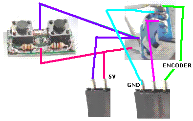
Conector de 3 fios do encoder... 3 fios do flat cable com cerca de 10 a
15cm..usei a propria placa para facilitar a solagem, pois o conector
fica fixo. Usei espaguetes encolhiveis..
3-wire encoder connector... 3-wire flat cable with about 10 to 15cm..I
used the board itself to facilitate the soldering, as the connector is
fixed. I used heat shrinkable spaghetti.
Montando o conector de dois fios dos botões - chaves
Solde
dois fios retrados do
flat cable com cerca de 15cm (maior que 10cm), a um terminal femea de
dois pinos. Esqueci dos espaguetes encolhiveis SRY. Proteja com
espaguetes e identifique um lado do fio nas duas pontas. Ao retirar a
capa dos fios do flat cable procure unir os fios multiplos de cada
cabinho e pré solde,
Assembling the two-wire connector of the buttons - switches
Solder two wires retracted from the flat cable with about 15cm (larger
than 10cm) to a two-pin female terminal. I forgot the SRY Shrinkable
Spaghetti. Protect with spaghetti and identify one side of the wire at
both ends. When removing the cover of the flat cable wires, try to
unite the multiple wires of each cable and pre-sold,
Identifique um dos fios nas duas pontas
Identify one of the wires at both ends
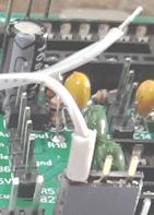
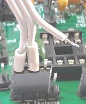
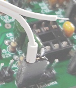
Montando o cabo de 3 fios no encoder.
"ATENÇÂO o fio que liguei esta errado, nas fotos segintes,
deverá ser
ligado ao terminal direito e não esquerdo do encoder ". Use
o croquis para se orientar melhor.
O fio marcado com preto é o fio terra e será soldado ao
pino central do encoder e em uma daslaterais do conector que vai ligado
a PCB.
Assembling the 3-wire cable on the encoder.
"ATTENTION the wire I connected is wrong, in the following photos, it
must be connected to the right and not the left terminal of the
encoder". Use the sketch to orient yourself better.
The wire marked with black is the ground wire and will be soldered to
the central pin of the encoder and to one of the sides of the connector
that is connected to the PCB.
Para ajudar a fixação use um lide de componente
To help fixing use a component lead
Como devem ser ligados e interligados o encoder as chaves e os
conectores
How the encoder, switches and connectors should be connected and
interconnected
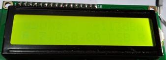
46. Ligando e ajustando o LCD.
Para ligar o LCD devemo plugar o ATMEGA328 e o LCD (observar pino 1 dos
dois), ligar a alimentação ...
Caso 1 tudo escuro ajuste para clarear pelo trimpot RV1,
até aparecer o display com letras
46. Turning on and adjusting the LCD.
To turn on the LCD we must plug the ATMEGA328 and the LCD (observe pin
1 of the two), turn on the power ...
Case 1 everything is dark, adjust to lighten through the RV1 trimpot,
until the display with letters appears
Caso 2 tudo branco ajuste RV1 até obter o display com
letras
Case 2 all white adjust RV1 until you get the display with letters
Caso 3 Ajustado !
falta foto
Case 3 Adjusted !
missing photo
XXXXXXXXXXXXXXXXXXXXXXXXXXXXXXXXXXXXXXXX
Parte B MENU
Para receber ou transmitir ou ajustar é necessário
conhecer o menu e as funções das chaves de comando do
encoder.
Os comandos são
Chave direita (conectada ao resistor de 1k)
Chave esquerda (conectada ao resistor de 3k3)
Chave do encoder (acionada pressionando o eixo do encoder para baixo).
Encoder (girando horario ou anti horario).
Part B MENU
To receive or transmit or adjust it is necessary to know the menu and
the functions of the encoder command switches.
The commands are
Right switch (connected to 1k resistor)
Left switch (connected to 3k3 resistor)
Encoder switch (activated by pressing down on the encoder shaft).
Encoder (rotating clockwise or counterclockwise).
Função do encoder
Chave do encoder
1 (um) pulso rapido : altera o cursor para baixo.
1 (um) pulso longo : altera o cursor para cima.
2 (dois) pulsos rapidos : altera a banda para cima (default de 80 a 10m)
Pressionando a chave e girando o encoder ao mesmo tempo aumentamos ou
dimuimos o volume de audio.
Encoder altera frequencia ou valores do menu quando selecionado .
Função da chave direita
1(um) pulso rapido muda de modo basico (LSB, USB e CW).
1 (um) pulso longo aciona o modo RIT ajuste o valor pelo encoder e
retorne apertando o botão novamente.
2 (dois) Pulsos rapidos aciona o filtro de audio, alterando a cada vez
que acionamos duas vezes.
Para SSB : BW = full ou sem filtros, 3kHz, 2,8kHz e 1,8kHz
Para CW : BW = 500Hz, 200Hz, 100Hz, 50Hz
2 (dois) pulsos longos altera o VFO de A para B ou vice versa.
Função da chave esquerda
1 pulso qualquer aciona o MENU
encoder function
encoder key
1 (one) fast pulse : changes the cursor down.
1 (one) long pulse : changes the cursor up.
2 (two) fast pulses : changes the band up (default from 80 to 10m)
Pressing the switch and turning the encoder at the same time increases
or decreases the audio volume.
Encoder changes frequency or menu values when selected.
Right key function
1 (one) fast pulse switches basic mode (LSB, USB and CW).
1 (one) long pulse activates the RIT mode, adjust the value through the
encoder and return by pressing the button again.
2 (two) Fast pulses triggers the audio filter, changing each time we
trigger it twice.
For SSB : BW = full or unfiltered, 3kHz, 2.8kHz and 1.8kHz
For CW : BW = 500Hz, 200Hz, 100Hz, 50Hz
2 (two) long pulses changes the VFO from A to B or vice versa.
Left key function
1 pulse any triggers the MENU
Menu :
Para alterar o valor do menu selecionado 1 (um) pulso da chave esquerda
novamente e altere girando o encoder. Para retornar ao menu acione a
chave direita ou esquerda, para voltar ao display acione outra vez uma
das chaves. Importante em qulquer seleção do menu o
ajuste pode ser observado em tempo real (sem voltar ao display).
Seleção :
1.1 Volume ( valores de -1 a +16 )
1.2 Modo (valores LSB, USB, CW, FM e AM)
1.3 Filtro valores
Para SSB
: BW = full ou sem filtros, 3kHz, 2,8kHz e 1,8kHz
Para CW : BW = 500Hz, 200Hz, 100Hz, 50Hz
1.4 Banda (valores 160m, 80m, 60m, 40m, 30m, 20m, 17m, 15m,12m, 10m e
6m)
1.5 Turn rate (razão de sintonia) valores: 1, 10, 100, 500, 1K,
10k, 100k, 500k, 1M, 10M)
(Veja é possivel alterar 1Hz , mas não é mostrado
no display, somente ao atingir 10Hz ou menos que 0).
para sair
do MENU é só acionar a chave direita
1.6 VFO mode valores : A ou B
1.7 RIT valores: ON ou OFF
1.8 AGC valores: Slow, Fast, Off
1.9 NR redutor de ruidos valores de 0 a 8
1.10 ATT atenuação 1 valores em dB: 0, -13, -20, -33,
-40, -53, -60 e -73.
1.11 ATT 2 atenuação 2 valores : 0 a 16
1.12 Smeter valores: Off, dBm, S, s-bar e wpm
2.1 CW decoder valores: On Off
2.4 Seni QSK valores : On Off
2.5 Keyer Speed valores em WPM : 1 a 60
2.6 Keyer mode valores: Straight (pica pau), iambico B, iambico A
2.7 Keyer swap valores Off On
2.8 Pratice valores On Off
3.1 Vox valores ON OFF
3.2 Noise Gate valores 0 a 255
3.3 TX Drive valores: 0 a 8
8.1 PA Bias min. valores 0 a 255
8.2 PA Bias max. valores 0 a 255
8.3 REF. Freq. valor: 25000000 (varia de 1 em 1 Hz ajusta a frequencia
exata do radio)
8.4 IQ Phase valor: 90 (varia de 1 em 1 grau).
10.1 Back ligth valores On Off
Menu:
To change the value of the selected menu 1 (one) pulse of the left key
again and change it by turning the encoder. To return to the menu,
press the right or left key, to return to the display, press one of the
keys again. Important in any menu selection, the adjustment can be
observed in real time (without returning to the display).
Selection:
1.1 Volume (values from -1 to +16)
1.2 Mode (LSB, USB, CW, FM and AM values)
1.3 Filter values
For SSB : BW = full or unfiltered, 3kHz, 2.8kHz and 1.8kHz
For CW : BW = 500Hz, 200Hz, 100Hz, 50Hz
1.4 Band (values 160m, 80m, 60m, 40m, 30m, 20m, 17m, 15m, 12m, 10m
and 6m)
1.5 Turn rate (tuning ratio) values: 1, 10, 100, 500, 1K, 10k, 100k,
500k, 1M, 10M)
(See it is possible to change 1Hz , but it is not shown on the display,
only when reaching 10Hz or less than 0).
to exit the MENU just press the right key
1.6 VFO mode values : A or B
1.7 RIT values: ON or OFF
1.8 AGC values: Slow, Fast, Off
1.9 NR noise reducer values from 0 to 8
1.10 ATT attenuation 1 values in dB: 0, -13, -20, -33, -40, -53, -60
and -73.
1.11 ATT 2 attenuation 2 values: 0 to 16
1.12 Smeter values: Off, dBm, S, s-bar and wpm
2.1 CW decoder values: On Off
2.4 Seni QSK values : On Off
2.5 Keyer Speed values in WPM: 1 to 60
2.6 Keyer mode values: Straight (woodpecker), iambic B, iambic A
2.7 Keyer swap values Off On
2.8 Practice On Off values
3.1 Vox ON OFF values
3.2 Noise Gate values 0 to 255
3.3 TX Drive values: 0 to 8
8.1 PA Bias min. values 0 to 255
8.2 AP Bias max. values 0 to 255
8.3 REF. Freq. value: 25000000 (varies from 1 to 1 Hz adjusts the exact
frequency of the radio)
8.4 IQ Phase value: 90 (varies from 1 to 1 degree).
10.1 Back light values On Off
xxxxxxxxxxxxxxxxxxxxxxxxxxxxxxxxxxxxxxxxxx
47. Soldando o modulo SI5351
Solde o conector fornecido com o modulo, cuidando para que fique em 90
graus.
47. Welding the SI5351 module
Solder the connector supplied with the module, making sure it is at 90
degrees.
48.Testando as funções do encoder e chaves.
Vamos conectar os CIs, o display e o encoder/chaves. Os Cis devem ser
colocados com o pino1 no lugar certo.
O encoder deve ser ligado
observando a marcação de terra.
48.Testing the encoder and switches functions.
Let's connect the ICs, the display and the encoder/switches. The Cis
must be placed with pin1 in the right place.
The encoder must be connected observing the ground marking.
Chaves a
marcação de 5V.
Keys marking 5V.
Costumo marcar os conectores com esmalte para unhas de cores diferentes
para
identificar as ligações corretas.
Falta a Foto
I often mark the connectors with different colored nail polish to
identify the correct connections.
Photo is missing
49. Teste o encoder as chaves ..pratique algumas
alterações conforme explicado no menu...
49. Test the encoder keys ..practice some changes as explained in the
menu...
50. Vamos corujar os 40m...
Para isto vamos soldar um jumper para anular o amplificador de RF, que
nesta banda satura a recepção.
Montar o LPF
Montar o jack de fone/auto falante
Montar um jack para antena
50. Let's listen to the 40m...
For this we are going to solder a jumper to cancel the RF amplifier,
which in this band saturates the reception.
Mount the LPF
Assemble the headphone/speaker jack
Mount an antenna jack
51. Jumper do amplificador de RF.
foto faltante
51. RF amplifier jumper.
missing photo
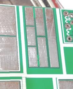
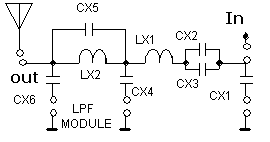
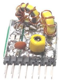
52. Montando o LPF.
O esquema dos filtros passa baixas (LPF)
52. Mounting the LPF.
The scheme of low pass filters (LPF)
A montagem da PCB do filtro
Assembling the filter PCB
 outra foto
Valores dos elementos dos filtros por banda
Values of filter elements per band
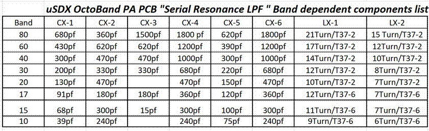
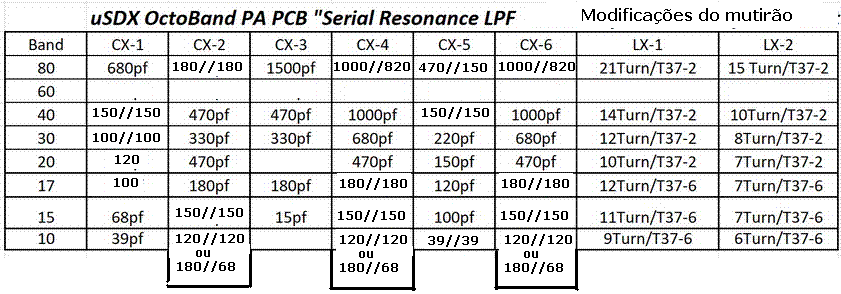
Devido a falta de valores corretos, substituimos alguns :
Due to lack of correct values, we substituted some :
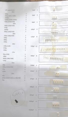
Os capacitores do KIT foram fornecidos em uma folha de papel
colados com fita
adesiva.
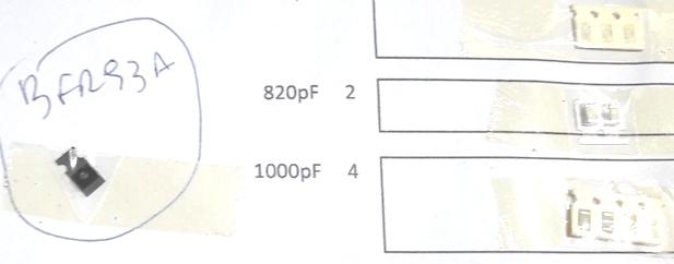
Atenção o transistor amplificador de RF BFR93 que
é SMD esta tambem colado nesta folha !
The KIT capacitors were supplied on a sheet of paper glued with
adhesive tape.
Attention the RF amplifier transistor BFR93 which is SMD is also pasted
on this sheet!
53. LPF 40m
Cortada a PCB solde os terminais (8) na placa.
Para soldar apoie o conector em outra placa com a mesma espessura.
Posicione o conector mantendo os pinos conforme foto
53. LFP 40m
Cut the PCB and solder the terminals (8) to the board.
To solder, support the connector on another plate of the same thickness.
Position the connector keeping the pins as shown in the photo
solde um pino e verifique se esta tudo em ordem
solder a pin and check if everything is in order
Solde os demais pinos
Solder the other pins
Separe CX1 2x 150pF (não separe mais para não misturar).
Solde CX1
separate CX1 2x 150pF (do not separate further to avoid mixing).
CX1 solder
Separe CX2 e CX3 de 470pF
Solde CX2 e CX3
Separate CX2 and CX3 from 470pF
Solder CX2 and CX3
Separe CX4 1000pF
Solde CX4
Separate CX4 1000pF
CX4 solder
Separe CX5 2x 150pF
Solde CX5
Separate CX5 2x 150pF
CX5 solder
Separe CX6
Solde CX6
Separate CX6
CX6 solder
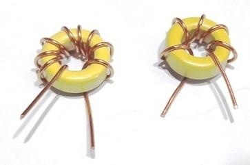
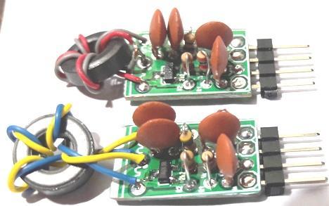
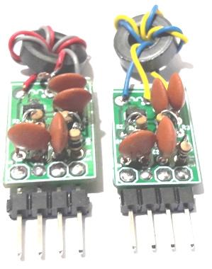
Toroides
Usaremos 2 toroides T37-2 (vermelho)
LX1 14 Voltas (cada vez que o fio passa lelo furo contamos uma volta).
Pelo mini ring core .. 14 voltas usa 16cm de fio ...adicionei 3cm para
conexões, usei 19cm.
Depois de enrolada, o fio enviado é soldavel ou seja o verniz
dele sai com o calor, usei minha pinça travante para soldar.
toroids
We will use 2 T37-2 toroids (red)
LX1 14 Turns (each time the thread passes through the hole we count one
turn).
For the mini ring core .. 14 turns uses 16cm of wire ...I added 3cm for
connections, I used 19cm.
After being wound, the wire sent is solderable, that is, the varnish
comes off with the heat, I used my locking tweezers to solder.
LX2 10 Voltas
LX2 10 turns
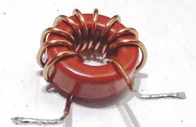
Solde LX1
Solder LX1
Solde LX2
Solder LX2

Observação outros modulos de LPF devem seguir o mesmo
procedimento.
Note other LPF modules must follow the same procedure.
54. Cabo de saida de audio
Use o plug mono !
54. Audio output cable
Use the mono plug!
No conector usei espagueti encolhivel, desculpe mas não foi no
kit !:(
In the connector I used shrinkable spaghetti, sorry but it wasn't in
the kit !:(
55. Cabo / conector de antena.
Use o cabo coaxial e o conector BNC fornecido, o BNC pode ser
substituido por um conector UHF ou um conector femea RCA.
55. Cable / Antenna Connector.
Use the coaxial cable and the BNC connector provided, the BNC can be
replaced with a UHF connector or an RCA female connector.
Para teste soldamos o BNC sem o painel
For testing we soldered the BNC without the panel
Agora podemos corujar os 40 e 80m ...
Coloque os CIs, o Display, o modulo SI5351, o modulo LPF , o encoder
com as chaves.
Conector de antena ...ligue a antena
Ligue os 12V
conecte um fone ou auto falante pequeno..
Aviso : devido a baixa impedancia de alguns fones / falantes pode
acontecer do Atmega reiniciar ao ligar e não funcionar ..
desconectando o fone / falante o Atmega volta a fucionar normalmente.
Now we can owl the 40 and 80m...
Place the ICs, the Display, the SI5351 module, the LPF module, the
encoder with the keys.
Antenna connector ...connect the antenna
Turn on the 12V
plug in a headphone or small speaker..
Warning: due to the low impedance of some headphones/speakers it may
happen that the Atmega restarts at power on and does not work ..
unplugging the headphones/speaker the Atmega works normally again.
xxxxxxxxxxxxxxxxxxxxxxxxxxxxxxxxxxxxxxxxxxxxx
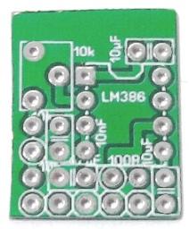
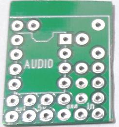
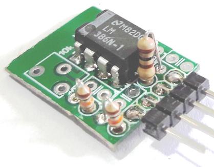
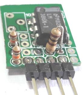
Modulo amplificador de audio.
Vamos cortar a placa PCB
Audio amplifier module.
Let's cut the PCB board
Corte um conector macho com 4 pinos e posicione como na foto
Cut a 4-pin male connector and position it as in the photo
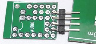
Solde 1 pino e depois se tudo certo solde os outros pinos
Solder 1 pin and then if everything is ok solder the other pins
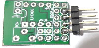
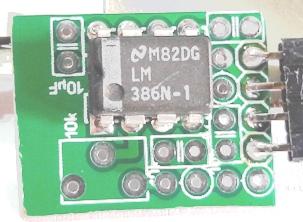
Aqui mais uma mancada do macanudo ... não inclui no kit outro
soquete de 8 pinos, solde o LM386 diretamente, cuidando para o pino
estar no lugar certo
Here's another blunder from the macanudo ... another 8-pin socket is
not included in the kit, solder the LM386 directly, taking care that
the pin is in the right place
Soldando R21 (10k)
R21 R22 e C23 formam um filtro para o PWM do Atmega, deixando passa
frequencias abaixo de 10kHz (audio).
Solder R21 (10k)
R21 R22 and C23 form a filter for the Atmega's PWM, allowing
frequencies below 10kHz (audio) to pass.
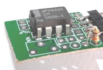
Soldando R22
Solder R22
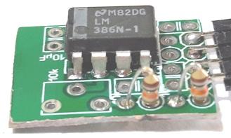
Soldando R23
Solder R23
R23 limita a corrente (e potencia / consumo) do LM386.
R23 limits the current (and power / consumption) of the LM386.
Soldando C23 (10nF ou 103)
Solder
C23 (10nF or 103)
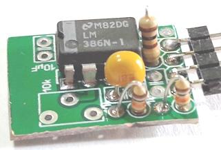
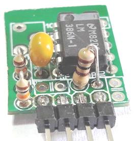
Soldado C25 10µF
Solder
C25 10µF
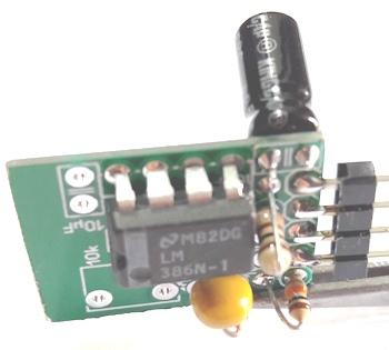
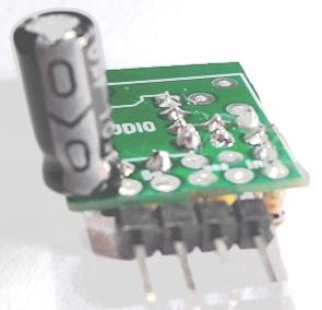
Soldando C24 10µF ... no esquema 47µF (sem problemas devido
a baixa corrente).
C24 ajuda a manter a corrente do LM386 estavel.
Soldering C24 10µF ... in the 47µF scheme (no problems due
to low current).
C24 helps keep the LM386's current steady.
Soldando o trimpot RV2 de 10k
RV2 controla o volume do audio ... ajuste ele em função
do controle de volume do software.
Sem distorção ..
Welding the 10k RV2 trimpot
RV2 controls the audio volume... adjust it according to the software's
volume control.
No distortion..
Agora fica melhor para corujar ...
Now it's better to listen...
XXXXXXXXXXXXXXXXXXXXXXXXXXXXX
Vamos ao TX
Montagem do conector de microfone
Precisaremos de:
Um cabinho de 3 fios (do flat cable) com 12cm ou mais.
Conector femea com 3 pinos
Jack ou plug estereo
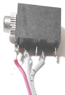
Soldando
Fios da esquera para a direita nas fotos 1. Terra (PTT e microfone)
2. Microfone 3. PTT
let's go to TX
Microphone jack assembly
We will need:
A 3-wire cable (from the flat cable) measuring 12cm or more.
3 pin female connector
stereo jack or plug
soldering
Wires from left to right in photos 1. Ground (PTT and microphone) 2.
Microphone 3. PTT
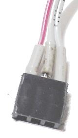
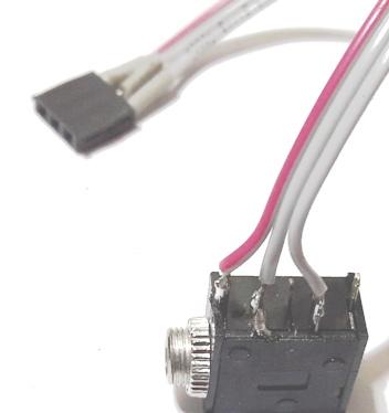
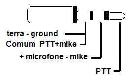
Ligações do plug do microfone com jack ou plug P2
Microphone plug connections with jack or P2 plug
Como fazer um microfone simples e
barato
How to make a simple and cheap microphone
Agora podemos testar o TX ....
NÃO É NECESSARIO O PA ...alias sem o PA.
Precisaremos do cabo de microfone, do microfone com plug, do USDX
montado e de um receptor (SSB) pode ser 40m ou 80m.
Plugar o microfone
Ligar o USDX em12V
Colocar o USDX na frequencia desejada e no modo LSB
Ligar o Receptor (com uma antena ou rabicho de fio) na mesma frequencia
do USDX em LSB.
Apertar o PTT e fale ao microfone ... ajuste a frequencia do RX para
acertar a inteligibilidade ...
Mude para USB ... CW em CW vc tem sinal apertando o PTT ( o USDX
esta como manipulador pica pau se vc não mudou no menu)
Confira a rejeição : estando em LSB tente ouvir USB e
vice versa
Now we can test the TX....
THE PA IS NOT NECESSARY ...alias without the PA.
We will need the microphone cable, the microphone with plug, the
mounted USDX and a receiver (SSB) it can be 40m or 80m.
plug the microphone
Connect the USDX to 12V
Put the USDX on the desired frequency and in LSB mode
Connect the Receiver (with an antenna or pigtail) to the same frequency
as the USDX on LSB.
Press PTT and speak into the microphone...adjust the RX frequency to
get the intelligibility right...
Change to USB ... CW to CW you have a signal by pressing the PTT (USDX
is as a woodpecker handler if you haven't changed in the menu)
Check out the rejection: being on LSB try listening to USB and vice
versa
XXXXXXXXXXXXXXXXXXXXXXXXXXXXXXXXXXX
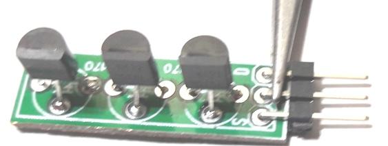
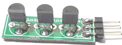
Montando o PA (amplificador de potencia).
Precisaremos
PCB do PA com BS170 corte da PCB principal
3 transistores BS170
Terminal ou conector macho com 3 pinos
Solde os transistores, observe nas fotos a posição
correta dos lides.
Nota o 2N7000 tem as conexões de supridouro e dreno invertidas
...existem transistores BS170 falsos que a ligação esta
como dos 2N7000 e ao ligar queimam ..são 2N7000
remarcados.
Assembling the PA (power amplifier).
we will need
PA PCB with BS170 main PCB cut
3 BS170 transistors
3-pin male terminal or connector
Solder the transistors, observe in the photos the correct position of
the leads.
Note the 2N7000 has the supply and drain connections inverted ...there
are false BS170 transistors that the connection is like the 2N7000 and
when they are turned on they burn ..there are 2N7000 rescheduled.
Para soldar os terminais usei a pinça que ajuda travando
mecanicamente o conector
To solder the terminals I used the tweezers that help mechanically
locking the connector
xxxxxxxxxxxxxxxxxxxxxxxxxxxxxxxxxxxxxxxxx
Ajustando a frequencia exata Recepção e
transmissão.
É possivel via menu ajustar a frequencia com precisão, o
ajuste que fiz foi de ouvido acertando o timbre do SSB e a frequencia
em 0 ou 5 kHz ... exemplo colega transmitindo em 7080 kHz ou em
7095 kHz.
O ideal seria com um frequecimetro de alta precisão medir a
frequencia do clock do modulo SI5351n então acertar a REF do
USDX.
Caso aja necessidade de maior precisão devemos :
1. Ir ao menu pulsando o botão esquerdo.
2 Navegue girando o encoder até 8.3
8.3 REF.
Freq. valor: 25000000 (varia de 1 em 1 Hz ajusta a frequencia
exata do radio)
O valor que coloquei foi 25003000Hz que é bem proximo do exato e
é valido para os modulos SI5351 comprados na China.
3. Aperte novamente o botão esquerdo habilitando a
mudança (aparece o sinal ">" no display)
4. Varie a frequencia de referencia para cima ou para baixo, de um em
um Hz, ( durante a variação o RX muda automaticamente, ao
sair ele altera o valor de Referencia) até que atinja o valor
pretendido.
5. Aperte novamente o botão esquerdo para gravar e sair.
Adjusting the exact frequency Receive and transmit.
It is possible via the menu to adjust the frequency precisely, the
adjustment I made was by ear setting the SSB timbre and the frequency
at 0 or 5 kHz ... example colleague transmitting at 7080 kHz or 7095
kHz.
The ideal would be with a high-precision frequency meter to measure the
clock frequency of the SI5351n module then set the USDX REF.
If there is a need for greater precision, we should:
1. Go to the menu by pressing the left button.
2 Navigate by turning the encoder to 8.3
8.3 REF. Freq. value: 25000000 (varies from 1 to 1 Hz adjusts the exact
frequency of the radio)
The value I put was 25003000Hz which is very close to the exact one and
is valid for SI5351 modules bought in China.
3. Press the left button again to enable the change (the ">" sign
appears on the display)
4. Vary the reference frequency up or down, one by one Hz, (during the
variation, the RX changes automatically, when exiting it changes the
Reference value) until it reaches the desired value.
5. Press the left button again to record and exit.
XXXXXXXXXXXXXXXXXXXXXXXXXXXXXXXXXXXXXXXXXXX
Ajustes no TX
O Transmissor tem tres itens de ajuste no menu :
3.3 TX
Drive valores: 0 a 8
8.1 PA Bias min. valores 0 a 255
8.2 PA Bias max. valores 0 a 255
O item 3.3 TX Drive atual colocando uma tensão (AC) no gate do
PA, com um valor alto é possivel ter RF em SSB sem
modulação, o que não é correto. O valor
ajustado geralmente é entre 2 e 4.
8.1 Bias min é o valor minimo do Bias do gate do PA,
é um ajuste de corte do PA pelo valor mais baixo do Bias.
O valor ajustado geralmente é Zero. Este valor não
implica na potencia.
8.2 PA Bias max. é o ajuste mais importante do transmissor, ele
ajusta a tensão maxima do PA, deve ter o valor aumentado
até que a potencia para de subir, ou que a corrente atinja
valores perigosos para o PA. O valor para os BS170 geralmente é
de 130 a 150, para um IRF510 é de 255, já para o
IRLML2060 o valor é de 20 a 30.
Para ajustar o transmissor é preciso um amperimetro de 1A ou
mais, uma carga fantasma e um medidor de potencia.
No link explico algumas coisas
interessnates sobre como medir potencia de entrada e de saida
A carga fantasma pode ser 3 resistores de 150R 2W de metalfilme (6W),
ou uma carga fantasma (dummi load) comercial.
O medidor de potencia pode ser um diodo 1n4148 e um capacitor de 100nF
ligados como na explicação do IK3OIL no
SWR meter
TX settings
The Transmitter has three adjustment items in the menu:
3.3 TX Drive values: 0 to 8
8.1 PA Bias min. values 0 to 255
8.2 AP Bias max. values 0 to 255
The item 3.3 TX Drive current putting a voltage (AC) on the gate of the
PA, with a high value it is possible to have RF in SSB without
modulation, which is not correct. The adjusted value is usually between
2 and 4.
8.1 Bias min is the minimum value of the Bias of the gate of the PA, it
is an adjustment of the cut of the PA by the lowest value of the Bias.
The adjusted value is usually Zero. This value does not imply power.
8.2 AP Bias max. It is the most important adjustment of the
transmitter, it adjusts the maximum voltage of the PA, it must have the
value increased until the power stops rising, or the current reaches
dangerous values for the PA. The value for the BS170 is usually from
130 to 150, for an IRF510 it is 255, for the IRLML2060 the value is
from 20 to 30.
To adjust the transmitter you need an ammeter of 1A or more, a dummy
load and a power meter.
In the link I explain some interesting
things about how to measure input and output power (portuguese)
The dummy load can be 3
metalfilm (6W) 150R 2W resistors, or a commercial dummi load.
The power meter can be a 1n4148 diode and a 100nF capacitor connected
as in the explanation of IK3OIL
SWR meter
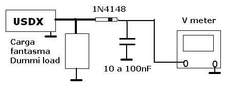
O valor da tensão medida deve ser acrescido de 0,7V devido ao
diosdo.
A corrente de entrada é medida com um amperimetro de 1 a 10A
colocado em serie com a alimentação poistiva do USDX.
Com os ajustes
3.3 TX
Drive 2
8.1 PA Bias min. 0
8.2 PA Bias max. valores 90
Coloque o PA, o LPF e conecte a carga fantasma ao terminal de antena.
Coloque o USDX em 7100kHz CW, aperte o PTT, verifcando a corrente de
entrada que deve ser aproximadamente 80 a 100 miliamperes em RX e
até 700mA em TX.
Correntes acima de 700mA exigem a diminuição do valor do
Bias Max.
A tensão de RF deve estar em 14 a 16V cerca de 3W.
The measured voltage value must be increased by 0.7V due to the diode.
The input current is measured with a 1 to 10A ammeter placed in series
with the positive supply of the USDX.
With the settings
3.3 TX Drive 2
8.1 PA Bias min. 0
8.2 AP Bias max. values 90
Put the PA, the LPF and connect the dummy load to the antenna terminal.
Set the USDX to 7100kHz CW, tighten the PTT, checking the input current
which should be approximately 80 to 100 milliamps in RX and up to 700mA
in TX.
Currents above 700mA require a decrease in the Bias Max value.
The RF voltage should be at 14 to 16V about 3W.
XXXXXXXXXXXXXXXXXXXXXXXXXXXXXXXXXXXXXXXXXXXXXXXXX
Ajustando o LPF
Com os ajustes de TX feitos e com correntes dentro dos limites.
Meça a potencia de 100 em 100kHz abrangendo o maior sinal ou
seja o maior sinal tem que estar dentro das medidas.
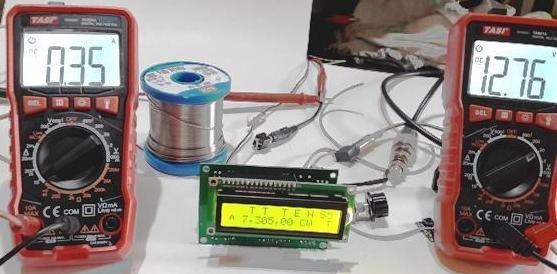
Como exemplo fiz medidas com o nosso USDX e o LPF de 40m montado
A esquerda corrnte em Ampere a direita tensao em Volts a pico Vp.
Adjusting the LPF
With TX adjustments made and currents within limits.
Measure the power from 100 to 100kHz covering the largest signal ie the
largest signal has to be within the measurements.
As an example I took measurements with our USDX and the 40m LPF mounted
Left current in Ampere right voltage in Volts at peak Vp.
7305 kHz
7200
7100
7005
6905
6805
6705
6605
6505
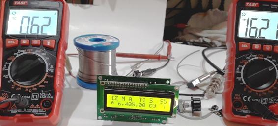
6405
6305
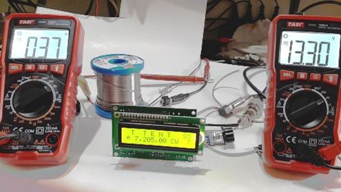
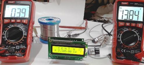
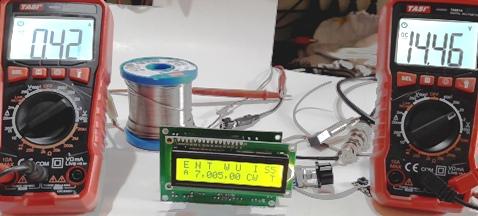
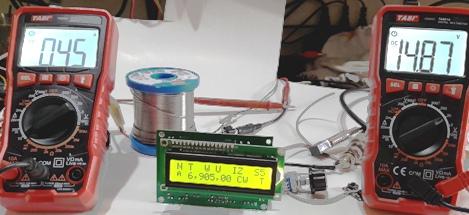
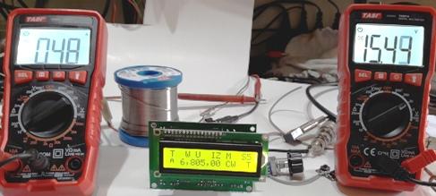
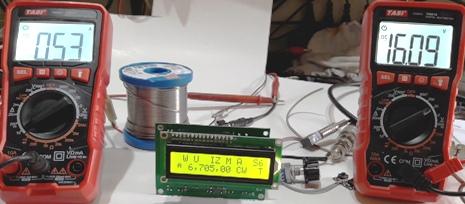
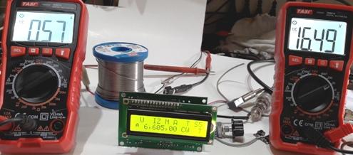
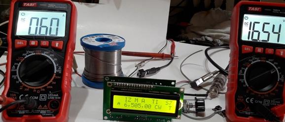
Tensões de RF (Vp) medidas (poderia ser em W)
RF voltages (Vp) measured (could be in W)
6300 15,62
6400 16,21
6500 16,54 <<=
6600 16,49 <<=
6700 16,09
6800 15,49
6900 14,87
7000 14,46
7100 13,84
7200 13,30
7300 12,76
Os valores maximos centrais estão em frequencias muito baixas, o
objetivo é de 7100 o valor central.
Para acertos pequenos, aqui em 40m da ordem de até 100kHz
é possivel ajustar comprimindo as espiras (para baixar a
frequencia) ou espaçar (para aumentar a frequencia.
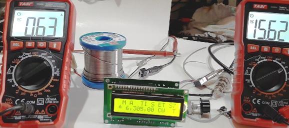
Neste caso estamos muito fora 600kHz, vou tirar duas espiras de LX2 (o
correto é retirar uma por vez), desenrolando de 10 para 8
espiras, sem cortar o fio (lembre-se o fio é soldavel não
precisa ser respado).
The maximum central values are at very low frequencies, the goal is
7100 the central value.
For small hits, here in 40m of the order of up to 100kHz it is possible
to adjust by compressing the turns (to lower the frequency) or spacing
(to increase the frequency.
In this case we are far outside 600kHz, I will take two turns from LX2
(the correct thing is to remove one at a time), unwinding from 10 to 8
turns, without cutting the wire (remember the wire is solderable and
does not need to be spared).
Retirei as espiras soldei, dobro o fio para não ter curto
circuito e medimos
Para ficar mais simples medi com um watimetro (acoplador) e a mesma
carga fantasma
Potencia em W
I removed the coils, soldered, doubled the wire so as not to have a
short circuit and we measured
To make it simpler, I measured it with a wattmeter (coupler) and the
same dummy load
power in W
6600 3,1
6700 3,2
6800 3,3
6900 3,3
7000 3,5
7100 3,6 <=
7200 3,7 <<=
7300 3,5
7400 3,4
Os valores estão dentro do esperado vamos soldar em definitivo e
cortar o fio.
The values are within the expected, we will definitely weld and cut the
wire.
O LPF esta pronto!
Vamos ajustar o bias maximo, ajustar a corrente e medir a potencia.
ajustes finais
Tensão de entrada 11,9V
Frequencia 7100khz
Ajustes
TX drive 2
PA bias min 0
PA bias max 110
Corrente em SSB sem falar (TX ON) 0,12A
Corrnte Total medida 0,69A
Corrente no PA 0,57A (0,69 - 0,12)
Potencia de entrada no PA 6,8W
Potencia de saida 5,2W
Rendimento 76% (5,2 * 100 / 6,8)
The LPF is ready!
Let's adjust the maximum bias, adjust the current and measure the power.
final adjustments
Input voltage 11.9V
Frequency 7100khz
Settings
TX drive 2
PA bias min 0
PA bias max 110
Current on SSB without talking (TX ON) 0.12A
Total current measured 0.69A
Current in the PA 0.57A (0.69 - 0.12)
Input power on the PA 6.8W
Output power 5.2W
Yield 76% (5.2 * 100 / 6.8)
XXXXXXXXXXXXXXXXXXXXXXXXXXXXXXXXXXX
LPF de 10m
Cortar a PCB do LPF 10m
Soldar terminais
10m LPF
Cut the LPF PCB 10m
solder terminals
Separe
CX1 39pF (não separe mais para não misturar).
Solde CX1
Separate CX1 39pF (do not separate further to avoid mixing).
CX1 solder
Separe CX2 e CX3 de 120pF (120pF paralelo com 120pF ou 180Pf paralelo
com 68pF)
Solde CX2 e CX3
Separate CX2 and CX3 from 120pF (120pF parallel with 120pF or 180Pf
parallel with 68pF)
Solder CX2 and CX3
Separe CX4 120pF (120pF paralelo com 120pF ou 180Pf paralelo
com 68pF)
Solde CX4
Separate CX4 120pF (120pF parallel with 120pF or 180Pf parallel with
68pF)
CX4 solder
Separe CX5 2x 39pF (paralelo)
Solde CX5
Separate CX5 2x 39pF (parallel)
CX5 solder
Separe CX6 120//120pF (ou 180pF paralelo com 68pF)
OBS. Depois dos ajustes ficou apenas um capacitor de 120pF e em
paralemo usei um trimer amarelo de 6-47pF...no caso de 180PF use
somente este capacitor. Na foto aparecem os dois, feita antes dos
ajustes
Solde CX6
Separate CX6 120//120pF (or 180pF parallel with 68pF)
NOTE After the adjustments there was only a 120pF capacitor and in
parallel I used a 6-47pF yellow trimer...in the case of 180PF use only
this capacitor. The photo shows both, made before the adjustments
CX6 solder
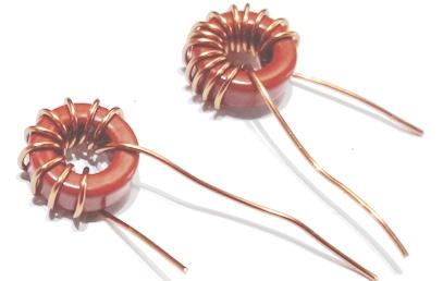
Toroides
Usaremos 2 toroides T37-6 (amarelo)
LX1 9 Voltas 243nH (cada vez que o fio passa pelo furo contamos
uma volta).
Pelo mini ring core .. 9 voltas usa 10cm de fio ...adicionei 3cm para
conexões, usei 13cm.
LX2 6
Voltas 108nH (cada vez que o fio passa pelo furo contamos uma
volta).
Pelo mini ring core .. 6 voltas usa 7cm de fio ...adicionei 3cm para
conexões, usei 10cm.
toroids
We will use 2 T37-6 toroids (yellow)
LX1 9 Turns 243nH (each time the wire passes through the hole we count
one turn).
For the mini ring core .. 9 turns uses 10cm of wire ... I added 3cm for
connections, I used 13cm.
LX2 6 Turns 108nH (each time the wire passes through the hole we count
one turn).
For the mini ring core .. 6 turns uses 7cm of wire ... I added 3cm for
connections, I used 10cm.
Após varios ajustes terminamos o LPF retirando um capacitor de
120pF e substituindo por um trimer amarelo de 6-47pF.
After several adjustments we finished the LPF by removing a 120pF
capacitor and replacing it with a 6-47pF yellow trimer.
Como perdi o capacitor de 39pF CX1 ... !:<( ... substitui por
um capacitor ceramico ...e soldei no terra o capacitor retirado para
não sumir ... detalhe na foto.
As I lost the 39pF CX1 capacitor ... !:<( ... replace it with a
ceramic capacitor ...and I soldered the removed capacitor to ground so
it wouldn't disappear ... detail in the photo.
Resultado 10m
3,2 W com 14,8V e 2,3W com 11,9V
Result 10m
3.2W at 14.8V and 2.3W at 11.9V
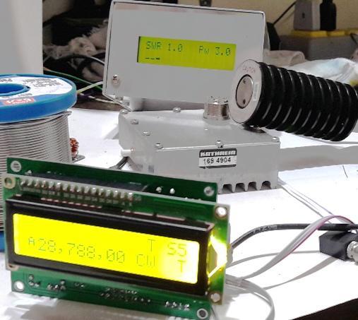
Ajustes
finais
Tensão de entrada 14,8V
Frequencia 28788khz
Ajustes
TX drive 2
PA bias min 0
PA bias max 110
Corrente em SSB sem falar (TX ON) 0,12A
Corrnte Total medida 0,41A
Corrente no PA 0,29A (0,41 - 0,12)
Potencia de entrada no PA 4.3W
Potencia de saida 3W ... 3,2W sem o amprimetro
Rendimento 70% (3 * 100 / 4.3) ...74% sem o amperimetro.
Final adjustments
Input voltage 14.8V
Frequency 28788khz
Settings
TX drive 2
PA bias min 0
PA bias max 110
Current on SSB without talking (TX ON) 0.12A
Total current measured 0.41A
Current in the PA 0.29A (0.41 - 0.12)
Input power on the PA 4.3W
Output power 3W ... 3.2W without the ammeter
Yield 70% (3 * 100 / 4.3) ...74% without the ammeter.
XXXXXXXXXXXXXXXXXXXXXXXXXXXXXXXXXXXXXXXX
Montagem do amplificador de RF (estou testando ele ....estou sem
antenas)
Cortar a placa.
Assembly of the RF amplifier (I'm testing it .... I'm out of antennas)
Cut the plate.
Onde esta o BFR93 no kit ?
Esta com os capacitores SMDs
Where is the BFR93 in the kit?
It has SMD capacitors
vamos soldar o BFR93 ... coloque solda em um ponto conforme foto :
vamos
soldar o BFR93 ... coloque solda em um ponto conforme foto :
Solde os outros terminais do transistor
Solder the other transistor terminals
Soldar R25 de 2k2 (marcado R2 na PCB).
Solder R25 from 2k2 (marked R2 on PCB).
Soldar R24 de 1k (marcado R1 na PCB).
Solder 1k R24 (marked R1 on PCB).
Soldar C27 100nF (marcado C1 na PCB).
Solder C27 100nF (marked C1 on PCB).
Soldar C30 100nF (marcado C2 na PCB).
Solder C30 100nF (marked C2 on PCB).
Soldar R27 de 10 Ohms (marcado R4 na PCB).
Solder R27 10 Ohms (marked R4 on PCB).
Soldar R26
de 47R (marcado R3 na PCB).
Solder R26 to 47R (marked R3 on PCB).
Soldar C28 100nF (marcado C3 na PCB).
(Os capacitores C28 e C29 podem ser soldados em duas
posições)
Solder C28 100nF (marked C3 on PCB).
(Capacitors C28 and C29 can be soldered in two positions)
Soldar C29 100nF (marcado C4 na PCB).
Solder C29 100nF (marked C4 on PCB).
Soldar conector macho de 4 pinos
Solder 4 pin male connector
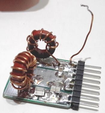
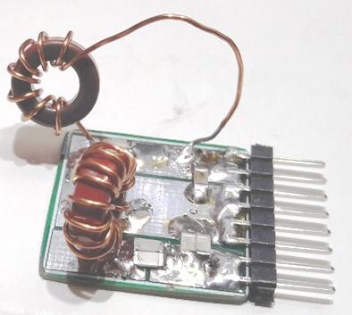
Montar a bobina (ou transformador bifilar)
Os dois fios trançados podem ser fios esmaltados, mas
identificados por cor ou por continuidade. este enrolamento tambem pode
ser feito com dois fios do flat cable.
Assemble the coil (or bifilar transformer)
The two stranded wires can be enameled wires, but identified by color
or continuity. this winding can also be done with two wires of the flat
cable.

Enrole 4 espiras no toroide, ligando o fim de um enrolamento com o
começo do outro.
Wind 4 turns on the toroid, connecting the end of one winding with the
beginning of the other.
Como ficaram dois amplificadores montados.
Note que C28 e C29 (proximos ao toroide) estão soldados em
posição diferentes.
How were two amplifiers assembled.
Note that C28 and C29 (next to the toroid) are welded in different
positions.
XXXXXXXXXXXXXXXXXXXXXXX
Muito cuidado ao testar sem caixa pois pode acontecer algum acidente !
Eu queimei nesta montagem um modulo SI5351 e um 74ACT00 .
O SI5351 queimado mostra um codigo no display tipo "BER_I2C=5000" que
alem do Si5351 queimado pode significar outras coisas.
Outros codigos podem aparecer mostrando que a tensão de 3.3V
esta com problemas e assim por diante.
Desconheço uma tabela e não tenho maiores
informações sobre este erros, mas posso ajudar, escreva
para meu email (esta na minha primeira pagina na WEB).
Be very careful when testing without a box because an accident can
happen!
I burned in this assembly a SI5351 module and a 74ACT00 .
The burnt SI5351 shows a code on the display like "BER_I2C=5000" which
in addition to the burnt Si5351 can mean other things.
Other codes may appear showing that the 3.3V voltage is faulty and so
on.
I don't know a table and I don't have more information about these
errors, but I can help, write to my email (this is on my first page on
the WEB).
XXXXXXXXXXXXXXXXXXXXXXX
Como eu carrego o software no ATMEGA.
Para carregar um software em um chip ATMEGA é necessario uma
ligação a porta USB do PC. Esta ligação
pode ser feita por um arduino UNO ou por um arduino Nano.
Observação importante : caso vc tenha um arduino UNO com
CHIP de 28 pinos, com bootloader
é só carregar o sketch diretamete nele usando a IDE do
arduino, trocando os chips do UNO com o novo . Caso não tenha o
bootloader é preciso seguir as instruções abaixo
para carregar o boot loader.
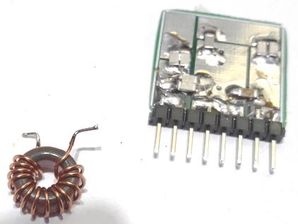
Materiais usados :
1. ATMEGA328P-PU com ou sem o bootloader
2. Arduino UNO ou Nano
3. Cabos
para ligar o UNO ou Nano ao PC via USB
4. PC pode ser com Windows 7 ou 10 ... com Windows XP somente com
arquivos tipo .HEX
5. Bred
board para o Atmega com mais de 28pinos
6. Cristal de 20MHz, resistor de 10k, conectores para
ligações.
No caso do USDX o criador do programa deixou disponivel até a
versão W, que é a ultima aberta.
Possibilidades de alteração de software (o que esta
configurado é o que temos no mutirão) :
para alterar, carregando o programa via arduino IDE 1.8.10 ou mais nova
( com Windows 7 ou 10) basta colocar ou retirar duas barras // antes de
"define".
How do I load the software on ATMEGA.
To load software on an ATMEGA chip it is necessary to connect it to the
PC's USB port. This connection can be made by an Arduino UNO or an
Arduino Nano.
Important note: if you have an Arduino UNO with a 28-pin CHIP, with the
bootloader just load the sketch directly into it using the Arduino IDE,
changing the UNO chips with the new one. If you don't have the
bootloader, you need to follow the instructions below to load the boot
loader.
Materials used:
1. ATMEGA328P-PU with or without bootloader
2. Arduino UNO or Nano
3. Cables to connect UNO or Nano to PC via USB
4. PC can be with Windows 7 or 10 ... with Windows XP only with .HEX
type files
5. Bred board for Atmega with 28+ pins
6. 20MHz crystal, 10k resistor, connectors for leads.
In the case of USDX, the creator of the program made available up to
the W version, which is the last open one.
Possibilities of software alteration (what is configured is what we
have in the task force):
to change, loading the program via arduino IDE 1.8.10 or newer (with
Windows 7 or 10) just put or remove two slashes // before "define".
Arduino IDE
download
Sketch ou programa .INO do USDX versão W
zipado
Arquivo .HEX do mutirão Usdx
versãoW
#define
VERSION "1.02w"
// Configuration switches; remove/add a double-slash at line-start to
enable/disable a feature; to save space disable e.g. CAT, DIAG, KEYER
#define
DIAG
1 // Hardware diagnostics on startup (only disable when
your rig is working)
#define
KEYER
1 // CW keyer
//#define
CAT
1 // CAT-interface
#define F_XTAL 27005000 // 27MHz SI5351
crystal
#define F_XTAL 25003000 // 25MHz SI5351 crystal
(enable for WB2CBA-uSDX, SI5351 break-out board or uSDXDuO)
//#define F_XTAL 25000000 // 25MHz SI5351
crystal (enable for 25MHz TCXO)
//#define SWAP_ROTARY 1 // Swap rotary
direction (enable for WB2CBA-uSDX)
//#define
QCX
1 // Supports older (non-SDR) QCX HW modifications (QCX,
QCX-SSB, QCX-DSP with I/Q alignment-feature)
//#define OLED_SSD1306 1 // OLED display
(SSD1306 128x32 or 128x64), connect SDA (PD2), SCL (PD3)
//#define OLED_SH1106 1 // OLED display
(SH1106 1.3" inch display), connect SDA (PD2), SCL (PD3), NOTE that
this display is pretty slow
//#define LCD_I2C
1 // LCD with I2C (PCF8574
module ), connect
SDA (PD2), SCL (PD3), NOTE that this display is pretty slow
//#define
LPF_SWITCHING_DL2MAN_USDX_REV3
1 // Enable 8-band filter bank
switching: latching relays wired to a
TCA/PCA9555 GPIO extender on the PC4/PC5 I2C bus; relays are using
IO0.0 as common (ground), IO1.0..7 used by the individual latches K0-7
switching respectively LPFs for 10m, 15m, 17m, 20m, 30m, 40m, 60m, 80m
//#define LPF_SWITCHING_DL2MAN_USDX_REV3_NOLATCH 1 //
Enable 8-band filter bank switching: non-latching relays wired to a
TCA/PCA9555 GPIO extender on the PC4/PC5 I2C bus; relays are using
IO0.0 as common (ground), IO1.0..7 used by the individual latches K0-7
switching respectively LPFs for 10m, 15m, 17m, 20m, 30m, 40m, 60m, 80m.
Enable this if you are using 8-band non-latching version for the
relays, the radio will draw extra 15mA current but will work ity any
relay (Tnx OH2UDS/TA7W Baris)
//#define
LPF_SWITCHING_DL2MAN_USDX_REV2
1 // Enable 5-band filter bank
switching: latching relays wired to a
TCA/PCA9555 GPIO extender on the PC4/PC5 I2C bus; relays are using
IO0.1 as common (ground), IO0.3, IO0.5, IO0.7, IO1.1, IO1.3 used by the
individual latches K1-5 switching respectively LPFs for 20m, 30m, 40m,
60m, 80m
//#define LPF_SWITCHING_DL2MAN_USDX_REV2_BETA
1 // Enable 5-band filter bank
switching: latching relays wired to a
PCA9539PW GPIO extender on the PC4/PC5 I2C bus; relays are
using IO0.1 as common (ground), IO0.3, IO0.5, IO0.7, IO1.1, IO1.3 used
by the individual latches K1-5 switching respectively LPFs for 20m,
30m, 40m, 60m, 80m
//#define
LPF_SWITCHING_DL2MAN_USDX_REV1
1 // Enable 3-band filter bank
switching: latching relays wired to a
PCA9536D GPIO extender on the PC4/PC5 I2C bus; relays
are using IO0 as common (ground), IO1-IO3 used by the individual
latches K1-3 switching respectively LPFs for 20m, 40m, 80m
#define LPF_SWITCHING_WB2CBA_USDX_OCTOBAND
1 // Enable 8-band filter bank switching: non-latching
relays wired to a MCP23008 GPIO extender on the
PC4/PC5 I2C bus; relays are using GND as common (ground), GP0..7 used
by the individual latches K1-8 switching respectively LPFs for 80m,
60m, 40m, 30m, 20m, 17m, 15m, 10m
//#define
LPF_SWITCHING_PE1DDA_USDXDUO
14 // Enable 2-band filter bank switching: non-latching
relay wired to pin PD5 (pin 11); specify as value the frequency
in MHz for which (and above) the relay should be altered (e.g. put 14
to enable the relay at 14MHz and above to use the 20m LPF).
#define SI5351_ADDR 0x60 // SI5351A I2C
address: 0x60 for SI5351A-B-GT, Si5351A-B04771-GT, MS5351M; 0x62 for
SI5351A-B-04486-GT; 0x6F for SI5351A-B02075-GT; see here for other
variants:
https://www.silabs.com/TimingUtility/timing-download-document.aspx?OPN=Si5351A-B02075-GT&OPNRevision=0&FileType=PublicAddendum
//#define F_MCU 16000000 // 16MHz ATMEGA328P
crystal (enable for unmodified Arduino Uno/Nano boards with 16MHz
crystal). You may change this value to any other crystal frequency (up
to 28MHz may work)
// Advanced configuration switches
//#define CONDENSED 1 //
Display in 4 line mode (for OLED and LCD2004 modules)
//#define CAT_EXT
1 // Extended CAT support: remote button and screen control
commands over CAT
//#define CAT_STREAMING 1 // Extended CAT support:
audio streaming over CAT, once enabled and triggered with CAT cmd,
samplerate 7812Hz, 8-bit unsigned audio is sent over UART. The ";" is
omited in the data-stream, and only sent to indicate the beginning and
end of a CAT cmd.
#define CW_DECODER 1 //
CW decoder
#define TX_ENABLE
1 // Disable this for RX only (no transmit), e.g. to
support uSDX for kids idea: https://groups.io/g/ucx/topic/81030243#6276
#define KEY_CLICK
1 // Reduce key clicks by envelope shaping
#define SEMI_QSK
1 // Just after keying the transmitter, keeps the RX muted
for a short amount of time in the anticipation for continued keying
#define RIT_ENABLE 1 //
Receive-In-Transit alternates the receiving frequency with an
user-defined offset to compensate for any necessary tuning needed on
receive
#define VOX_ENABLE 1 //
Voice-On-Xmit which is switching the transceiver into transmit as soon
audio is detected (above noise gate level)
//#define MOX_ENABLE 1 //
Monitor-On-Xmit which is audio monitoring on speaker during transmit
//#define FAST_AGC 1 //
Adds fast AGC option (good for CW)
//#define VSS_METER 1 //
Supports Vss measurement (as s-meter option), requires resistor of 1M
between 12V and pin 26 (PC3)
//#define SWR_METER 1 //
Supports SWR meter with bridge on A6/A7 (LQPF ATMEGA328P) by Alain,
K1FM, see: https://groups.io/g/ucx/message/6262 and
https://groups.io/g/ucx/message/6361
//#define ONEBUTTON 1 // Use
single (encoder) button to control full the rig; optionally use L/R
buttons to completely replace rotory encoder function
//#define DEBUG
1 // for development purposes only (adds debugging features
such as CPU, sample-rate measurement, additional parameters)
//#define TESTBENCH 1 //
Tests RX chain by injection of sine wave, measurements results are sent
over serial
//#define CW_FREQS_QRP 1 // Defaults to CW
QRP frequencies when changing bands
//#define CW_FREQS_FISTS 1 // Defaults to CW FISTS
frequencies when changing bands
//#define CW_MESSAGE 1
// Transmits pre-defined CW messages on-demand (left-click menu item
4.2)
//#define CW_MESSAGE_EXT 1 // Additional CW messages
//#define TX_DELAY 1 //
Enables a delay in the actual transmission to allow relay-switching to
be completed before the power is applied (see also NTX, PTX definitions
below for GPIO that can switch relay/PA)
//#define
NTX
11 // Enables LOW on TX, used as PTT out to enable external
PAs (a value of 11 means PB3 is used)
//#define
PTX
11 // Enables HIGH on TX, used as PTT out to enable external PAs
(a value of 11 means PB3 is used)
//#define CLOCK
1 // Enables clock
#define CW_INTERMEDIATE 1 // CW decoder shows
intermediate characters (only available for LCD and F_MCU at 20M),
sequences like: EIS[HV] EIUF EAW[JP] EARL TMO TMG[ZQ] TND[BX]
TNK[YC], may be good to learn CW; a full list of possible
sequences: EISH5 EISV3 EIUF EIUU2 EAWJ1 EAWP EARL TMOO0 TMOO9
TMOO8 TMGZ7 TMGQ TNDB6 TNDX TNKY TNKC
//#define F_XTAL 20000000 // Enable this for uSDXDuO,
20MHz SI5351 crystal
//#define TX_CLK0_CLK1 1 // Enable this for
uSDXDuO, i.e. when PA is driven by CLK0, CLK1 (not CLK2); NTX pin may
be used for enabling the TX path (this is like RX pin, except that RX
may also be used as attenuator)
//#define F_CLK2 12000000 // Enables a fixed CLK2
clock output of choice (only applicable when TX_CLK0_CLK1 is enabled),
e.g. for up-converter or to clock UART USB device
Hardware:
1.Gravando um ATMEGA328P-PU
Colocar o Atmega a ser gravado no bred board e conectar :
a. Cristal 20MHz ligado aos pinos 9 e 10
b. resistor de 10K entre pino 1 e o pino 7 (5V)
1.1 Com Arduino UNO
Atmega pinos 7 e 8 ligados ao pino 5V do Uno
Atmega pinos 8 e 22 ligados ao pino GND do Uno
Atmega pino 19 ligado ao pino 13 do Uno
Atmega
pino 18 ligado ao pino 12 do Uno
Atmega
pino 17 ligado ao pino 11 do Uno
Atmega
pino 1 ligado ao pino 10 do Uno
Hardware:
1.Writing an ATMEGA328P-PU
Put the Atmega to be recorded on the bred board and connect:
The. 20MHz crystal connected to pins 9 and 10
B. 10K resistor between pin 1 and pin 7 (5V)
1.1 With Arduino UNO
Atmega pins 7 and 8 connected to Uno's 5V pin
Atmega pins 8 and 22 connected to Uno's GND pin
Atmega pin 19 connected to pin 13 of Uno
Atmega pin 18 connected to pin 12 of Uno
Atmega pin 17 connected to pin 11 of Uno
Atmega pin 1 connected to pin 10 of Uno
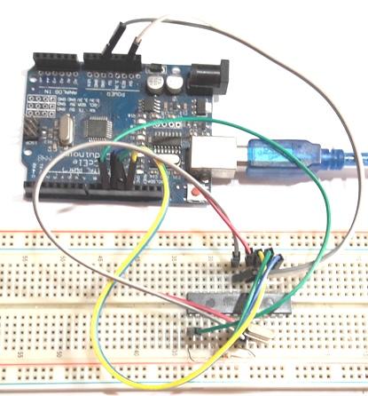
1.2 Com Arduino Nano
Colocar o arduino Nano no bred board
Atmega
pinos 7 e 8 ligados ao pino 5V do Nano
Atmega pinos 8 e 22 ligados ao pino GND do Nano
Atmega pino 19 ligado ao pino 13 do Nano
Atmega
pino 18 ligado ao pino 12 do Nano
Atmega
pino 17 ligado ao pino 11 do Nano
Atmega
pino 1 ligado ao pino RST do Nano
1.2 With Arduino Nano
Put the Arduino Nano on the bred board
Atmega pins 7 and 8 connected to the 5V pin of the Nano
Atmega pins 8 and 22 connected to the Nano's GND pin
Atmega pin 19 connected to pin 13 of the Nano
Atmega pin 18 connected to pin 12 of the Nano
Atmega pin 17 connected to pin 11 of the Nano
Atmega pin 1 connected to the Nano's RST pin
2.Software
xxxxxxxxxxxxxx
2.1 Para carregar bootloader
apenas
No PC procure o arquivo "boards.txt" que deve estar neste
caminho
......arduino\hardware\arduino\avr
Renomeie este arquivo para boards2.txt
Coloque este arquivo no lugar boards.txt
2.1 To
load bootloader only
On the PC look for the file "boards.txt" which should be in this path
......arduino\hardware\arduino\avr
Rename this file to boards2.txt
Put this file in place boards.txt
xxxxxxxxxxxxxxxxxxxxxxxx
2.2 Abra o a IDE do Arduino
Carregue o sketch ArduinoISP que
esta nos exemplos, no UNO ou no Nano.
2.2 Open the Arduino IDE
Load the ArduinoISP sketch that is in the examples, UNO or Nano.
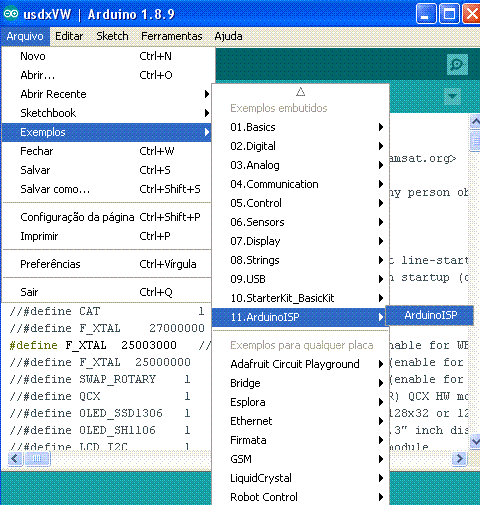
xxxxxxxxxxxxxxxxxxxxxxxxxxxxxxxxxxxxxxxxxxx
2.3 Para carregar o bootloader :
Selecione a nova placa de 20MHz.
2.3 To load the bootloader:
Select the new 20MHz card.
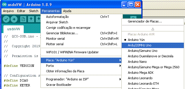
2.4 Selecione o programador
2.4 Select the programmer
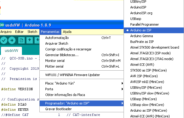
2.5 Selecione a porta USB onde esta conectado o arduino UNO ou Nano,
conectados a Bredboard.
Grave o boot loader
2.5 Select the USB port where the Arduino UNO or Nano is connected,
connected to Bredboard.
Save the boot loader
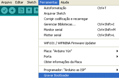
Feito
Done !
xxxxxxxxxxxxxxxxxxxxxxxxxxxxxxxxxxxxxxxxxxxxxx
3. Para gravar o sketch do USDX usando IDE1.8.10 ou superior (Windows 7
ou mais
novo)
Com sketch
arduinoisp já
previamente (visto logo cima em 2.2) colocado no chip programado UNO ou
Nano.
Abra o sketch do USDX versão W (ou o sketch que vc quiser)
pela IDE do Arduino.
Selecione no MENU
Ferramentas > Placa "Arduino/Genuino Uno" ou "Arduino Nano"
dependendo da placa programadora que vc tem...
Ferramentas > Programador "Arduino as ISP"
Muito importante :
Para gravar abra o menu e carregue usando este comando Sketch>
Carregar usando programador.
3. To record USDX sketch using IDE1.8.10 or higher (Windows 7 or newer)
With an arduinoisp sketch already previously (seen above in 2.2) placed
on the programmed UNO or Nano chip.
Open the USDX W version sketch (or whatever sketch you want) from the
Arduino IDE.
Select in MENU
Tools > "Arduino/Genuino Uno" or "Arduino Nano" board depending on
the programmer board you have...
Tools > Programmer "Arduino as ISP"
Very important :
To record open the menu and load using this command Sketch > Load
using programmer.
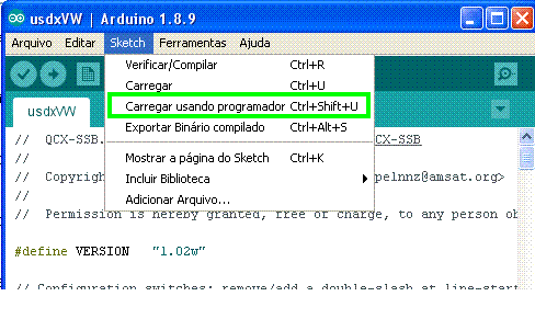
Feito!
Done !
xxxxxxxxxxxxxxxxxxxxxxxxxxxxxxxxxxxxxxxx
4. Para gerar um arquivo .HEX
Abra o arquivo na IDE do Arduino ... abra o sketch desejado.
No MENU selecione
Sketch> Exportar Binario compilado
Serão gerados dois arquivos HEX, que estarão em uma pasta
temporaria.
Um com bootloader outro sem o bootloader.
Para achar os arquivos procure pelos arquivos .hex no PC.
Não temos uma receita pronta para achar os arquivos hex.
Os arquivos HEX são legais porque para gravar no Atmega
não é necessario um bom PC e independe das bibliotecas ou
versão da IDE do Adrduino.
4. To generate a .HEX file
Open the file in the Arduino IDE... open the desired sketch.
In the MENU select
Sketch> Export Compiled Binary
Two HEX files will be generated, which will be in a temporary folder.
One with bootloader the other without the bootloader.
To find the files look for the .hex files on the PC.
We don't have a ready recipe for finding the hex files.
The HEX files are nice because to record on Atmega you don't need a
good PC and it doesn't depend on the libraries or version of the
Adrduino IDE.
xxxxxxxxxxxxxxxxxxxxxxxxxxxxxxxxxxxxxxxx
5. Gravando um arquivo .hex no Atmega
Usar o Arduino Uno ou Nano, com o programa ArduinoISP (visto em 2.2),
usar o hardware (1, 1.1 ou 1.2)
Gravar em C:\ o programa avrdude - esta
zipado
Gravar em C os arquivos de lote : grava e
tambem o testa
Edite estes arquivos para acertar a porta COM que a USB esteja
conectada e o arquivo GRAVA deve ser acertado a porta COM e o
Nome do arquivo HEX a ser gravado.
Arquivo de lote grava.bat é assim :
cls
C:\avrdude -c avrisp -b 19200 -p m328p -P COM4 -U flash:w:arquivo.hex
Como executar os arquivos testa e grava
No Windows XP Menu Iniciar>executar digite cmd e OK
No Windows 10 tecle a tecla windows + R ( a tecla Windows é uma
janelinha rerere) digite cmd
No prompt do DOS ou DOS simulado digite cd\
com tudo ligado, e estando na raiz C:\ , digite testa
se tudo OK, ele testa o CI e verifica se tudo em ordem, caso o
endereço seja 0 é que a ligação esta
errada ou com mau contato.
Se tudo OK digite grava .. ele grava e testa o que foi gravado
5. Writing a .hex file to Atmega
Use Arduino Uno or Nano, with ArduinoISP program (seen in 2.2), use
hardware (1, 1.1 or 1.2)
Write the avrdude program to C:\ - it is zipped
Write batch files in C : writes and also tests it
Edit these files to set the COM port that the USB is connected to and
the RECORD file must match the COM port and the HEX file name to be
recorded.
Batch file record.bat looks like this:
cls
C:\avrdude -c avrisp -b 19200 -p m328p -P COM4 -U flash:w:file.hex
How to run the test and write files
In Windows XP Start Menu>Run type cmd and OK
In Windows 10 press the Windows key + R (the Windows key has a little
window rerere) type cmd
At the simulated DOS or DOS prompt type cd\
with everything turned on, and being in the root C:\ , type test
if everything is OK, he tests the CI and checks if everything is in
order, if the address is 0, the connection is wrong or with bad contact.
If everything OK, type record .. it records and tests what was recorded
ZZZZZZZZZZZZZZZZZZZZZZZZZZZ
73 de py2ohh miguel