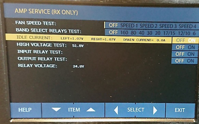
ACOM 1200s service menu, with idle current enabled
I had the request to 'take a look at' an ACOM 1200S LDMOS based HF
power amplifier, capable of 1k2 (full scale), nominal output 1k. As I
have repaired in the past without troubles my
SPE 1k3 FA PA, I initially expected that this job would be in line with
previous experience, taking maybe one hour time... but this was a
'big misjudgment' !
This PA was no longer capable of outputting more than 700W, even with 50W input, as per owner's report. - where in the past only 18 to 20W was enough to drive it 'end scale'.
In the ACOM the BLF188XR LDMOS measured on one gate 0,3V , on the other gate 0,99 V, with zero idle current (as per PA service menu, which indicated for both gates 1,07V). Remark that both gates will always indicate same value in this menu, as there is only one line to the µPC monitoring circuit ... This voltage on the menu is not reliable, you must measure with FLUKE directly between each gate and chassis ground while 'IDLE CURRENT' is turned 'ON' in service menu. If you measure different voltages on both gates, 99% sure at least one of them is defective and LDMOS must be replaced.
ACOM 1200s service menu, with idle current enabled
One gate measured to earth (PA not powered) R=82 Ohm, the other one (where 0,3V was present) R = 20 Ohm.. So, according to my experience & past repairs, I suspected one of the gates was defective and 'short circuited' to ground, normal gate voltage on BLF188XR should be around 1.9 V to produce 0,9 A idle current (Idq). No other defects (like burned components) to see. Typical cause for failure of this type (gate 'burnt' ) could be overdrive of input ...
PA module top view
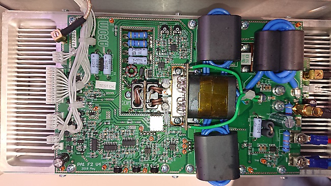
The PA module within ACOM1200S exists in different versions, the version I had to cope with was the most complex : it consists of 2 decks of PCB's, mounted one above the other. The top deck being the control, biasing & protection circuits, plus RF output transformers (one large PCB, version PA1 F2 V 4 may 2018), affixed by a multitude of screws and two connectors to the deck underneath (a couple of smaller PCB's screwed to the copper heatspreader) responsible for LDMOS input circuits, additional protections circuits etc. (2 board connected to LDMOS version PA1 F1.1 V 4 may 2018 and PA1 F1.2 V 4 may 2018).
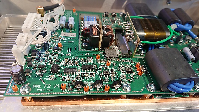
PA module top PCB

PA module bottom PCB's, with LDMOS in the middle
Last but not least, the BLF188XR was soldered to the copper heat spreader ..... excellent for heat dissipation and electric bonding, but not easy for swapping with new device ... ARGGGH... too bad :o(
I contacted the service department of ACOM who was very helpful and reactive, hereby I proposed to replace the BLF188XR (capable nominally of 1k2 CW @ 50V) by a much more rugged MRFX1k80, capable of 1k9 @ 65V, this suggestion was accepted by ACOM as being feasible (see remark further). As far as I have experienced, on HF bands (including 6m) these LDMOS are quite equivalent, except on their gate voltage required to operate in class B. The BLF required 1.9V, where the MRFX series are more around 2.6 to 2.9 V. For MRFX1K8 and 0,9A Idq, I measured for one LDMOS 2.98V, for another one 3.12V. On some other versions of the 1200S, or with factory repairs, it was seen that ACOM in fact uses the MRFX1K80 (type HR5), they solder it as well to the copper heat spreader.
Instead of sending the complete PA, or at least the PA module, to ACOM for repairs it was decided to perform the job myself ... despite knowing this would not be an easy task like with the SPE ! I had built so far several LDMOS PA's where I soldered the device to the base plate, but never unsoldered and resoldered one ...
First, the complete PA module/pallet had to be removed from PA, then stripped of completely of all PCB's till the defective LDMOs was the only part remaining on board.
For heating the copper heat spreader, I used a thermostatically regulated electric stove. To measure and set the correct temperature, I used an infrared 'pistol' digital thermometer, but attention : this will NOT work with the highly reflective copper surface.... You need to measure the temperature of the stove round surface (black), then put the copper heat spreader on it when appropriate, and wait ...
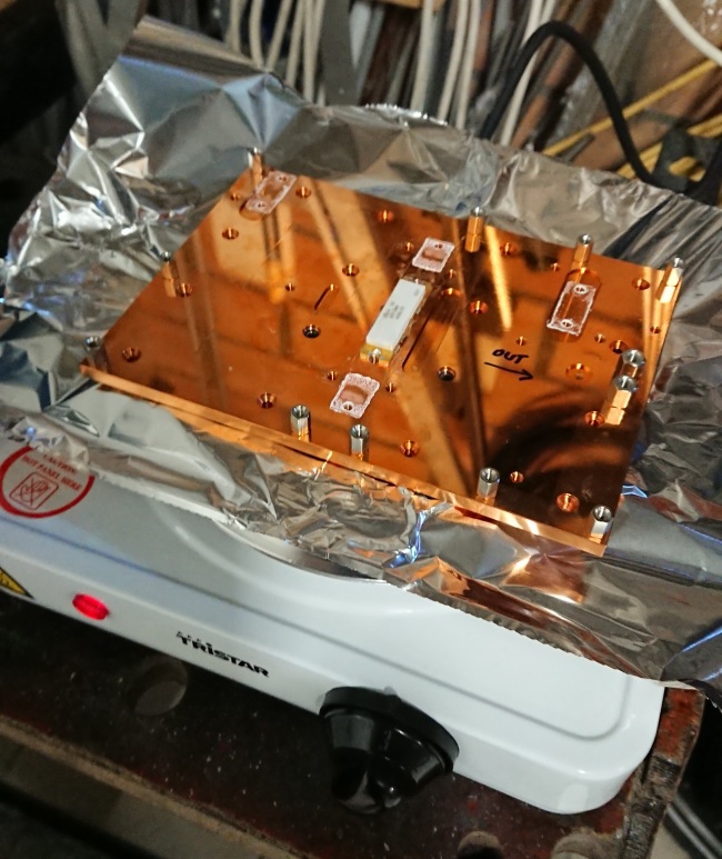
Heating the copper heatspreader to remove defective LDMOS
Once the defective LDMOS has been removed, it is imperative to clean very well the area where the new LDMOS will be seated, hereby removing any trace of the old solder - as we are not sure about it's melting point - so the surface must me absolutely flat. Wipe off the old solder when liquid, let it cool down, then carefully sand the LDMOS contact surface with very fine waterproof sanding paper (minimum P1000 type). For the removal and cleaning operation, a higher temperature than I expected was required, it must have been around 300 °C or so ... the result was that the copper surface became dull by oxidation - but this is only of 'cosmetic' importance.
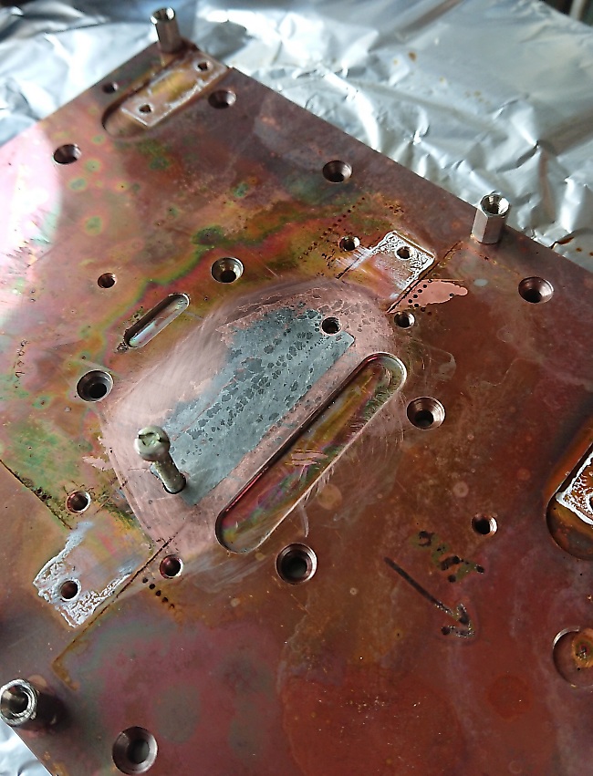
Cleaning the copper plate
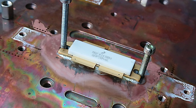
Now, before installing the new LDMOS, first measure resistance between both gates & drains to the source : all should be 'infinite'. After the solder operation, measure them again : they all still should be 'infinite' ... else for sure the LDMOS was fried :o(
IMPORTANT : then check if the two PCB's will fit with the new LDMOS ! If the gates / drain terminals are too long, it is now time to shorten them by cutting maybe 1 mm off with scissors ... because once the LDMOS will be soldered in place, the only alternative will be a DREMEL tool ... like I had to find out :o( Also check the exact position of LDMOS to align it's 4 tabs with PCB tracks, it can be somewhat off-centered ... and you only have one chance to solder it in right position !
Apply some solder flux to copper plate and LDMOS contact surfaces, and gently wipe off any excess, but try to keep the surface 'wet'. Apply special low temperature solder paste (for example MECHANIC XGS40 Special Liquid SolderPaste 158°C) on the entire LDMOS contact surface, approx. 0,3 mm thick , evenly spread (I used the blade of a cutter knife for this).
Have the electric stove heated up to 180 ... 200* C, and when temperature is OK, lay the copper spreader on it. I used two long M3 screws as 'guides' to keep the LDMOS positioned, else it will drift off it's position while 'floating' on the liquid solder ... and you risk that solder goes into the 2 screw holes. After 10 minutes or so, you can put the LDMOS in place, hereby using tweezers - the solder paste will almost immediately melt and become liquid, with the LDMOS 'floating' on it... at this stage, promptly cut the stove power, move the LDMOS back and forth laterally a couple of times, between the positioning screws, to remove any air bubbles possibly trapped under it and have the solder present evenly under the entire surface of LDMOS.
New LDMOS soldered in place, between the positioning screws
Here is an example of a MRFX1k80HR5 pulled from a PA previously repaired, where the solder was found not present over the complete surface, causing 'hot spots' and probably the reason for repetitive failures of the device ... (photo courtesy of Fabiano CT7ABD)
Now promptly remove the copper plate and put it on some cooling surface (like a flat stone). Immediately, check position the LDMOS between the 2 screws, and press it's body firmly against the copper plate (pushing on the ceramic casing with some tweezers), till the solder becomes solid again ( 1 or 2 minutes more of patience ...). This whole procedure will avoid as much as possible heat stress exposure to the LDMOS.
Let everything cool down, and measure the gates & drains resistances to the copper plate ... if all OK, the LDMOS should have survived the operation ;o)
Mount again the copper heat spreader on the aluminum heat sink, but as it's surface is not very plane, I advise to apply some heat conducting paste on the 'hot spot' under the LDMOS area - spread it well and evenly over a surface of about 5 x 5 cm. An old credit card is the ideal tool for this ;o)
Then reassemble the PCB's on the pallet, taking care that the two interconnection terminal contacts are well positioned for mating. After re-assembly, measure the resistance of gates to GND, they should both read same value of 450 ... 500 Ohm about.
For the MRFX, as already mentioned, it is required to raise the gate voltage to induce some idle current. Some components need to be replaced for this on the protection PCB (as per ACOM instructions).
ATTENTION : the trimmer (RP1) to adjust the gate voltage/idle current increases current by rotating COUNTER CLOCKWISE. So, at the start of procedure, set if FULLY CLOCKWISE - the gate voltage should be about 1 V at this moment. Some more recent versions of this amp are factory fitted with a MRFX1k8HR5, the trimmer RP1 to set the gate bias is now a 10 turn blue type - here minimal voltage which can be set is about 2,50V.
It is now time to apply 50V to the pallet and check that LDMOS is holding stand ... As a precaution, first temporarily insert a 'safety' resistor of about 5 ...10 Ohm / 5W or 10W in the + 50V line to pallet.... In worst case, at power up, you will have some smoke, but no 'big bang', and LDMOS cannot be destroyed should the gate voltage be excessive for some reason and LDMOS drawing too much current.
Using the amp service menu and enabling the gate voltage, check the pallet voltage (about 50V) and idle current which should be zero, but when adjusting very slowly the trimmer ... at some point, it will increase... good ! ... Then, passing 0,2A or so, the amp will go into error, as the 50V supply will drop because of the 'safety' resistor in line.
At that point, reduce a little bit the trimmer setting, remove the 'safety' resistor, and re- adjust again till reaching 0,9 A (with PA being cold). For one MRFX1K8 I measured 2,98V on the gates, for aMRFX1K8 of another batch I measured 3,12V was required. The voltage indicated in the service menu are irrelevant ...
Then it is time for first RF checks ... starting with low input power, perhaps 1 or 5 W on lower HF bands (80-40-20m ),... Full power (1.000W) should be obtained with 15 ... 20W max input power about, on all these mentioned bands. ATTENTION : read further for input power on higher bands !

PA back alive & kicking !
If all OK, let the PA run and warm up till 80°C (I obstructed the air intake of ventilator to speed up process...), then adjust the compensation circuit for Idle current (PA 'hot status') of 0,8 or 0,9 A.
Finally, adjust all protections as per ACOM's instructions ...
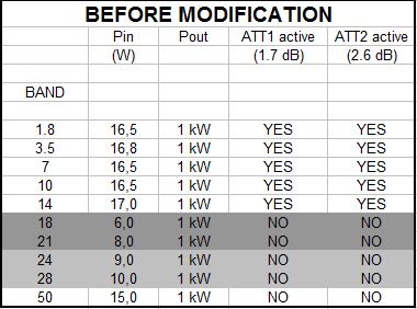
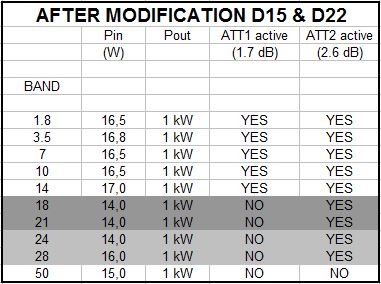
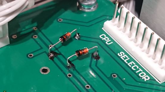
Last but not least, as MRFX1k8 has more somewhat different frequency response than BLF188XR, it is highly recommended to adapt the overall gain accordingly. This is made possible by playing with the activation of 2 T-attenuators on the PA board : ATT1 (1.7 dB) and ATT2 (2.6dB). The activation of the 2 attenuators is controlled by a diode matrix in the filter module : according to filter selected, ATT1 and/or ATT2 on PA board are active or bypassed by a SMD relay. To be noted that for 18/21 and 24/28 MHz, same band data is used.
Hereunder findings before and after modifying the control of ATT. Pin & Pout
as per ACOM's display indications, not verified by external power meter:
|
|
|
As the diode matrix is on the back of the filter PCB, it would be quite a job to dismantle the complete assembly, and I was in a lazy mood that day, so I opted for a 'quick fix ' adding D15 and D22 (1N4148 or similar) in the following manner:
In total, expect this job to last a day, taking into account the time for cooling down the pallet, testing the amp @ 80°C etc...
As a matter of facts, this repair can only be carried out by an experienced technician, with all the special material on hand, and with the support of the ACOM service department - which was very efficient and interactive in communication.
This well designed ACOM PA is fitted with many active protection features and internal devices avoiding damage by excessive voltage, current etc. But some transceivers produce a short burst of high power at key down, before going into QRP in order to drive this PA ... the time of their ALC to react.... a not so healthy situation for your PA !
LDMOS devices can withstand some mistreatments, but not indefinitely ...they are less forgiving than tube PA's ! Unlike the SPE PA, this ACOM unfortunately doesn't provide a RF power feedback to the transceiver by the ALC , in order to avoid any overdriving or reducing power when excessive SWR is present. Despite all precautions, soon or late, you will apply by mistake full transceiver output power to PA ... There is a 10 dB ATT at PA's input, but as the gates will probably fail when power exceeding 5 .. 7 W applied to them (values not specified by manufacturers), you can only hope that the PA protection will react fast enough in orde to avoid a fatal issue.
Regarding power dissipation, another major possible cause of LDMOS failures, it must be taken into account that LDMOS are mostly efficient (or otherwise said : dissipate less heat ) when being driven into saturation.
When driven into saturation, because of non linearity, the IMD products will increase in case of complex modulations, but this is not the case with 'single tone' modulations, like digital signals. So, for example, the BLF188XR will be operating much more in comfort outputting 750W CW or RTTY while being saturated under 35V supply than with 50V supply, running 18% more efficiently - this means approx. 330W less heat for the device to dissipate.
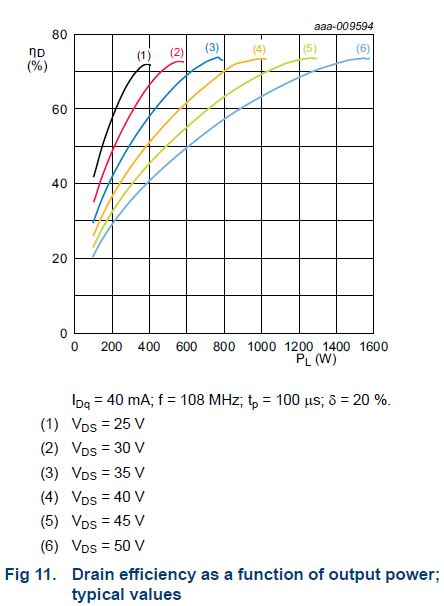
Source : AMPLEON BLF188XR product data sheet
In my opinion it is a pity that the ACOM doesn't offer, unlike the SPE, different output power settings (LOW / MID / HIGH) by adjusting the supply voltage, and allowing therefore a better efficiency and more headroom for a safe operation.
Regarding cooling of the ACOM amp, the big fan is doing a fine job, running very silently in comparison to SPE much smaller blowers.... however there is no airflow over the PCB's in order to cool the components and 'hot spots'.
Finally, I leave the appreciation of other differences between the ACOM 1200S and similar solid state PA's available on the market to every one, but from my side - comparing to SPE 1k3 FA (AT), from technical point of view:
SPE has smaller dimensions, and possibility to have a built-in ATU, as an option. Well, for me ATU is not an 'option' with solid state outputs, as they cannot run properly with SWR > 1,5 - so ATU is really a 'must' !
When fitted with ATU, SPE can store ATU's internal L/C settings in 2 memory banks. Very handy when you operate /P in the field and you don't want to loose all settings of your fixed station.
SPE has 2 transceiver inputs, with separate CAT controls, ALC, PTT, ... (ACOM only one)
SPE has 4 antenna outputs and some SO2R facility. For every band, 2 antenna's can be selected from front panel out of 4 (ACOM only one output)
SPE can operate on 4m band (with reduced power) and 60m band.
ACOM can operate remotely over Ethernet through optional 'remote eBox' and web based user interface. SPE can be remote controlled over USB or serial port (hard wired or over ip) and mimic of control panel, or as well with a web interface (by RemoteRig, or FNHW solution of HB9RYZ with RaspPi)
And last but not least ... good luck with the repairs / mods should you be ready to take the challenge !
There are 3 main causes for LDMOS failures in HAM's PA :
Excessive temperature : this cause is most easily controlled, as it is an event which is progressively taking place. Every PA has an overtemp protection. When replacing LDMOS, ensure a good thermal bonding of device to heat spreader (ideal = properly soldered = with no air or flux pockets) and avoid heat spreader temperatures of above 65°C, this will greatly enhance device's lifetime. Operate the amplifier with best efficiency possible (output power VS supply voltage).
Excessive drive power : LDMOS devices cannot withstand excessive drive power. Provide power clipping devices at the input of LDMOS to protect against short 'power spikes', for SPE amps use the ALC line to throttle back the drive power, permanently set (reduce) the power of transceiver to such level that PA cannot be overdriven. And yes, probably the PA has a protection against 'overdriving', but this is not intended to protect against 200W input instead of 20W ...
Excessive voltage at drain : The drain terminals (=outputs of LDMOS device) have some limit on permissible voltage applied, if going beyond, their junction will be damaged. In this case the gate junction will often exhibit a very low resistance (<200 Ohm) to source, instead of very high (mega Ohms). The peak voltage on drain is the sum of circuit supply voltage + RF signal (output) + extra signal due to non optimal SWR + 'possible spikes'. 'Possible spikes' can be voltages generated by abrupt switching of inductive loads, like hot switching of antenna, ATU matching networks, lightning arrestors going into conduction, a bad & intermittent contact into RF connector or antenna, ... As a precaution, for SPE amps ALWAYS use CAT control to have the ATU set the matching network according to the operating frequency. NEVER use the 'frequency sensing' or 'band select' data, this will lead into hot switching ... with possible consequences.
You will find a good analysis of possible LDMOS failure causes in this white paper (pdf document 12.3 MB).
Where as some months ago the price of MRFX1k8 was around 200,-EUR (VAT excl), same reputed and reliable suppliers are now offering it at over 1.000,-EUR / pce !
Apparently, NXP has closed down factories where it was produced and there is
a shortage on the market. Some earlier rumors have been meanwhile confirmed:
NXP will indeed step out of the power transistor market shortly. Prime
reason is the collapse in the market needs in prime areas such as
broadcasting and mobile comms. Only a very few (main stream) devices will
remain in production and will be produced with renewed production technology
(larger wafers) to gain efficiency. Investments in R&D / new types is
frozen, apart from a hand full that
is currently in finalization.