After years of faithful service, I noticed my SPE 1.3k EXPERT PA (EU
version, series 1) produced
from time to time some smell of a 'burning resistor', later some 'crackling'
noise, typical of RF flashover situations. Also, in the low and mid power
settings, it refused from time to time to amplify (despite going into TX
mode), unless I switched to high power mode, and reverted to mid or low
power ... very strange !
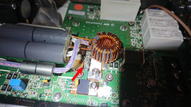
Anyway, when I opened the PA top cover and the inner cover plate, I immediately ascertained what was going wrong: the LDMOS device was dying ... despite the fact that I did not mistreat the unit (always driving it in RTTY only till 750W about in mid power setting, never reaching the 75°C temperature limit ...).
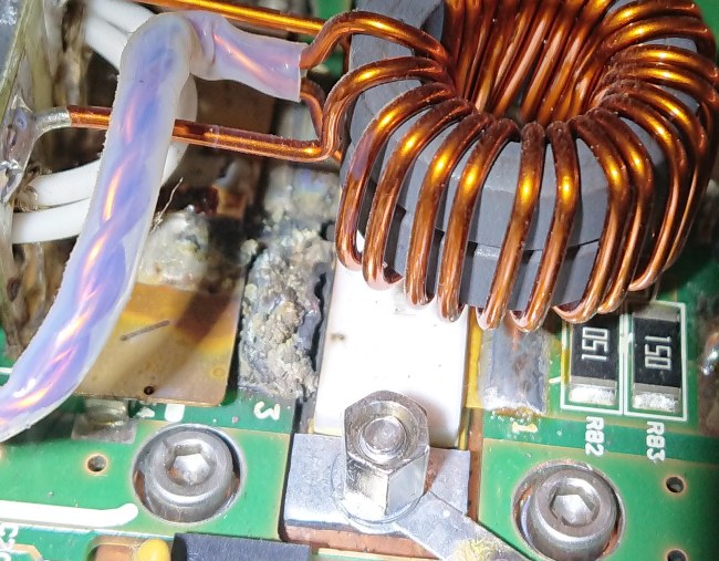
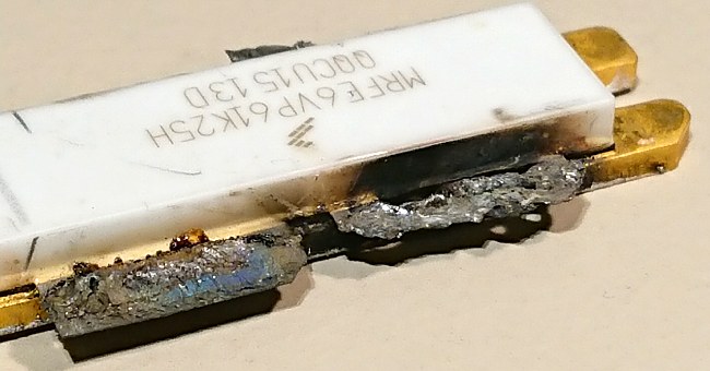
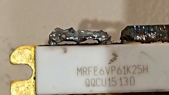
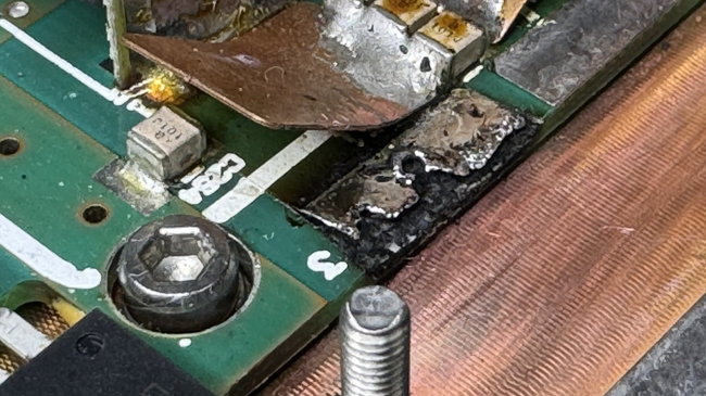
It seems that one of the LDMOS drain leads was literally 'burning up' :o( See pictures below of the MRFE6VP61K25H device pulled from the amplifier... you can see through the drain terminal !
Very strange manner in going defective ....
In my opinion, fault was due to improper soldering of the LDMOS tabs on the PCB (sorry to say so Gianfranco I0ZY). I once had to repair another 1k3FA of a friend who reported 'intermittent power output' and 'no drain current'. In this unit I found that there was solder applied on the gate tabs upper surface, but they were not soldered & electrically bonded to the PCB ... in fact just merely making contact by pressure. If same problem would be existing on the drain leads of my unit, this could lead to arcing and probably the burn-up pattern of pictures below ?
Other users have reported same problem on their 1K3. Max NG7M serviced a friend's PA and ascertained similar troubles and hereby sent me following pictures ... same LDMOS drain tab (numbered '3') as on my unit was badly damaged by arcing, the second tab was still intact, but not soldered to the PCB. However, there was some solder on the underside of drain tab (pre-tinning). VK4MA Paul had exactly same defects as myself, describing that ' one solder RF Output strip on the LDMOS had simply vapourised and the other was about to let go...it unsoldered very easily '
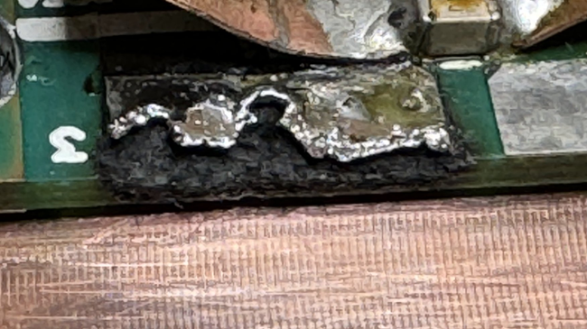
And further the German DX-pedition to TUVALU T2C had same problems : "Two of our power-amplifiers blew up in the second week, one after the other. We were able to repair one of them by re-soldering the transistors" (quote and picture below ref. EUDXF newsletter 2 • 2024) Exactly the same spot where mine blew up !

By chance, I had a MRFX1K80H (1k8 version, see specs sheet here) on hand, intended as spare for my homebrew 2m PA - so I decided to give it a try with this version. Quite an easy job, performed in less than 1 hour, as the whole PCB can remain in place ! To exchange the LDMOS, temporarily lift the toroid choke coil by desoldering it from the output transformer, as well the two solder lugs between retaining standoffs and PCB.
The best way to remove the defective LDMOS is to simply cut off it's 4 tabs with a sharp STANLEY cutter knife, inserted between it's ceramic casing and PCB edge. Once the device removed, the 4 tabs can be unsoldered one by one from the PCB with the aid of tweezers and the pads prepared for the new device.. Attempting to pullout the device on it's whole by unsoldering it's 4 tabs can lead to damage of the PCB solder tabs, as the copper heat spreader under the PCB makes it difficult to have solder melting over a big surface...
Apply really a minimum of heat paste on the new LDMOS, well smeared out evenly along it's complete surface. Be sure the copper heat spreader is clean (use alcohol and a cotton bud) and without any dust / solder particles or fibers of the cotton bud before putting the new LDMOS in place - you can check this with a torchlight illuminating laterally the trench for LDMOS.
It is VERY important that both drain tabs are making as well as possible contact with PCB foil, so not only on their outer edges. Therefore, carefully and evenly pre-tin their surface on the underside - this will ensure that they will be optimally soldered to the PCB (which is off course already tinned). Once the LDMOS is in place, start to wiggle it sidewards by applying a firm finger pressure on the ceramic body in order spread the heat conducting paste and remove some excess. In the beginning, the LDMOS will easily move, but after some time it will be like 'sticking' to the copper heat spread = perfect ! Then put back the 2 retaining standoffs, do not over tighten, but equalize gradually the pressure of both. Wait 30 minutes, and check / re-tighten slightly. Only thereafter solder the 4 LDMOS tabs to the PCB. I use for this a wedge type solder head 5mm wide of my Weller station running @ 450°C - it just takes 2 or 3 seconds on each tab to have a perfect joint!
Take care of adjusting the trimpot on the PCB (close to LDMOS) completely CCW before applying any power. This trimmer is the adjustment of idle current through LDMOS (IDq). Then, while in TX mode and LOW power setting, with NO DRIVE at all, watch the current consumption (on the display of PA, it should be 0,1 Amp) and by VERY SLOWLY turning the trimpot clockwise, set it to 1.6 A. Watch out, because beyond this value, it increases quickly (with as final result sure a 'BIG BANG'). Check the idle current on HIGH power in the same manner, it should be about 1.9 A.
Now you can test the PA, first on LOW power, then MID and finally HIGH power. After some tests to ensure all is OK, check and retighten if necessary the 2 retaining standoffs.
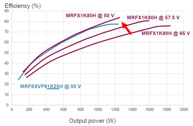
The MRFX1K80H is designed for output power of 1k8 continuous @ a supply voltage of 65V, so in the SPE amp (max 1,3 kW @ 50v ) it feels very 'comfortable'. In my howebrew PA for 2m I had to replace as well the 1k25 version (which went SK) by the 1k8 type, and found that this version was somewhat 'lazier' (less gain), because circuit components need some fine-tuning when operating at this high frequency. But on HF bands, like in the SPE, there is no difference, 1k8 version is considered as a 'plug&play' replacement, and I experienced that you will more easily reach 1k3 or 1k4 peak (SEE UPDATE BELOW !) In fact, now I usually work in 'mid power' setting, and it delivers 1 to 1,2 kW with very limited heat dissipation, where with former 1k25 LDMOS I had to run in high power mode. To minimize stress on the LDMOS, always try to run on LOW or MID power and apply enough drive to operate PA in saturation (=ALC limiting output), this will ensure best efficiency (= minimal heat dissipation) .
The following graph - provided by NXP - clearly shows that the MRFX1K80H is more efficient running on 50v @ 1k2 output power on 27 MHz than the MRFE6VP61k25 version, without retuning of any components:
It seems that SPE is now factory fitting in the 1k3 PA (series 3, possibly 2 as well ...) the 1K50 LDMOS plastic case version instead of 1K25 and soldering it to the copper heat spreader.... and if it fails, replacing it with some extra protections / modifications to avoid overdriving by adding 4 zener diodes (3V9 and 8V2), a (wire wound ?) 56R resistor in it's gates, and an AQV214E PhotoMOS device as additional attenuator on the input transformer, which turns on in case of excessive SWR or by the µprocessor - see pictures below. (PA of F4AZF Damien - see further for repairs ....).

Resistor 56R and zeners as protection
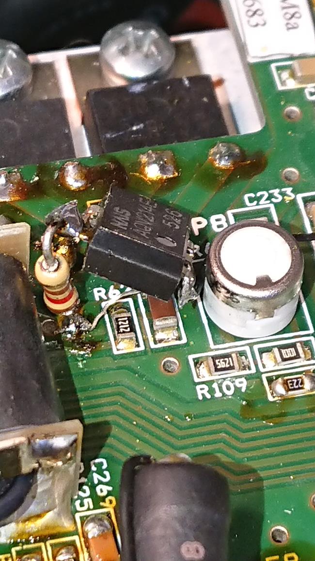
PhotoMOS device AQV214E and resistor 120R on input Xformer
After one year of intense but trouble free operation with the 1k8 device, during the CQWW contest of October 2021, while operating full power in SSB on 160m, the PA suddenly delivered no more output power.... While going in TX mode, no more idle current drawn, and rig output power was limited to 20W due to the ALC feedback of SPE. Most probably, while in TX or going into TX mode, there was an unintended band change and hot switching due to erratic CAT signals resulting from collisions of polling information from N1MM and another logging software.,... The SPE regularly had run before several times into protection ('Band not allowed') due to this error. So, YES, I admit this was entirely due to my mistake :o(
But why was the rig delivering 20 W, being throttled by the ALC feedback ?
On the input circuit of the PA (EU version), there is a T resistive network (2x 22R with 47R), providing 8 dB of attenuation. According to manufacturer's specs, the LDMOS requires 3W (+ 35 dBm) input to provide full output (going into compression) of 1,2 kW @ 50V. Adding 8 dB of the input attenuator, the result is 43 dBm or exactly 20W !
For information, hereby the drive level required (as per SPE information) on the 1.3K FA EU model (not knowing which series ...), specified per band and power setting:
I immediately checked the LDMOS - which was visually in an immaculate condition - and ascertained that in TX mode the gate voltage was only 0,3 V instead of about 2,5 - 2,7V ! So obviously there was a problem with the gates ... most probably they were dead due to overdriving (In general, LDMOS go SK due to 2 reasons : either overheating, or too much input power).
Replaced the LDMOS with another 1k8 device on hand and measured how much power was required to drive it up to 1.3 kW - depending on bands, in RTTY mode about 5W or so... much less than the 20W limit defined by the ALC ! So I decided to attenuate the drive level applied to LDMOS to keep it on the safe side. On the PCB , close to the input transformer feeding the LDMOS and next to the idle current adjustment trimpot, there is a wire jumper which can be removed and replaced by a resistor - I found that a 36 Ohm / 5W out of my junk box did the job ! However, this had the effect of limiting the maximum output power on the 6m band. To compensate for this, I placed a 270 pF dipped mica capacitor over the 36R resistor (which on 6m has a reactance of about 12 Ohm) .
Next step to avoid overdriving was to place some Transient Voltage Suppressor (TVS) diode(s) on the LDMOS gate input circuit. Hereby take into account that a TVS exhibits a high capacitance (in general > 300 pF) and therefore attenuates the RF signal, even when not conducting. So always consider 2 TVS diodes with each in series a signal diodes (e.g. 1N4148 with 4 pF). For limiting the input power to 3W, it is expected that the RF voltage will reach about 12,5 V RMS maximum, or 17 V P-to-P. A TVS of 15V should be fine, like the BZW06-15B.
I observed the voltage/signal with a scope on the TVS to ascertain it has some effect - it will mitigate the excessive drive power (the RF sine wave will have some flattopping) - but do not consider this as an absolute solution.
See picture below taken while 'works in progress". The two TVS/1N4148 were added on the left side of resistor, towards a ground point on PCB left of the SO2R socket. The 270pF capacitor is next to 36R resistor.... (note : I have seen similar added protection put in place by SPE on EXPERT 1k5 after repair at their factory ...)

According to some sources, it is recommended to set the transceiver output power to maximum, and let the ALC do it's work .... In my opinion, it is more prudent to set the maximum output power of TRX to such level where the PA can deliver it's full power on HF and 6m band, but not beyond. Under these conditions, the LDMOS cannot be stressed by excessive power on it's input ... even should the ALC plug on the TRX or PA be removed by inadvertence. Driving it with my IC-7610, output power is ALWAYS limited to 15% for HF and 6m bands. (or about 15W).
Some people only use their PA occasionally, being afraid of blowing it up, and soon or later will forget to reduce the TRX maximum power when occasionally using it ... a 'small mistake' with the inevitable same outcome. Yes, on all LDMOS PA's there is some form of protection against overdriving, but not against driving it with 100 or 200W ! Don't blame the manufacturers for this ... Unlike using the PA occasionally, I am convinced it is more prudent to ALWAYS use it and (1) use the ALC line (2) properly adjust maximum output power or TRX.
Attention ! A user has reported me having fried his MRFX1k8 in his EXPERT 1.5 already 3 times, despite utmost care ... never running on MAX power, perfect SWR, never setting his rig to more than 25W out, using the ALC interconnection.... Again, for a fourth (!) time, no power out and bias voltage on gates found as zero, indicating shorted to ground. Why these repetitive defects??? It turns out his rig is the Kenwood TS-990 'flagship' model, which needs -7,5 to -10V on the ALC input to reduce power instead of the 0 to -4V standard level generally found on transceivers. In my humble opinion, it is probable that the EXPERT will only deliver this -7,5 to -10V while being seriously overdriven, with result of one or two gates of LDMOS being eventually damaged ... I would therefore advise to insert a voltage converter (op-amp circuit with 2 or 3x gain) in the ALC line to have the transceiver ALC react properly.
Anyhow, since my EXPERT has been fitted / modified with the MRFX1k80 it has been running fine, for use at home (in RTTY, FT8, ...) or operating 24h full power and non-stop during contests in the field ....
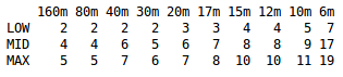
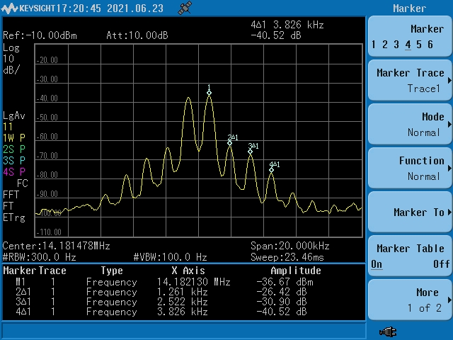
Important remark : According to ITU Rec. ITU-R SM.326-7 (download) for single-sideband single-channel radiotelephone emissions (R3E, J3E, H3E) without a privacy device the acceptable intermodulation level can be taken as –25 dB or less. The intermodulation level considered here is expressed in terms of the ratio, generally in decibels, between the powers of the largest intermodulation component at radio frequency p(F0 +/- f1) – q(F0 +/- f2) - with p, q = 1, 2, 3, etc - and the power of the fundamental component at radio frequency (F0 +/- f1 or F0 +/- f2) produced by either of the two f1 and f2 modulating oscillations applied simultaneously at the input of the transmitter. Because of this, the average or mean power (as you will read from a wattmeter if only one tone present) will be 2x higher (+3dB) and the PEP power (= when the 2 peaks of modulation are in phase) will be 4x higher (+6 dB) than the power of each single tone f1 or f2, therefore 6dB must be ADDED to the difference between one fundamental tone f1/f2 and first IMD product . E.g. in the screenshot below, IMD is better (according to ITU) than 26.42 + 6 = 32,42 dB . (If in doubt about 'power per tone', 'average/mean power' and 'Peak Envelope Power (PEP) see pdf document and pdf document)
Two tone test with bare IC-7600, ALC just coming up, Po 15W mean power

Two tone test with SPE 1.3k PA, LOW power setting, 500W mean power out

Two tone test with SPE 1.3k PA, LOW power setting, 800W mean power out
Two tone test with SPE 1.3k PA, HIGH power setting, 1000W mean power out
This is the third MRFE6VP61K25H device that I am sending into semiconductor's heaven ... I have the impression that, since these very first high power devices went into production, a lot of research and improvement have been made by manufacturers to make them more reliable, resulting in the 1k5 and 1k8 versions.
The repaired PA was stress-tested in 2022 IOTA contest for our running station in CW, operating continuously during 24hrs @ 'medium power' setting, providing effortless 1kW out, under ambient temperatures of up to 25 °C, the displayed temperature never exceeded 39°C (fans programmed for 'contest mode') . Again running well during IOTA contest 2024 edition, 24/24h SSB @ 'medium power' output.
This PA was defective after a couple of hours operation and sent back to SPE for repairs. It came back with some modifications - see pictures above. LDMOS is MRF1K50N type, soldered to copper pallet. After a second failure, I was asked to have a check on it ... took it as a challenge for a friend ! LDMOS was found with one gate shorted to ground (SOURCE). Replaced 1K50 type by the much more rugged 1K8 version, but bolted to copper heat spreader, in order to make possible subsequent repairs more easy ! Copper heat spreader surface was first carefully polished and LDMOS affixed according to the rules. If all precautions are taken regarding a decent heat transfer, bolting down a LDMOS has no disadvantage vs. soldering on the pallet - I never broke down a device due to thermal runaway or excessive heat. But yes, sure soldering is better ... the choice also depends on the subsequent 'serviceability' of the equipment. Replacing a bolted LDMOS in these amps takes less than one hour, but for a soldered one will take 4 to 6 hours and is a much more risky and complex operation ...
Attention : for the 1K8 version you need a somewhat higher gate voltage (Vg) to induce quiescent current on drains (IDq) than on the 1K50 version. With R65 trimmer resistor (on the right side of AVQ214E in one of above pictures) could only set between 2,52 and 2,90V, what is just too low for 1K8 which needs 2,95 to 3,15V about for 1,0 to 1,5 A IDq. With R70 (22k, marked 223 in same picture, under the R65 trimmer) removed, I could vary the Vg between 2,80 and 3,22V = IDEAL ! So I could set IDq @ 35°C at 1,4 A under MAX power, when at room temperature of 20°C, it measured 1,1A.... perfect !
There are 3 main causes for LDMOS failures in HAM's PA : Excessive temperature : this cause is most easily
controlled, and most unlikely to happen, as it is an event which is progressively taking place. Every
PA has an overtemp protection. When replacing LDMOS, ensure a good
thermal bonding of device to heat spreader (ideal = properly soldered =
with no air or flux pockets) and avoid heat spreader temperatures of
above 65°C, this will greatly enhance device's lifetime. Operate the
amplifier with best efficiency possible (output power VS supply
voltage). AMPLEON offers a nice 'RF Power Lifetime Calculator' tool to assess MTF (Mean
Time
between Failure) of their ART LDMOS, see
https://www.ampleon.com. So for a 2kW device, running at full power
(2.000W out, ID 39A, VD 65V) and case kept at 65°C (junction temperature
will be 106°C) MTF will be almost 10.000 years. For a casing kept
at 100°C (junction at 141°C) MTF will be 1.000 years about. What is also
interesting : if the device is running at 50% of it's capacity instead
of 100%, expected lifetime is multiplied by a factor of 10 ! But
OK ... is the difference between 1.000 years and 10.000 years really
relevant ? Excessive drive power : LDMOS devices
cannot withstand excessive drive power. Provide power clipping devices
at the input of LDMOS to protect against short 'power spikes', for
SPE amps use the ALC line to throttle back the drive power,
permanently set (reduce) the power of transceiver to such level
that PA cannot be overdriven. And yes, probably the PA has a protection
against 'overdriving', but this is not intended to protect against 200W
input instead of 5 or 10W ... Excessive voltage at drain : The drain
terminals (=outputs of LDMOS device) have some limit on permissible
voltage applied, if going beyond, their junction will be damaged. In
this case the gate junction will often exhibit a very low resistance
(<200 Ohm) to source, instead of very high (mega Ohms). The peak
voltage on drain is the sum of circuit supply voltage + RF signal
(output) + extra signal due to non optimal SWR + 'possible spikes'.
And yes, LDMOS devices can possibly withstand 'infinite SWR'... But
'possible spikes' can be voltages generated by abrupt switching of
inductive loads, like hot switching of antenna, ATU matching
networks, lightning arrestors going into conduction, a bad &
intermittent contact into RF connector or antenna, ...
As a precaution, for SPE amps ALWAYS use CAT control to have the
ATU set the matching network according to the operating frequency. NEVER
use the 'frequency sensing' or 'band select' data, this will lead into
hot switching ... with possible consequences. For example maximum
DRAIN-SOURCE voltage specified for MRF1k2 = 125V, MRF1k5 and BLF188 =
135V, MRF1k8 = 179V (43% more than 1k2 version). You will find a good analysis of possible LDMOS failure
causes in this white
paper (pdf document 12.3 MB). Where as some months ago the price of MRFX1k8 was around 200,-EUR (VAT
excl), same reputed and reliable suppliers are now offering it at over
1.000,-EUR / pce !
Apparently, NXP has closed down factories where it was produced and there is
a shortage on the market. Some earlier rumors have been meanwhile confirmed:
NXP will indeed step out of the power transistor market shortly. Prime
reason is the collapse in the market needs in prime areas such as
broadcasting and mobile comms. Only a very few (main stream) devices will
remain in production and will be produced with renewed production technology
(larger wafers) to gain efficiency. Investments in R&D / new types is
frozen, apart from a hand full that
is currently in finalization. 
Copper heat spreader surface was polished with fine sand paper 1200 and oil. On the
left, R76 tiny NTC to take care of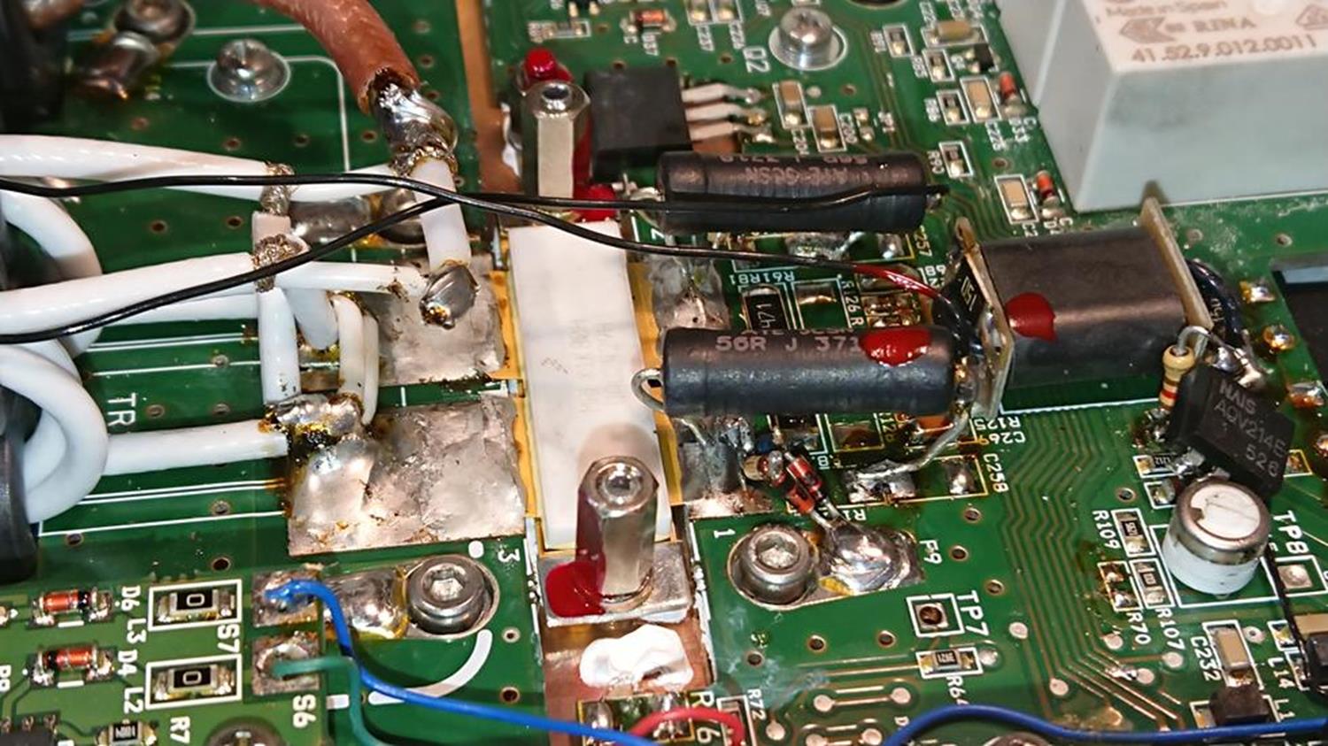
1K8 version after repairs ... a solid 1k3 PEP out (1,1k CW on the BIRD)! Click
image to ZOOM
Why do LDMOS breakdown ?
Prices of MRFX1k8 have gone up sky high ! (summer 2025)