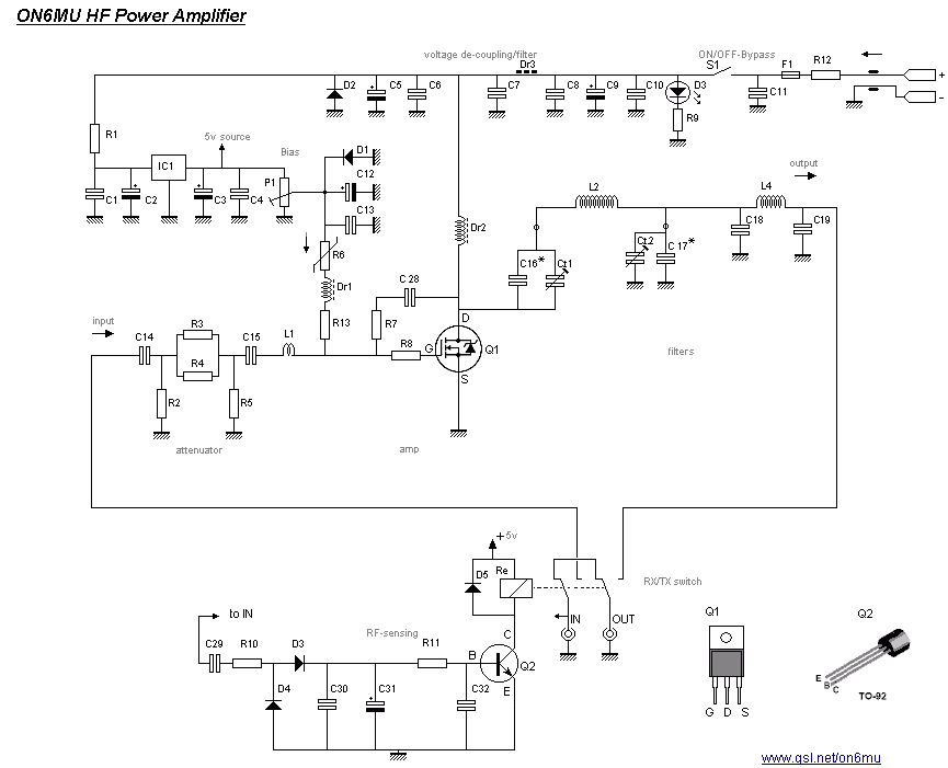
Allmode HF band RF Linear Power Amplifier
for HF: 40, 30, 20, 17 and 15* meterband
![]() 's
's
Allmode HF band RF
Linear Power Amplifier
for
HF: 40, 30, 20, 17 and 15* meterband
RE-PA30HF5C

By Guy, de ON6MU
RE-PA30HF5B rev1.1b
oct/09 5 band switchable replaced/discontinued
Rev2.2 feb/25
Prototype

Download Gerber Files for the PCB, made by Adrian
VK3LK
About the Linear HF amplifier RE-PA30HF5C (prototype)
This project uses a widely
available IRF510 MOSFET. This N-Channel enhancement mode silicon
gate power field effect transistor is an advanced power MOSFET
designed, tested, and guaranteed to withstand a specified level
of energy in the breakdown avalanche mode of operation.
MOSFETs operate very differently from bipolar transistors.
MOSFETs are voltage-controlled devices and exhibit a very high
input impedance at dc, whereas bipolar transistors are
current-controlled devices and have a relatively low input
impedance. Biasing a MOSFET for linear operation only requires
applying a fixed voltage to its gate via a resistor.
The built-in self-regulating actions prevent MOSFETs from being
affected by thermal runaway, but still needs some thermal
protection (R6). MOSFETs do not require negative feedback to
suppress low-frequency gain as is often required with bipolar RF
transistors.
I chose the IRF510 because lots of hams use 'em and they're
cheap. But they perform a bit less when it comes to constant gain
and/or power output across a wide range of frequency bands. I
wasn't especially concerned with that, and the advantages
outweigh the contra's, so I went with that MOSFET.
Rather than using a 1:4 toroid (which is excellent) to match Q1 impedance to 50 Ohms, I have applied the "old school" radio valve coupling; impedance matching circuitry between the output and the antenna using a L-filter...Why? FET devices are more closely related to vacuum tubes than are bipolar transistors (and because I do like to do things my way HI). Both vacuum tubes and the FET are controlled by the voltage level of the input rather than the input current. They have three basic terminals, the gate, the source and the drain. These are related and can be compared to the vacuum tube terminals. The ralationship between the two doesn't stop here...The two most important relationships are called the transconductance and output. An advantage of MOSFET devices is that they do not have gate leakage current and MOSFETs do not need input and reverse transconductance.
The amplifier is made to be
driven by transmitters in the ½ to 2 watt range. Built-in to the
power amplifier is a sensitive (Q2) T-R relay which will switch
the unit in and out of the
antenna line. When in receive, the amplifier is bypassed and the
antenna feeds directly to the input jack, when you go to
transmit, the T-R circuit detects the transmit RF power and
automatically switches the power amplifier into the circuit and
amplifies the applied RF power. If you decide to run
"barefoot" turning off the AMP it will disable the
amplifier and your QRP
transmitter will feed directly through the amplifier without any
amplification.
Power is supplied by any 14 to 25 volt (or 2 x 12v battery) DC
source with a current draw of 1 to 2 amps depending upon RF power
output and applied voltage.
The linear amplifier can be used with QRP SSB/CW/FM/AM/PSK transmitters on any of the amateur bands between 40m...15 meters. 80m band is still highly experimental. It works but with with limitations; Any feedback is welcome.
The completed amplifier will reward the builder with a clean, more powerful output signal for a QRP rig when radio conditions become marginal.
Band selection
Switching beween bands could be done manually using a rotary
switch.
You can build the amplifier for only one band or a combination of
any other of the five available bands.
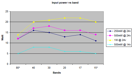
Drive
The input drive can be anything from 0.3watt to 1.5 watt (2 watt
is outer max), which will be amplified to +/- 20 watt
respectively.
The output varies on the drive power, frequency and the applied
voltage.
Power
The power output is not perfectly linear to the input
frequency/band. The impedance 50 Ohms match could be solved by
using a 1:4 toroid, or as I like to use, the "old
school" radio valve coupling; impedance matching circuitry
between the output and the antenna using a L-filter...And, the
IRF510 isn't perfect (note:
there are also low grade versions of the Mosfet out there which
can lower the output power and influence the quality of the
signal/waveform).
The N-channel mosfet has an input capacitance thats a bit on the
high side and the output capacitance that varies with the cross
over frequency. It can be a slight problem when it comes to
constant gain and/or power output across a wide range of
frequency bands. I wasn't especially concerned with that so I
went with this MOSFET anyway. Of course the main issue was the
simple design to be able to use one band or even up to five bands
if wanted, which always has some compromise in this type of
design. This means that there is some fluctuation of the output
power par band.
When driven between the optimal
range of +/- 1 watt to 1.5 watt the amplifier more than capable
to deliver 20 watts +/- 5%. Output power for AM should be set to
+/- 50% of max.
Although the design allows you to work in a varied range of
voltages, the maximum output is only guarenteed @ 24volts.
I'm sure if you peak the amp close to perfection for one specific
band you could get more power. Quality of all components,
construction etc also influences the performance.
I used breadboard to build my protoype and some "dead
bug" work. Dead bug prototyping and freeform electronics are
a way of building working electronic circuits, by soldering the
parts directly together, or through wires instead of the
traditional way of using a printed circuit board (PCB.)
Graph:
Input/Output Power vs Voltage
Higher power than 2 watts does not improve linearity and could damage the mosfet.
Bias
The power amplifier require biasing for proper RF
performance. BIAS has be applied to Q1 to have clean proper and
correct SSB modulation using this amplifier. Set P1 so that +/-
120 mA current flows through Q1.
Thermal
protection
R6 is a PTC resistor that allows which is used here for thermal
protection. As the resistor heats up the resistance increases,
which lowers the bias voltage. R6 should be placed near Q2.
Modulation modes
If proper BIAS to Q1 is applied, you can amplify any type of
modulated wave.
Output power for AM should be set to +/- 50% of max.
Filter
RF purity and harmonic suppression is done here. Also allowing
the FET to be coupled to the antenna system through antenna
impedance matching circuitry (C16, Ct1, L2, Ct2, C21, C26, L4,
C27). Care is taken at this stage so that no harmonic frequency
is generated which will cause interference in adjacent
band/harmonics on other bands. This 4-element L-type narrow
band-pass filter circuit and a 3 element low-pass Butterworth PI
filter for the desired frequency removes out any remaining
harmonic signals efficiently.
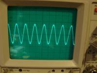
A picture from my oscilloscope:
RF-sensing
The basic principle of RF-sensing using a relay is clearly
drawn in the schematic and pretty much self explaining.
Tip: I would like to recommend to add a mini-switch between C31
and GND if you plan to use it for CW modes. The on-time is to
long for continues wave modulation formats.
Input Attenuator
I made provisions to include an RF attenuator consisting out a Pi
network of R2, R3/R4, R5 which gives a Forward Attenuation of
3.63 dB and a Input Return Loss of 23.23dB. There are numerous of
reasons why I implemented it in this design. It improves overall
linearity, achieves some "protection" and enhances
stability of the drive input (being a transmitter, transceiver)
and Q2 gate.
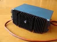
Cooling/heatsink
Q2 needs to be mounted isolated from the heat sink. Use proper
thermal grease and isolator.
I used an old P3 heat sink, which work just fine.
 I mounted a Pentium 3 heatsink on the back of the
alu-casing. A square space is cut out of the back of the alu-box
to allow Q2 to be screwed onto the heatsink. The heatsink is
firmly mounted on the back of the chassis with thermal grease
allowing the chassis as extra cooling surface.
I mounted a Pentium 3 heatsink on the back of the
alu-casing. A square space is cut out of the back of the alu-box
to allow Q2 to be screwed onto the heatsink. The heatsink is
firmly mounted on the back of the chassis with thermal grease
allowing the chassis as extra cooling surface.
Construction considerations
HAMs that are experienced in constructing RF projects will know a
number of possibilities to create a good RF design.
Note when using a band switch selector: Because I started from
scratch and still was in experimental/design stages I have placed
the capacitors/trimmers of each band directly around the switch.
This works when short connections are used. You can however
solder them directly to the PCB. Always start with the lowest
band and set the capacitors to maximum output and work are way up
from there. Also set your transceiver to the middle of the (each)
band segment..
I mounted a Pentium 3 heatsink on the back of the alu-casing. A
square space is cut out of the back of the alu-box to allow Q2 to
be screwed onto the heatsink. The heatsink is firmly mounted on
the back of the chassis with thermal grease allowing the chassis
as extra cooling surface.
One thing on the trimmer capacitors (Ct1x and Ct2x). Do not use
plastic trimmers, they will melt and perhaps burn through causing
shortening and possible failure of Q2 and who knows what else.
Please use air- or ceramic based trimmers.
If you do not have them, then the only way tweaking the amplifier
is by trial-and-error, (C16x and C17x).
Use a choke (or a snap-on ferrite bead) at the point where the
Vcc wires leave the alu-box.
Try to limit the maximum current to 3 Amp (F1). I placed a 1 Ohm
resistor R12 in series to buffer a minimum the maximal current
and peak at power up.
Use small 50 Ohm coax between the in- and output of the PCB
connections to the SO-239 connectors.
Enclosure Recommendations
To accomplish RF shielding the whole circuit needs to be
mounted in an all-metal/aluminum case.
Please take look at Adrian VK3LK designs!
Grounding
To prevent ground loops, spurious oscillations etc. please
take attention to:
- decouple the PCB in the chassis (housing)
- all connections and wire leads should be made as short as
possible
- a proper PCB layout with enough ground surface ensuring normal
ground paths
- the source of Q2 (IRF510) should also be grounded to the
chassis as close as possible
Specifications RE-PA30HF5C
Allmode: AM/FM/CW/SSB/FSK
Bands: 40m, 30m, 20m, 17m, 15m* (15m band needs further tweaking, 80m needs further investigations)
Average
output RF power: +/- 20W @ 24v
Quality of all
components, construction etc also influences the
performance. I build it on breadboard and some "dead
bug" work. It's a prototype and always under
construction HI.
Works great
with Yaesu FT-817, Ramsey QRP rigs or any other 0.5-2
watt transmitters
Input power drive: 250mW...2watt top peak max (ideal
1.5watt)
All modulation modes
Efficient band-pass type harmonic L-filter + lowpass Butterworth PI filter
Usable voltages: Vcc 13.8 - 25 volts
Average current I: +/- 1.9A @ 24v at full load, minimal 0.8A @ 14v
Built-in T/R relay automatically switches between receive and transmit
VSWR overload resistant (short period of time, not unlimited!)
Multistage
band pass and low pass filter for a reasonable clean
signal
+/- -40dBc on 2nd harmonic
Optional: Manual band switching (if build for more than one band)
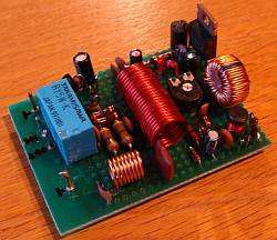
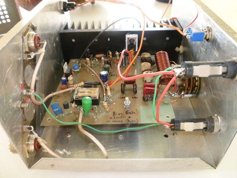
The 5-band HF power amplifier "insides" (this pic shows the version with band switch)
The MOSfet HF-band Amplifier settings
Needlessly to say,
but I will say it anyway, before testing anything please be sure
to double check every connection. The project should be finished
HI.
Connect a proper dummy load and a power meter to the output of
the amp. Also put a Ampere meter in series with the Vcc, allowing
monitoring of the current during the setup.
Set all trimmers (Ct1 & Ct2) half way (in medium setting).
Set P1 to the ground (zero ohms).
Now gently increase the voltage to the amplifier while checking
the current till you reach 18 volts. The only current you should
see is a the liddle idle current of Q1 (a few milli amps and a a
few mA of LED D3 if connected). We do not need the full 24 volts
during the tuning/setting stages.
Now gently turn P1 till you get approx. 120 mA.
So far so good? Now we need to check if the (Q2) RF-sensing
circuit is working properly (Although
I would like to recommend to test this before anything, rather
than building the entire project and test it. Or at least before
mounting the PCB in the alu-box, and without Q2 soldered. The
RF-sensing ON-time can vary according to the relay used).
Connect your transceiver (or other drive) to the input, and set
it to the lowest power rating of +/- 0.5watt and set your
transceiver to the band you designed this amp for and place it
CW/FM.
Be sure the dummy load is still at the output of the amp.
Key your transceiver and if all goes well the relay (Re) should
power up and you should see the current rise and your power meter
should already show an amplification of the RF input power.
Also set your transceiver to the middle of the (each) band
segment.
All working as planned? Excellent! Now we need to tune the
filter-unit by setting the Ct's to maximum output.
Set the drive power (your transceiver) to +/- 1.5 watts or less
At 14 volts the average amp would be around 0,8 amp,
Current should be around 1.9 Amp +/- max @ 24v (depending on the
voltage, input power and output impedance which should be 50
Ohms).
Note if working with a band switch:
Turn the band switch (if used) to the lowest frequency/band, as
we start with the lowest band and work are way up from there.
If you build the amplifier for more than one band, next is to
repeat the above for each band and setting the Ct capacitor
trimmer(s) according to each band respectively.
After the filter is tuned in respect to each band you can
increase the voltage to 24 volts. Check everything again, band by
band. Could be that you notice a slight difference in the peak
output power, do to the capacity of the switch and the filter
components. Just re-tune (if needed) each trimmer (Ct1...Ctx) for
each band respectively.
The maximum current of the amplifier should never exceed 2 amps.
RF-sensing
considerations
The basic principle of RF-sensing using a relay is clearly
drawn in the schematic and pretty much self explaining. Q2
(BC338, 2N2222) will conduct when RF energy is applied at the
input of the amp (via R10, C29, D3, D4, C30 biasing the base of
Q2) hence powering up a RF capable relay. This relay switches
between RX and TX with amp. When no Vcc is applied to our
amplifier (and so Q2 too) no amplification is done bypassing the
amplification. The input is simply re-directed directly to the
output (as if your transceiver is connected without an amp). The
RF sensing circuit is sensitive enough to react on .5 watt
easily.
To allow the amplifier in SSB-modulation some extended PTT
time-on the RF-sensing unit (Q2->relay) has to be increased.
C31 adds the needed "breathing" time. In FM/CW/AM/FSK
modes a carrier is present and extended PTT time-on of the
amplifier isn't needed, hence can be short.
Important: Everything will be within specs if you use RY5W relay,
but timing delay (the "breathing time") can vary on the
type of relay used (Ohms resistance value of the relay coil),
hence experimentation of C31 is needed.
Although this example of RF-sensing isn't the Worlds most best
sollution, it is pretty easy for beginners and effective though.
Better would be to drive Q2 from your transceiver (amp drive) as
this will switch the amp at the very moment of PTT.
Tip: I would like to recommend to add a mini-switch to disconnect
C31 if you plan to use it for CW. The delay is too long for those
modes.
Note:
Always use a dummy load for
testing and adjusting the amplifier!!!
Remember that this is a prototype.
Parts list 5-band HF power amplifier
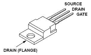
Q1:
N-Channel IRF510 MOSFET
(with proper heatsink isolated from the mosfet)
Q2: NPN BC338/337, 2N2222...
IC1 = 78H05 or 78L05
C1: 100n
C2: 1uF/50v
C3: 1uF/16v
C4: 100n
C5: 2.2uF/50v
C6: 100n
C7: 4.7nF
C8: 4.7nF
C9: 220uF/50v
C10: 100n
C11: 47n
C12: 1uF/16v
C13: 68n
C14: 100n
C15: 100n
C16: all
150...200volt ceramic
15M -> 30p
17M -> 39p
20M -> 68p
30M -> 180p
40M -> 2 x 150pF parallel (or 330)
(still under test!!! 80M* -> 2 x 220pF parallel (or
470), NOTE: 80m band is stil experimental, power goes
only to 14watt. Needs further
investigation/experimentation. Still under test!!!! Ant
feedback is appreciated.)
C17: all
150...200volt ceramic
15M -> 100p*
17M -> 120p
20M -> 220p
30M -> 240p
40M -> 470p
80M -> 1200p NOTE: 80m band is stil experimental,
power goes only to 14watt. Needs further
investigation/experimentation. Still under test!!!! Ant
feedback is appreciated.
C18: 220, ceramic 200v
C19: 100, ceramic 200v
C28: 2n2
C29: 470p
C30: 47n
C31: 68uF/tantalum 16v (determines the ON-time for RF-sensing)
C32: 150n
Ct1:
0...100pF ceramic or air-spaced trimmer
(for 15M to 20M: 0...40pF)
(for 20M to 80M: 10...100pF)
Ct2: 0...40pF ceramic or air-spaced trimmer
R1: 47 1/2w
R2: 390 1/2w
R3: 47 1/2w
R4: 47 1/2w
R5: 390 1/2w
R6: 470 PTC
R7: 1k
R8: 10 1/2w
R9: 18k
R10: 1k
R11: 1k
R12: 1 Ohm - 5 watt
R13: 560
P1: 5k potentiometer (BIAS setting Q2)
D1, D3, D4: 1N4148
D2, D5: 1N14001
S1: Toggle switch (ON/OFF-Bypass)
S2: 5-position quality switch (if possible silver plated)
2 x SO239 connectors
Re: RY5W-K relay
F1 = 2 amp slow
Alu-box
Heatsink + thermal grease
Dr1: ferrite core 3mm diameter, 5...8mm long. 40 turns, 0.3mm wire (+/- 5uH)
Dr2: FT50-45 core with approximately 20 turns (equal 150uH, thanks VK3LK) (rev 2.2)
Dr3: a ferrite bead with 4 turns of 0.6 mm wire
L1: 29nH; 2 turns, no spacing, 5 mm inside diameter, 0.6mm wire
L2: 1.4uH; 22 turns close together, 1.2mm enameled wire. Inside diameter is 9.5 mm (27mm long)
L4: 150nH +/- ; 8 turns close together of 1.2 mm enameled wire. Inside diameter is 6.5mm (10mm long)
Coils
All we need to do
now is make a few remaining coils that have to be handmade - for
that "old-world craftsmanship" touch!
The wire used for the coils are enameled wire (stripped from any
AC transformer).
For 80M band you need an additonal coil in series with L2.
Secondary coil for 80M Coil specs: 3.2uH; 15 turns close
together, 0.6 mm enameled wire. Inside diameter 9 mm and 14mm
long. You could add the numer of turns to L2 making one coil if
you would use this amp only for 80M band. All feedback is welcome
as this band needs further tweaking and is experimental still
with this amp!!
Dr1: you need a ferrite core of 3mm diameter and about 5...8mm long. You wind 40 turns up and down the core, with no spacing. Wire used is 0.3mm enameled wire.
Dr2: FT50-45 core
with approximately 20 turns (equal 150uH: rev 2.2).
I also tried a small yellow/white toroid of +/- 13mm diamter
(like those often found in PC switched power spupplies etc.). It
has about 25 turns of 0.5mm enameled wire.
Tip: remember to
vernish or glue-fix the coils to prevent FM'ing do to vibrations
Note: the caps C16 till C17 may have higher voltage specifications, but no less than 100v.
LT-Spice simulations
IRF510
MOSFet specs:
Drain to Source Voltage . . . . . . . . . . . . . . . . . . . . . . . . . . . . . . . . . . . . . . . . . . . . . . . . . . . . . . . .VDS: 100 V
Drain to Gate Voltage (RGS = 20kW) . . . . . . . . . . . . . . . . . . . . . . . . . . . . . . . . . . . . . . . . . . . . . . .VDGR: 100 V
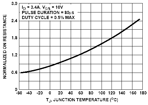
Continuous Drain Current . . . . . . . . . . . . . . . . . . . . . . . . . . . . . . . . . . . . . . . . . . . . . . . . . . . . . . .ID: 5.6 A
TC = 100oC . . . . . . . . . . . . . . . . . . . . . . . . . . . . . . . . . . . . . . . . . . . . . . . . . . . . . . . . . . . . . . . . ID: 4 A
Pulsed Drain Current . . . . . . . . . . . . . . . . . . . . . . . . . . . . . . . . . . . . . . . . . . . . . . . . . . . . . . . . . . IDM: 20 A
Gate to Source Voltage . . . . . . . . . . . . . . . . . . . . . . . . . . . . . . . . . . . . . . . . . . . . . . . . . . . . . . . . VGS: ±20 V
Maximum Power Dissipation . . . . . . . . . . . . . . . . . . . . . . . . . . . . . . . . . . . . . . . . . . . . . . . . . . . . . PD: 43 W
Linear Derating Factor . . . . . . . . . . . . . . . . . . . . . . . . . . . . . . . . . . . . . . . . . . . . . . . . . . . . . . . . . 0.29 W/C°
Single Pulse Avalanche Energy Rating . . . . . . . . . . . . . . . . . . . . . . . . . . . . . . . . . . . . . . . . . . . . . . EAS: 19 mJ
Operating and Storage Temperature Range . . . . . . . . . . . . . . . . . . . . . . . . . . . . . . . . . . . . . . . . . . TJ, TSTG: -55 to 175 C°
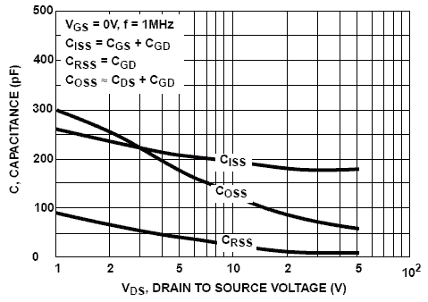
Input Capacitance . . . . . . . . . . . . . . . . . . . . . . . . . . . . . . . . . . . . . . . . . . . . . . . . . . . . . . . . . . . . f = 1.0MHz - 135 - pF
Output Capacitance . . . . . . . . . . . . . . . . . . . . . . . . . . . . . . . . . . . . . . . . . . . . . . . . . . . . . . . . . . . COSS - 80 - pF
Reverse-Transfer Capacitance . . . . . . . . . . . . . . . . . . . . . . . . . . . . . . . . . . . . . . . . . . . . . . . . . . . CRSS - 20 - pF
Internal Drain Inductance LD Measured From the Contact Screw On Tab To Center of Die . . . . . . . . . 3.5nH
Pulse Source to Drain Current . . . . . . . . . . . . . . . . . . . . . . . . . . . . . . . . . . . . . . . . . . . . . . . . . . . .ISDM - - 20 A
Source to Drain Diode Voltage VSD TJ = 25C°, ISD = 5.6A, VGS = 0V. . . . . . . . . . . . . . . . . . . . . . . 2.5 V
MOSFET specs:
. .

. 
Pictures of users who build the project
This is how Adrian VK3LK made it:
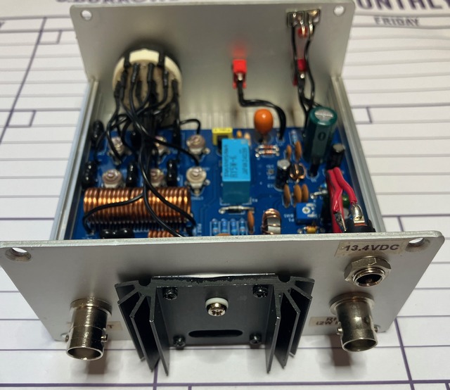
And he has the Gerber Files PCB for this project designed! Download Gerber Files for the PCB, made by Adrian VK3LK
Thank
you Adrian for all your work!
This is how John SV1ONK did it:
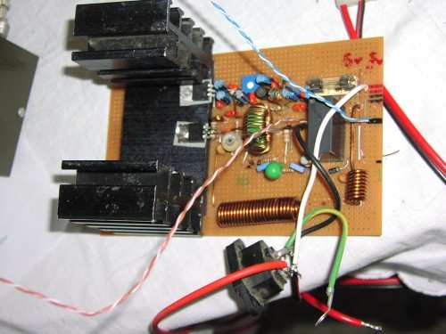
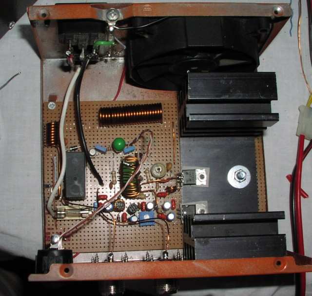
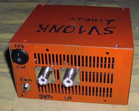
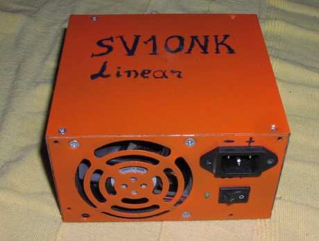
He made it for the 20-meter band.
Thanks John!
This how Konstantinos SV1ONW made it:
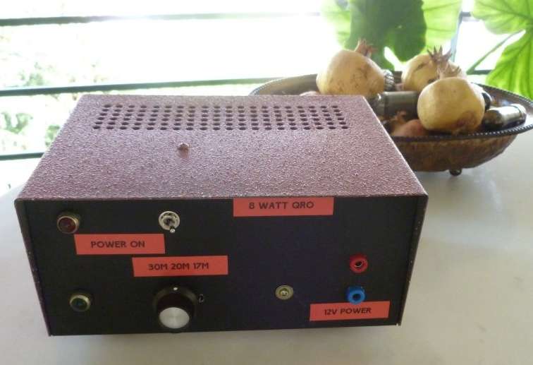

Thanks Konstantinos!
Little note on Antenna's
It's important to use a correct designed antenna according to band you would like to operate, or at least use a good antenna tuner to match the antenna (protecting your transmitter and proventing harmonics/interference...).
A resonant antenna
is an absolute requirement for QRP operation, and an amplifier is
not a "band-aid" for a poor antenna system!
We cannot expect good results from low levels of RF output if the
power gets wasted in lousy coax, corroded connections, or poor
antennas. Several examples can be found on my website and all
across the Web. A dipole is always a good alternative (total
length = 150 / freq - 5%).
Another
related project:
..15 & 17 meter band transistor 10 watt
amplifier
Remember that transmitting and/or using an power levels higher that your local license permit is illegal without a valid radioamateur license!