Classical Laboratory Power SupplyJanuary 2019 How it happenedMany years ago I made "laboratory power supply" - two times independent power supply 0.7 - 15 V/1 A with adjustable current limitation and additional power supply 5 V/1 A. Concept of the power supply was built on 723 chip, it worked quite fine for a years and survived a lot. It had no indication of output voltage or current, current limitation adjustment worked a bit roughly. And for a years it had only "temporary" hand made scales for voltage and current adjustments. This winter something happened with the device. Probably due to cold in the room its transformer started to be very noisy. Then it came D-day... Power supply concept based on 723 chip is still quite acceptable, moreover device is, more or less, completed. That means that after fixing transformer issue, adding output indicator to front pannel and fixing scales for output voltage and current the device would be back in life. But adding indicator to front pannel requires complete disassembly, because to do big hole on the front panel of the intact device is very risky. So, when device is already disassembled, why not to fix also that current limitation adjustment. Key idea I got making old lamp reconstruction. Battery charger is in principle constant voltage power supply with maximum current limitation. Schematics can be found in data sheets providers of chip 317. Very inspirative is National Semiconductor "LM117/LM317A/LM317 3-Terminal Adjustable Regulator" data sheet. Page 22 contains the following schematics: Simple charger schematics:
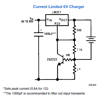
As it can be seen standard voltage regulator is extended by transistor and resistor. Current flowing through charged battery goes through sensing resistor. It results in occurrence of voltage on the transistor base. When it reaches value successful to open transistor, then transistor starts to decrease voltage at the adjustment input of the 317 chip which results in decreasing of output current. Transistor is used as inverting amplifier. It compares base opening voltage of transistor B-E junction with voltage on the sensing resistor. It seems, that for simple devices this approach is more than satisfactory. In case continuous adjustment of maximum output current would be required then use of this approach would be technically difficult. On the NET I found designs using switching of sensing resistors of different values. For charger it seems applicable, but not for laboratory power supply. It seems that problem of current limitation adjustment can be solved using real operating amplifier (OpAmp) in place of transistor.
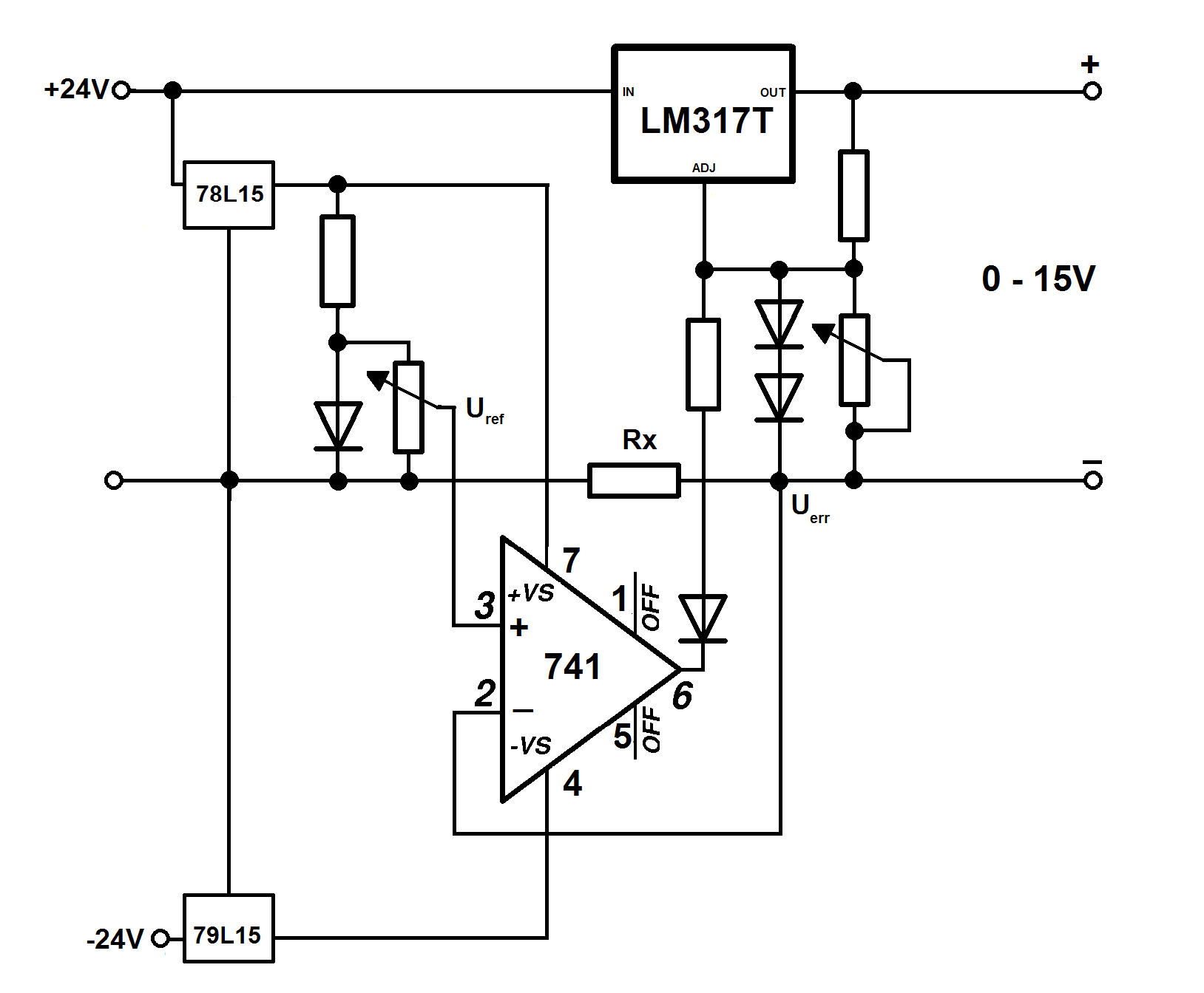
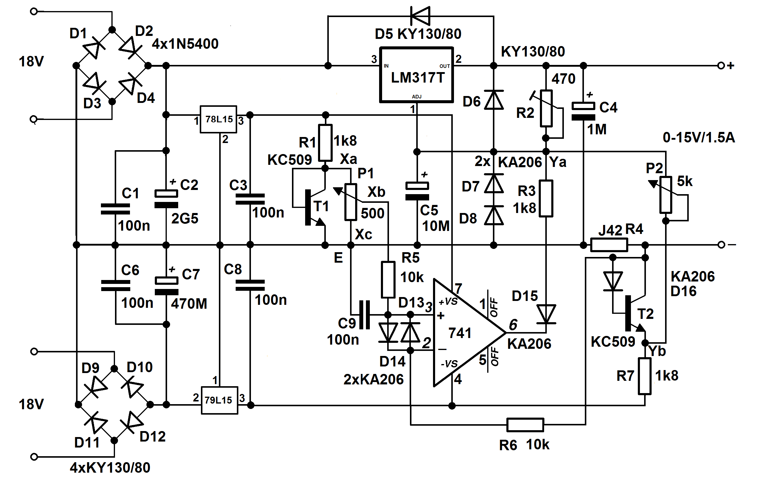
Replacement of transistor brings possibility to adjust current continuously using variation of reference voltage. It brings, however, complication in the fact, that OpAmp requires also negative voltage power supply. This will, however, bring also advantage - output voltage can be set from zero Volts. Classical approach to add negative voltage power supply to the design would be to add additional section to transformer (or add additional transformer). This section (transformer) doesn't need to be very powerful - current consumption of OpAmp is just couple of tens of mA. Modern approach would be to use voltage converter. I decided for classical approach using additional small transformer (for now). Source of low voltage reference can be made using diode. Classical silicium diodes give voltage around 0.65 V, Shottky diodes, dependent on model, around 0.25 - 0.35 V. More slopy V-A curve can be achieved using transistor having collector connected with base. It gives around 0.63 V, in case additional silicium diode is added to base then voltage is approximately doubled. Resulting schematics is based on above principal one and it contains suggested components to prevent damage both 317 and 741 chip as well. Also voltage adjustment from zero is added.
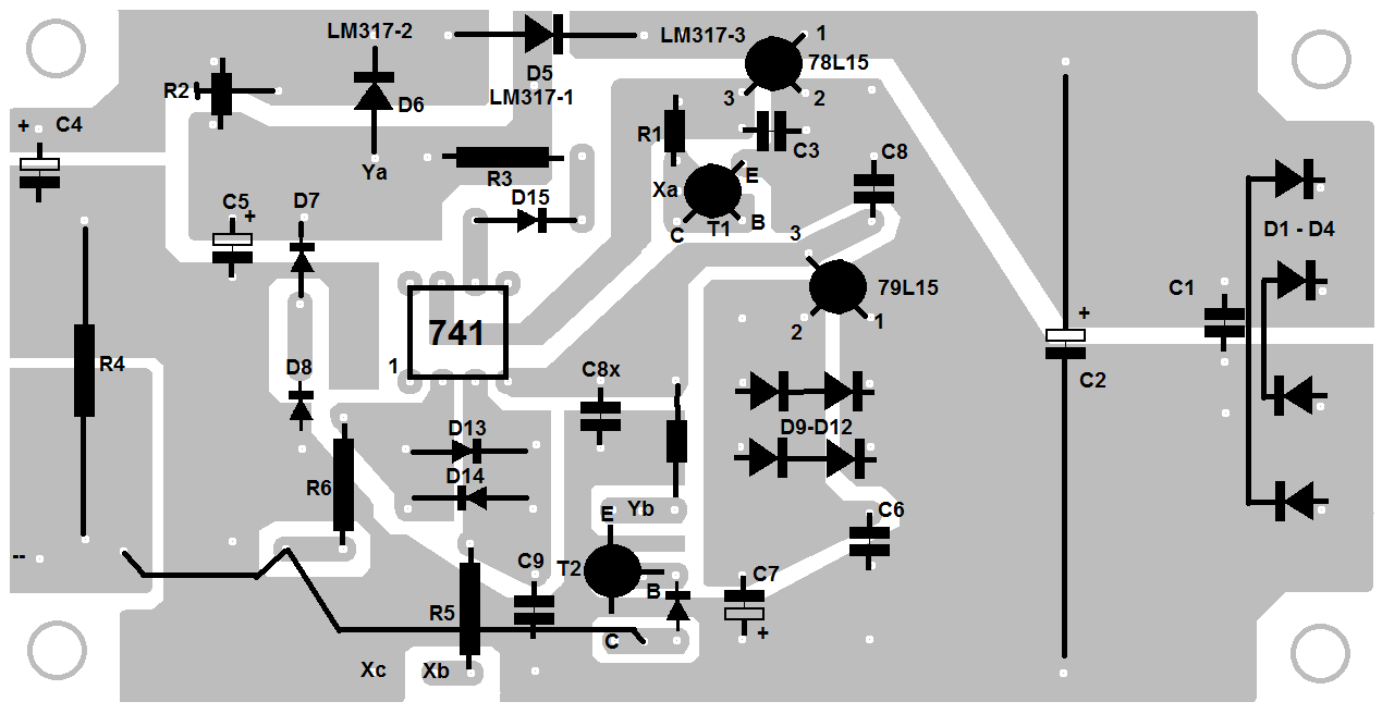
is using one side plated material. It has dimensions 55 x 107 mm (picture is in 300 dpi). LM317T is not mounted on the PCB - it is mounted on the rear side cooler plate. To prevent instability two identical condensers 100 nF are soldered directly on the pins - between input and ADJ and output and ADJ. They should be for 40 V or more.
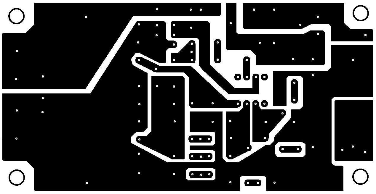
has no problems as it was designed for classical components. Comparing to schematics there is one additional condenser 100 nF (C8x) as there was just a piece of free space. It is not necessary to use it. Output electrolytic condenser C4 is soldered from bottom side of the PCB (if bigger type is used). Points to connect LM317T wires are marked as "L7317-1", "L7317-2" and "L7317-3" where last digit is a pin number. Points to connect potentiometer P2 5 k to set output voltage are marked "Ya" and "Yb". Maximum voltage is adjusted using trimmer R2 when P2 is set to maximum. Points to connect potentiometer P1 500 (470) Ohm to adjust maximum current are marked "Xa", "Xb" and "Xc". Maximum current is basically set by adjusting of sensing resistor R4. It was wound using wire from old resistor. Such a small resistances are difficult to measure using standard multimeters. It requires to use A-meter, V-meter, power supply and some small car bulb (to limit current). Real resistance value is calculated using Ohm's law. It was also tested constantan wire from heating spiral. It worked, but it was impossible to solder. In case somebody would decide to create required resistance using parallel combination of bigger resistors it should be taken into consideration, that maximum power dissipation is close to 0.7 W. Required value of R4 is calculated from reference voltage value (0.63 V) and maximum current required (1.5 A) using Ohm's law: 0,63/1,5 = 0,42 Ohm In case final resistance would be bigger that required it will be impossible to set maximum current value. It should be mentioned also, that LM317T alone has built in limitation of output current (about 1.5 A). In result maximum output current will be result of interaction of both those adjustments. It should be mentioned that rectifier diodes D1 to D4 and D9 to D12 are mounted vertically and connecting points for power wires are in fact "in air". Diodes 1N5400 are for maximum current 3 A. In case they would be permanently doing that it would be necessary to solder both wires to PCB for cooling. Power supply in design has not such an ambitions so it is safe to mount diodes vertically which saves some space. Filtering electrolytic condensers C2 and C7 must be dimensioned for peak voltage from transformer. If 15 V output voltage is considered then minimum AC voltage must be about 18 V. In that case condensers must be for at least 18 x 1,414 = 25,5 V. In case of higher AC voltage they must be dimensioned proportionally higher.
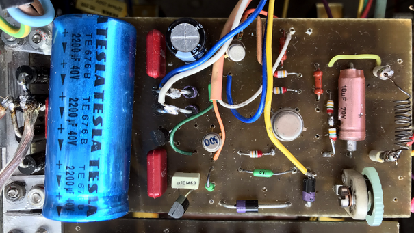
Prototype view.
SummaryThe goal of this project was to get pleasure from reviving things which otherwise would end up in litter. On the market there are good quality laboratory power supplies for acceptable price, so commercial part of this project is not considered. Additionally in case it would be necessary to buy all components then the whole project would not have too much sense. Switching power supply as a source of negative voltage for OpAmp is still option to simplify design. Similarly to battery charger also here is real option to use cheap commercially available charger in place of negative voltage source. Note, that it is not necessary to serve OpAmp full 15 V. Much lower negative voltage, say 5 V, could be quite enough. In that case diodes D9 to D12 as well as 79L15 could be excluded from the design and it will be enough to decrease R7 value proportionally to voltage. Another possibility could be to design small dummy switching converter serving enough negative voltage power (more that 8 V) and replacing 79L15 by smaller voltage type.
This is |