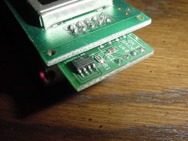
MCT-III is just like the MCT-II except that it has an audio amplifier with sine wave output, an 8 ohm speaker, a 3-AA cell battery pack, and 3.3V regulator. The "a" version requires you to solder the 20 pin TSSOP package and the Audio Amplifier SOIC.
The MCT is set up for the convenience of the operator in four different sections:
- Trainer Mode � This section is setup for the new person to Morse code. First, it introduces them to numbers
and characters sounds, then quickly moves them to hearing the word sounds of the characters just learned, and
learning how to send those word sounds. How to set up and use the new paddle for learning Iambic characters,
and Mode �B� sending. Just like in the practice sessions but the word groups in each session are made up of
characters just learned.
- Practice Mode � This section is setup for the experienced CW operator who would like to increase their
skills and proficiency, by learning word sounds and how to send words sounds correctly. It contains a library
of over 1,000 words and Ham abbreviations, from single a letter to seven letter words. It�s setup to help
the operator quickly reach that point of hearing the music of CW, and copying in their head!
- General Setup Mode� These are the unique functions that support both training modes and makes the
difference in helping the new ham enhance their skills quickly without all the pit falls and plateaus encountered
in the past when learning this language.
- Iambic Keyer Mode � This is, as the user will soon come to realize, the finest sending devices on the
market today. With its easy to use responsive keyer, always knowing at what speed the device is set to while
sending, and eight (8) memories with a capacity of 128 Characters per memory with imbedded feature to repeat
a memory and or Link memories together, will surely meet any requirements.
Features:
- - OLED 4 lines Display of Menu items, Memory, Functions, etc.
- - Low current drain (MCT-I)
- - Selectable A/B Keying
- - Adjustable WPM sending (5 � 100 WPM)
- - Adjustable TONE (100 � 4000 Hz)
- - Adjustable PAUSE between Words (0-5000mS)
- - Adjustable WORD LENGTH (2 � 7 letters + ALL)
- - Adjustable REPEAT of words (1 � 50)
- - Adjustable TRAINING WORDS (10 � 300)
- - Trains the beginner how to Adjust a Paddle
- - Trains the beginner how to SEND Iambic characters
- - Trains the beginner in WORD SOUNDS
- - Trains the beginner in an easy way to learn NUMBERS
- - Trains the beginner how to SENDING WORDS
- - Trains the seasoned ham in WORD SOUNDS (head copy)
- - Trains the seasoned ham in SENDING WORD SOUNDS
- - Eight (8) Programmable Non-volatile MEMORIES (5 on the MCT-I)
- - 128 Character Memory Capacity per memory
- - Adjustable Imbedded commands for Memory DELAY (1 � 9 Seconds) (Beacon Mode)
- - Imbedded commands to LINK or LOOP memories together
- - MEMORY PROGRAMMING via Paddle input
- - ON DEMAND memory editing
- - Saved memory ERROR CORRECTION
- - Complete memory DELETION
- - Smooth and responsive KEYER
- - Detailed User and Assembly manual
The team had a Farnsworth timing discussion to decide whether to implement it or not on the MCT. The ARRL adopted it based on future higher speed code training (their opinion). However, the whole purpose of our MCT is to improve "WORD
sound" recognition. Along those lines, practicing receiving/sending at 10WPM allows you to send regular 10WPM words after receiving the selected word (.....for "n" times). The word being received with Farnsworth timing means 18WPM characters with larger spaces to make the overall word speed 10WPM. The problem with that is that those two words (received and sent) will not "sound" the same and negates the unique MCT training effect.
Since the device is small and runs on batteries, it�s perfect to take anywhere to continue practice during those business trip evenings to work on enhancing ones skills.
"The Kit" is one of Amateur Radios best features called Home Brewing. To some this it�s the best part of the
hobby, but one that is not practiced much anymore by the new comers or Old Timer. It used to be a large part
of the hobby and gave a person the thrill and experience of building something with their own two hands and
sharing it with others on the air.
The MCT-I and MCT-III Kits don�t take a lot of time to build, and it�s a great learning device for first time SMT builders. ALL the kits use the same level of firmware running on the same LPC824
microcontroller.
To support the requirements of the various builders, ALL the kits will now be supplied with 7mm (short) tactile
switch levers ---AND--- 13mm (tall) tactile switch levers. You decide which ones you want to use on your kit.
-------------------------------------------------------------------------------
KIT PRICES:
--------------------------------------------------------------------------------
Enclosures are up to you to source from the various suppliers....for Example:
- Hammond RL6215......125mm x 80mm x 35mm, has 4 screws for lid
- Hammond 1591BSGY....112mm x 62mm x 27mm, has 4 screws for lid
---------------------------------------------------------------------------------
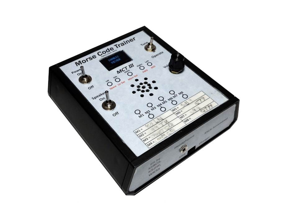
Example of a MCT-III in a SERPAC A31 enclosure, showing qty 13 of the 13mm tactile switches with overlay "domed"
over the pushbuttons.
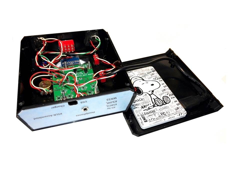
Inside of above MCT-III in a SERPAC A31 enclosure.
The Attenuator Kit #13
THESE KITS ARE IN STOCK
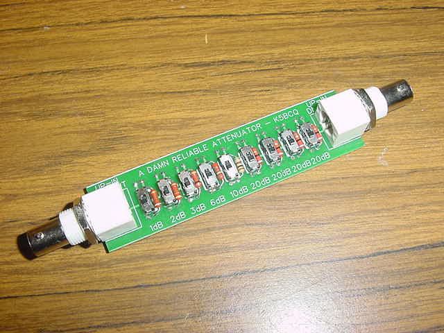
The assembled Attenuator Kit showing the front side and mounting of the
resistors.
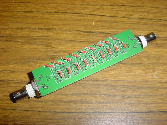
The assembled Attenuator Kit showing the back side and mounting of the
resistors.
This was developed as a crude but simple HF Attenuator after I had miserable reliability problems
with commercial attenuator switches. The attenuation would change depending on how the switches
"felt" that day. Very difficult to get repeatable results. I also tended to stress the attenuator
resistors because of their 1/4W rating. This kit provides Vishay 1W 5% resistors and uses jumper vs
switches. Sure, they makes it a little more time consuming to change values, but the jumpers provide
very positive contact and if they wear out .....get another jumper, they only cost 1 cent each and
extras are included in the kit. Due to the "Open Design", I would not use this above HF frequencies.
It has served my needs, does what I need an attenuator for, and will work for you too.
The kit can be provided with BNC connectors as shown or SMA board edge connectors. Your choice to
specify, same price.
The jumpers are a little cumbersome if you change them often so we ---HAD--- an option to replace
the 9 2x3 Headers and 25 Jumpers with 9 slide switches for an additional $x.00. HOWEVER, the newer
100mil pin spacing switches from China have proven to be unreliable relative to contact resistance
and that option has been pulled. Earlier "Alco" switches were fine but I can't find them anymore.
Ben Bibb, NO5K, checked this Attenuator in his lab and was very impressed. The SWR at 6m is only 1.2
and the SWR at 2m is only 1.4. Lower frequencies are, of course, better with a SWR of 1.0 to 1.1. Ben also
found the accuracy of the attenuation to be within 1-2% and the Return Loss levels are very acceptable.
Insertion loss is a fraction of a dB. Those 1W Vishay 5% resistors are good ones and cost $0.18 each.
Overall not bad for a $15 open board Step Attenuator.
So what comes in today's Attenuator Kit ? ......Bill of Material:
- 1 PC board
- 2 SMA or BNC connectors
- 9 2x3 headers with 25 Jumpers --or-- 9 slide switches
- 2 Vishay 1W, 5% 910 ohm resistors
- 2 Vishay 1W, 5% 430 ohm resistors
- 2 Vishay 1W, 5% 300 ohm resistors
- 2 Vishay 1W, 5% 150 ohm resistors
- 4 Vishay 1W, 5% 240 ohm resistors
- 2 Vishay 1W, 5% 100 ohm resistors
- 8 Vishay 1W, 5% 62 ohm resistors
- 1 Vishay 1W, 5% 75 ohm resistor
- 1 Vishay 1W, 5% 36 ohm resistor
- 1 Vishay 1W, 5% 18 ohm resistor
- 1 Vishay 1W, 5% 12 ohm resistor
- 1 Vishay 1W, 5% 5.6 ohm resistor
The price for the Attenuator #13 is $15 plus $4 postage in the USA and $13.85 postage for DX.
The 5W HF Amplifier Kit #21
THE PARTIAL KIT IS PRESENTLY IN PRODUCTION, 5 PARTIAL KITS IN STOCK
PC Board ONLY is available for $10 which includes postage in the USA.
Since I keep receiving requests for this kit (it's a really good and very useful 5W Amp design) and I don't
know when I will be able to get back to kitting more up......I have decided to make a Partial kit with all the
more unique parts .....and the heatsink available for $30 plus $4 postage in the USA.
So what comes with this Partial 5W Amplifier Kit #21 .......
- 1 Double sided board with silkscreen and soldermask, the board measures 1-3/8" X 2-3/8"
- 1 Schematic and Bill of Material for above board
- 1 RD06HHF1 MOSFET
- 1 OMRON G6H-2F RF Relay
- 1 KA78L06A 6V Regulator
- 1 FB43-101 Ferrite Bead
- 1 BN43-202 Binocular Ferrrite Core
- 1 BN43-2402 Binocular Ferrite Core
- 2 FT37-43 Ferrite Cores
- 1 249pF mica 500V Capacitor
- 1 10Kohm Potentiometer
- 1 Heatsink from HeatsinksUSA
You will have to source the rest of the parts based on the Bill of Material listed below and do any heatsink
drilling yourself. Should not be a problem for most Homebrewers.
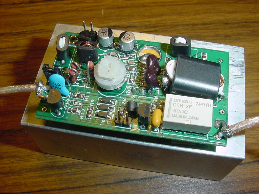
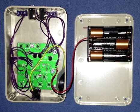
The 5W HF Amplifier shown with the new optional Heatsink. The SMA connectors were installed for my testing,
the kit is provided with 50 ohm coax to connect to the BNC/SMA/HF connector of your choice. Normally the Ampifier
would be mounted in an enclosure with a hole so the MOSFET can be bolted directly to the outside heatsink.
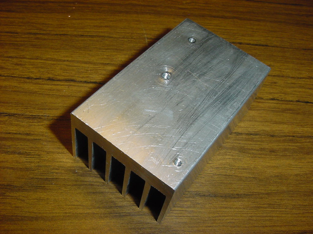
Picture of the optional drilled and tapped heatsink.
It would be nice to have an Amp with a little less power than the 20W amplifier Kit #15, so here is a 5W
version using a single MOSFET with an optional drilled and tapped heatsink (no fan required) from HeatsinksUSA.
When it comes to Amplifiers, the Radio Amateur is responsible for making sure his amplifier operates
within the guidelines established by the FCC and that it does not cause unwanted ipassnterference. This is
a Broadband Amplifier and will require some sort of Low Pass Filter (LPF) or Band Pass Filter (BPF) on
the output to attenuate harmonics. You may already have one you intend to use.
My idea was to provide a good and low cost Amplifier for the HF bands (160m to 6m) which can be
driven by a SoftRock SDR or any other low power driver and provide ~20dBm of gain. Low power being
defined as ~100mW. Some of the new SDR units supply less than 50mw and really need a little �boost�. This Amp uses
the RD06HHF1 RF MOSFET which are rated at 6W output for 12.5VDC at 30+MHz. These parts
are quite robust and much better than the IRF510 Switching Power Supply MOSFETs used earlier, largely
because of their low cost and availability. The other advantage of the RD06HHF1 is that the mounting
tab is attached to the �Drain� pin which is at ground potential �so no mica insulator is required.
Just like the 20W HF Amplifier Kit #15, this Amplifier has a Signal Operated Switch (SOX) for CW QSK. I
didn�t really put it there for SSB �..but who knows (still better to use PTT). Did I mention good and low cost ?
The design and components which have been selected require that the operational criteria of 1) an
Input of ~100mW �AND-- 2) an Output of 5W max ���whichever comes first, NOT be exceeded. To allow
some adjustment, the input to the Amplifier has places for a Pi network Input Attenuator of your
selection (Rx, Ry, Ry) �.3dB, 6dB, etc. Parts for a 3dB (50% power reduction) attenuator are provided
in the kit. The purpose of the attenuator is to reduce input power and to provide proper 50ohm matching
for the driver. This design has been extensively tested and optimized to provide good matching to 50ohms
without the attenuator. If you elect to not use an attenuator, replace Rx with a jumper and do not
install either Ry.
The design also provides Class C operation (CW only). This allows lower power consumption when you
really don�t need linear operation. The Gate Bias current on the MOSFET is set to around 20mA with the
potentiometer if you prefer and only want to run Class C (for CW)....much less heat generated.
Many MOSFET Amplifier circuits do not use a feedback circuit but I thought it would be good design
practice to do so and added one. The T2 compensation capacitor is a 249pF Mica capacitor. This value
seems to work best for 160m to 6m (emphasis was put on working well at 6m), and Mica capacitors are very
stable across a broad range of frequency and temperature.
Another design parameter which seems to help on all the bands, especially 6m, is to further reduce
spurs by paralleling capacitors of different values to reduce the capacitor self resonance effects. You
will see that in many cases a 100nF cap is in parallel with a 47nF cap or 10nF cap and also a 1nF cap.
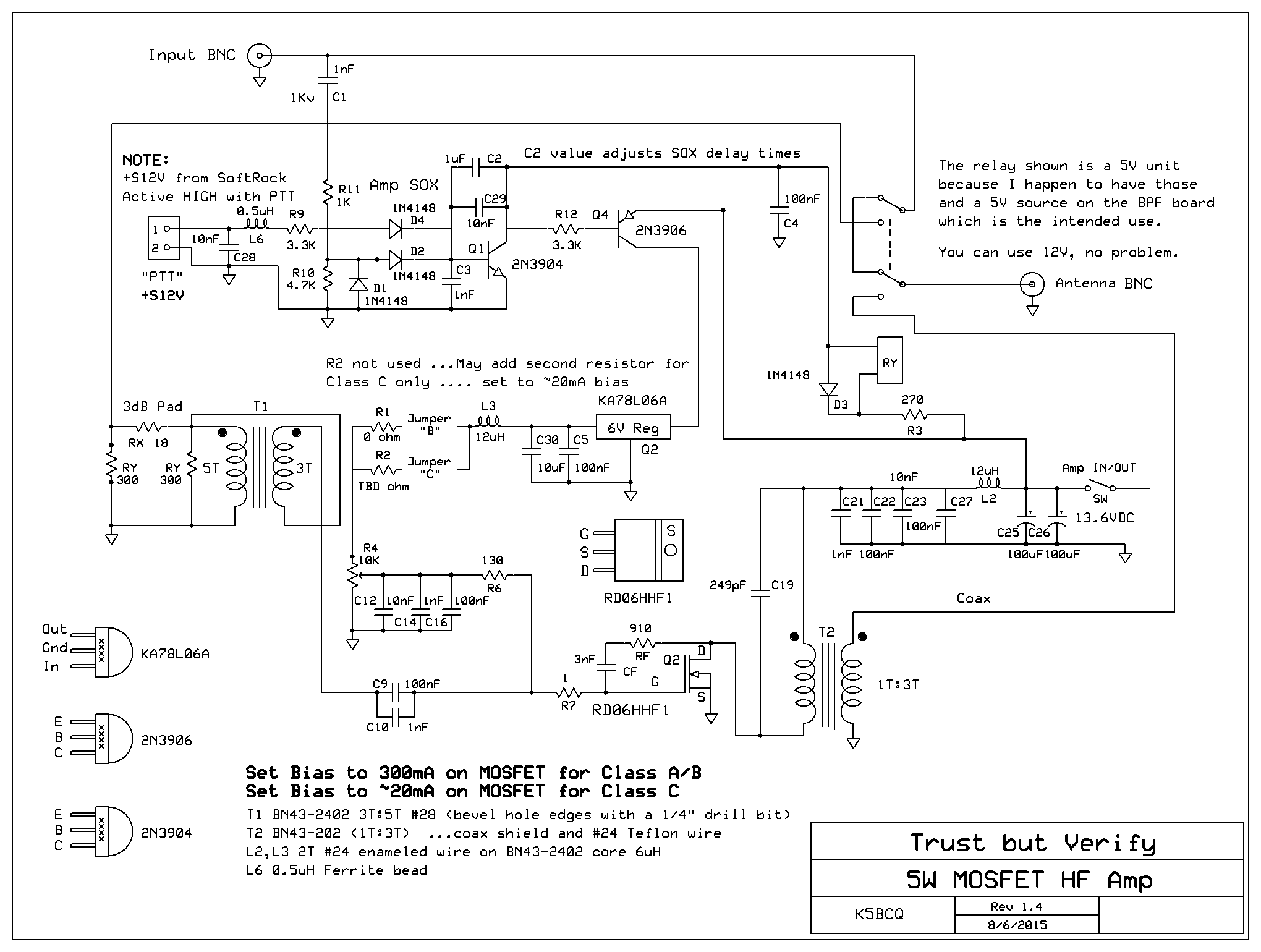
Here are the assembly Instructions for the 5W Amplifier
5W Amplifier Construction Hints
5W Amplifier Schematic
-----------------------------
ERATTA: For the current level V1.0 board and Rev 1.4 schematic.
- There is a footprint on the board for C24. This capacitor footprint is not populated and not shown
on the schematic. I decided it was too close to the FET mounting hole.
- C6 is a 10uF capacitor provided on the Bill of Material. This capacitor is no longer used and not on
the schematic.
-----------------------------
So what comes in today's 5W amplifier Kit ? ......Bill of Material:
- 1 Double sided board with silkscreen and soldermask, the board measures 1-3/8" X 2-3/8"
- 1 Schematic and Bill of Material for above board
- 1 RD06HHF1 MOSFET
- 1 OMRON G6H-2F RF Relay
- 1 KA78L06A 6V Regulator
- 1 FB43-101 Ferrite Bead
- 1 BN43-202 Binocular Ferrrite Core
- 3 BN43-2402 Binocular Ferrite Cores
- 1 2N3904 NPN Transistor
- 1 2N3906 PNP Transistor
- 4 1N4148 Si Signal Diodes
- 1 249pF mica 500V Capacitors
- 2 33uF Electrolytic Capacitors
- 2 10uF Ceramic Capacitors
- 6 100nF Ceramic Capacitors
- 3 10nF Ceramic Capacitors
- 1 1nF 1KV Ceramic Capacitors
- 4 1nf Ceramic Capacitors
- 1 1W 270ohm Vishay Resistor
- 1 1W 130ohm Vishay Resistor
- 1 4.7Kohm Resistor
- 2 3.3Kohm Resistors
- 1 1.0Kohm Resistors
- 1 0 ohm Resistor
- 1 10Kohm Potentiometers
- 1 3nF FB Capacitor for the feedback loop
- 1 910ohm FB Resistor for the feedback loop
- 1 1W 18ohm Vishay Resistor...really nice small 1W resistors
- 2 1W 300ohm Vishay Resistors....really nice small 1W resistors
- Various braided wire, enameled wire, bifilar wire, coax, headers
I offer two heatsink options:
#1) No Heatsink, Just the 5W Amplifier for $35, you come up with your Heatsink
#2) A 4.23" x 2.90" x 1" Heatsink from HeatsinksUSA. This Heatsink has 1 hole drilled and
tapped to match the MOSFET and 2 mountin holes. I am the driller/tapper. Price will be an additional $5. Postage will go up
because of the added weight.
Shipping for one kit with option #1 (NO heatsink) is $4 First Class Mail in the USA and $9.50 First Class
Mail for DX. Shipping for a kit with Heatsink option in the USA will be $6. DX shipping costs are
determined by location.
The AQRP 8KHz to 440MHz Vector Impedance Analyzer kit #25
THIS KIT (AND BOARD) ARE SOLD OUT. PRODUCTION OF THE NEW VIA-II USING THE STM32F746G DISCOVERY TBD.
Several units have been distributed locally for testing and it looks good.
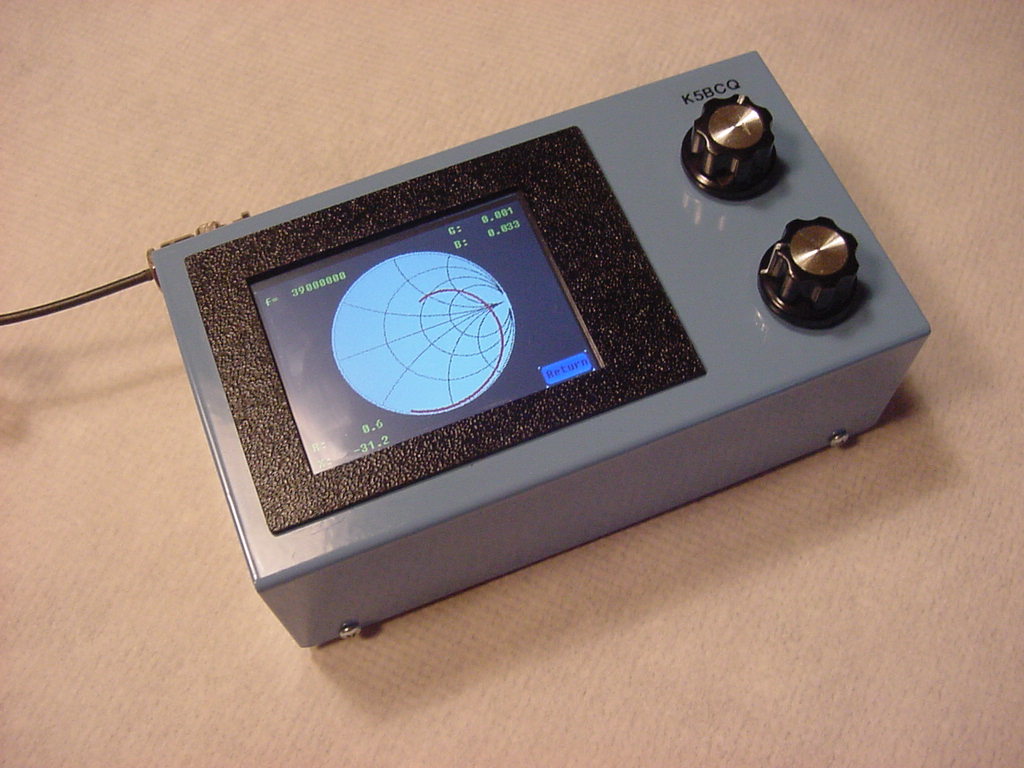
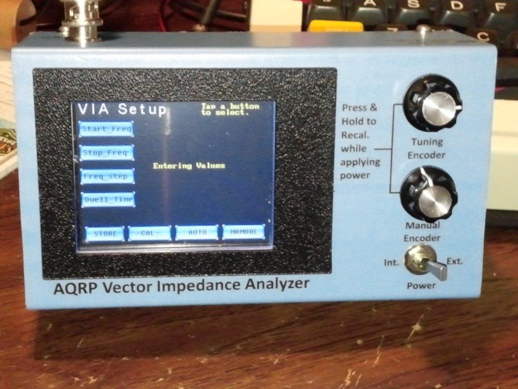
An assembled AQRP VIA showing a Smith Chart. It can also plot parameters across a range
you define and can provide parameter data screens
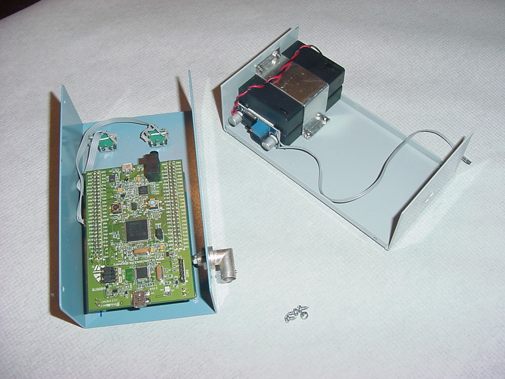
Shows the 3 board stack using the STM32F407-Discovery board. Programming updates are
via the USB connector to your computer. Two, 3 cell each, battery packs are shown.
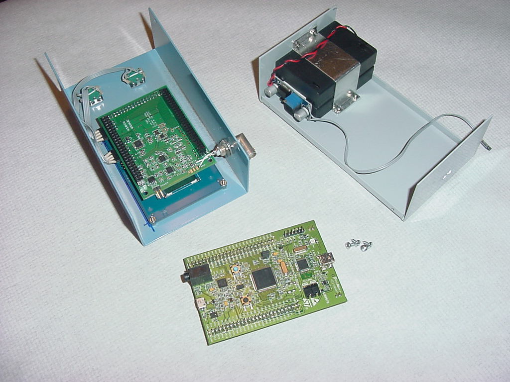
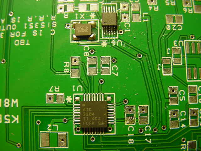
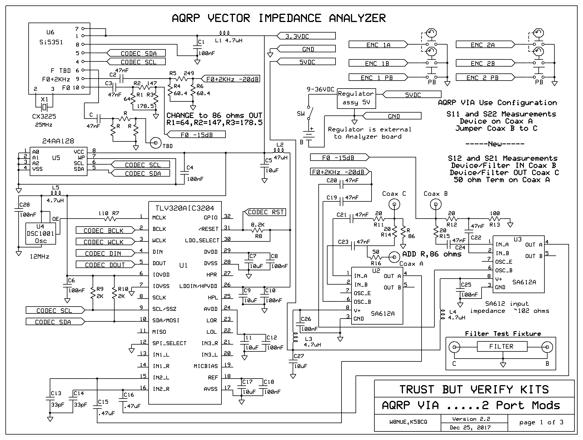
Shows the VIA board with the RF bridge, attenuators, dual SA612A mixers, audio CODEC,
Si5351A frequency control, memory, and interface to the TFT Display and
STM32F4Discovery board.
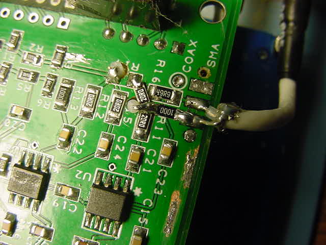
Shows the 2-Port rework on the board with the coax center conductors coming from the back and
through the VIA board. See the rework instructions for more detail.
The STM boards being shipped with the VIA kits today are all "C" level boards and are marked
"MB997C" on the silkscreen and "MB997 C-01" on the sticker. These boards have the Microcontroller
(U4) programmed with the latest level VIA firmware.
It has come to our attention that people sourcing their own STM32F407G-DISC1 boards from
Farnell, Mouser, and others may receive a "D" level STM board marked "MB997D" on the
silkscreen and "MB997 D-01" on the sticker. Early versions of the "D" may have a problem.
It manifests itself after you load the VIA code using the USB port (CN1) and switch to
external 5V power ......the system hangs and just sits there.
Easy to fix ......use the STM32 ST-LINK Utility (which you used to load VIA firmware into U4)
to also load new firmware into U2. Select "ST-LINK" and "Firmware Update" ....level V2.J27.S0
or V2.J27.M15 will fix the problem and you're good to go.
******************************************************************************
Milt Cram, W8NUE, and I decided we wanted to use some of the great development kits out there
which are available from various manufacturers at VERY reasonable prices to entice users to
design and write code to use "their" products. This coupled with "free" Development Tools is
an easy sell for us. The STM32F407-Discovery boards have plenty of microcontroller capability and
features.
Milt drew on his SDR2GO firmware experience, firmware he used for the NUE-PSK Digital Modem,
and also the more recent STM32-SDR code. He decided to base the design on using audio baseband signals
and process those for the required data.
The inexpensive Si5351A proved to be ideal and we run two of the three outputs, separated by 2KHz,
into dual Synchronous Detectors/Mixers (SA612As low noise, mixers). Harmonics and much of the potential
adjacent interference signals are not a problem due to using Synchronous Detectors. The VIA works by
making U2 a Current Detector and U3 a Voltage Detector. Measuring Current and Voltage (level and phase)
provides all the imformation needed for the various S11/S22 parameter measurements. Device Under Test
(DUT) connector impedance 0f 50 ohms is not required because both Current and Voltage (and phase) are
being measured. The two baseband signals are fed into a great little CODEC we've used on several
projects with good luck. The digital info is sent to the STM32F407 microcontroller for processing,
storage, and display. We haven't decided what to do with the third RF output from the Si5351A).
Ongoing experimentation for a 2-Port S12/S21 upgrade kit has met with success and a 2-Port kit of
parts is now included with every new VIA kit sold. The kit is available to upgrade existing VIAs.
After looking at several display possibilities, we decided to go for something large and user
friendly .....and here we have it; The AQRP Vector Impedance Analyzer kit #25. The AQRP VIA has the
unique advantage of being able to readily process negative complex numbers correctly .....a problem
with many mid range commercial antenna analyzers out there.
It's a standalone, battery powered, Vector Impedance Analyzer for portable operation. Can be
used to check antennas, filter designs, etc, etc. This design will evolve over time as changes and
improvements are made to function and visual presentation. The STM board firmware is easily
updated by using STM-LINK software (free) and a USB cable.
HELPFUL DOCUMENTATION:
AQRP Vector Impedance Analyzer Operations Manual V1
AQRP Vector Impedance Analyzer Operations Manual V2
A Note on Changes to VIA Operating Instructions
Instructions for AQRP VIA Data Transfer to your PC for further analysis
AQRP Vector Impedance Analyzer Data Transfer to PC - Example
AQRP Vector Impedance Analyzer Data Transfer ZIP File
AQRP VIA V2.x Firmware Notes
AQRP VIA V1 Construction Hints
AQRP VIA Battery Voltage Monitor implementation
AQRP VIA Troubleshooting Tips
AQRP VIA TFT Display Continuity Checklist
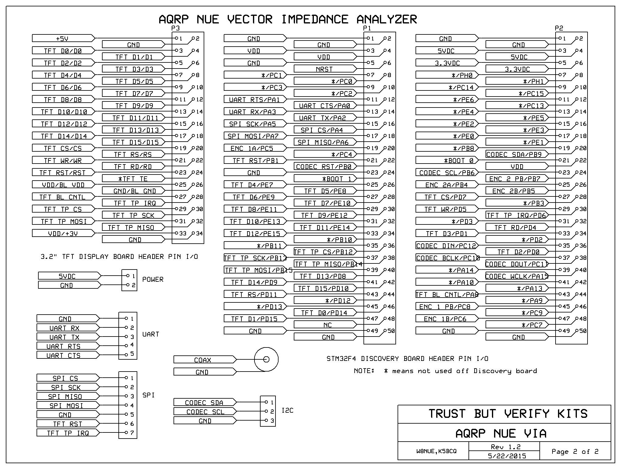
AQRP VIA Schematic, page1
AQRP VIA Schematic, page2
AQRP VIA Schematic, page3
AQRP VIA Schematic showing 2 port rework
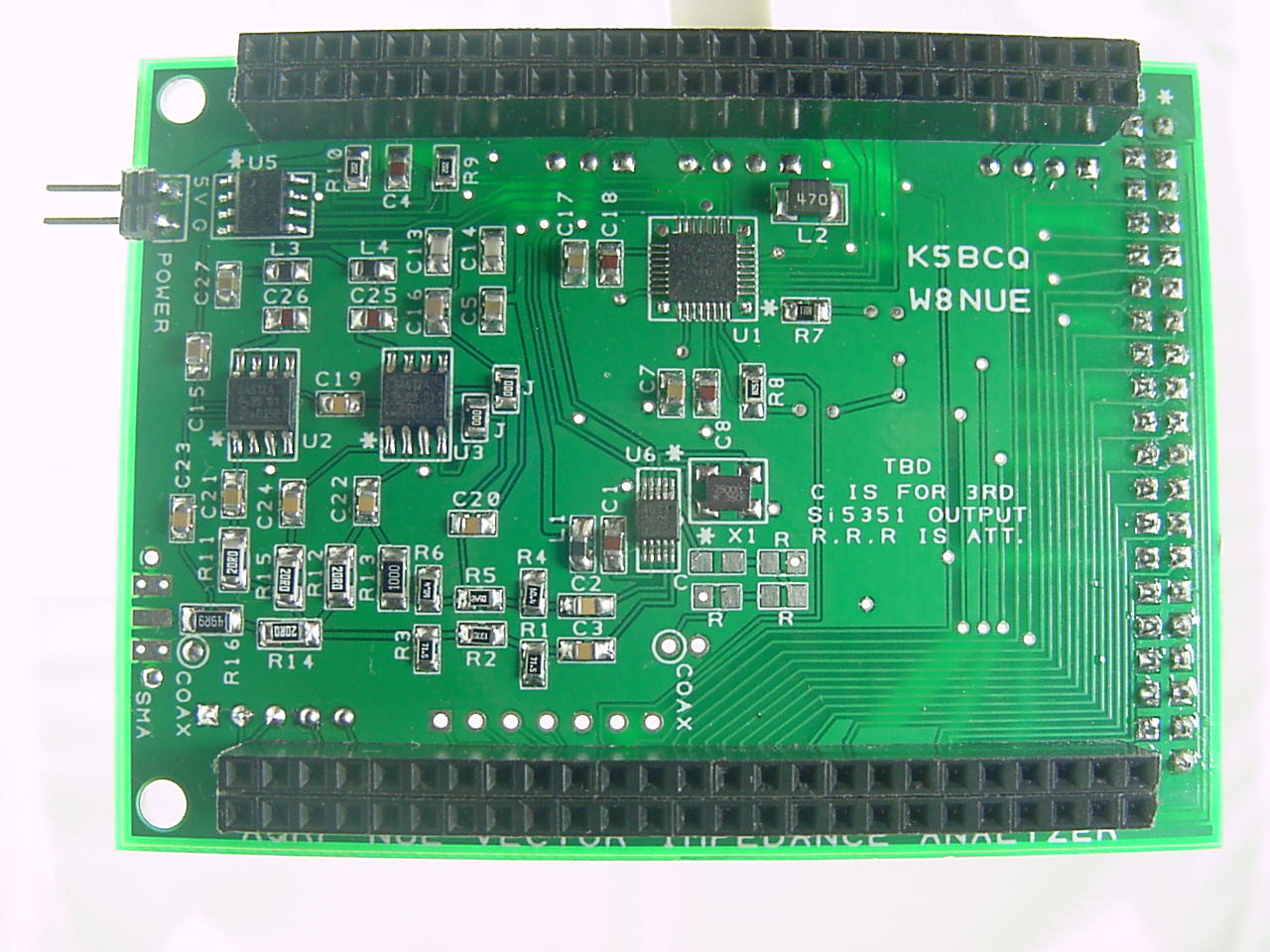
AQRP VIA board higher resolution of top
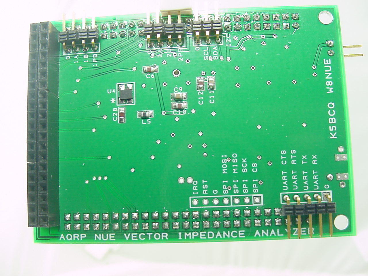
AQRP VIA board higher resolution of bottom
AQRP VIA Face Plate Over Lay for LMB Heeger CR-632 Enclosure
....PowerPoint file
AQRP VIA: Using an Uncalibrated Frequency Sub-Range
AQRP VIA: Small Transmitting Loop Antennas � A different perspective
on determining Q and efficiency
AQRP VIA 2-Port Modification Instructions
----------------------------------------------------
DESIGN FEATURES: (Firmware Ver. 2)
- Measures V (voltage) & I (current)
- Calculates Z (Impedance....in complex numbers), Y (Admittance....in complex numbers), k (Reflection Coefficient)
....in complex numbers, RL (Return Loss...in dB), VSWR (Voltage Standing Wave Ratio)
- Plots Z, Y, k, RL, VSWR, and Smith Chart (Reflection Coefficient Plot). Z and Y are complex number plots.
At the completion of a plot, you can choose to rescan using the same plot type, or to change the plot type.
The latter choice, allows you to select a different plot of the data that was gathered during the initial plot.
- Vertical line cursor on all x,y plots, showing the frequency and the corresponding plot values at the
location of the cursor.
- Smith Chart cursor--cursor follows encoder change along the plot, displays frequency, reflection coefficient, and VSWR.
- The default HF mode Frequency Range of the data/plots is from 1 to 440 MHz .....an alternative LF mode Frequency
Range is from 8KHz to 1.17MHz (1.17MHz is Fmax/128 which is a Si5351 constraint). Yes, all the way down to 8KHz.
A set of preset bands is also available from which to choose. Selecting the band will also set the corresponding
start, stop, and step values.
- Auto Scan and Manual Scan modes
- Adjustable Start & Stop Frequencies in Hz, Frequency Step in Hz, and Dwell Time (in msec to allow sufficient
data processing time).
- All parameters are saved on command for the next use
- Stores up to 1,500 data points with associated parameters for later PC Processing using a 512K EEPROM.
- Powered by six AA batteries and a 5V Switcher Power Supply. The DC-DC switcher will accept an input
of up to 30V DC. When using battery packs it is often desirable to measure the actual battery pack voltage. The VIA kit is supplied with 2 axial lead resistors (10k and 68k ohm) to form a voltage divider for the STM32F407 ADC. The 68k ohm is connected between the battery and pin PC1 of the Discovery board and the 10k resistor is connected between pin PC1 and the nearest ground.
- You may also use another power source (e.g. LiPo) if you want. There are many LiPo "Power Banks"
available for less than $10. Most of these contain a buck-boost regulator that allows a 3.7V Lithium Polymer
1800-2000 mAhr battery to be charged from a 5 V charger (as is used in most cell phones) and produce a 5V
regulated output that can power the Discovery board directly. WARNING...WARNING: YOU HAVE READ ABOUT
SOME OF THE CONCERNS OF USING LiPo BATTERIES, PLEASE PAY ATTENTION TO ANY WARNINGS ON THE BATTERY PACKS.
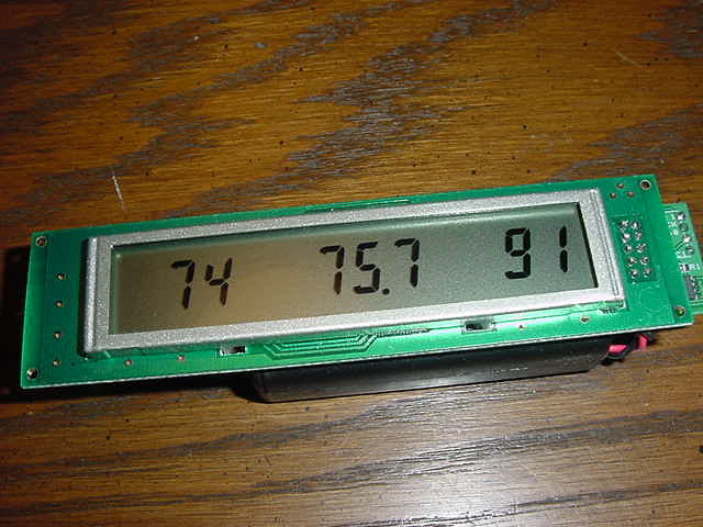
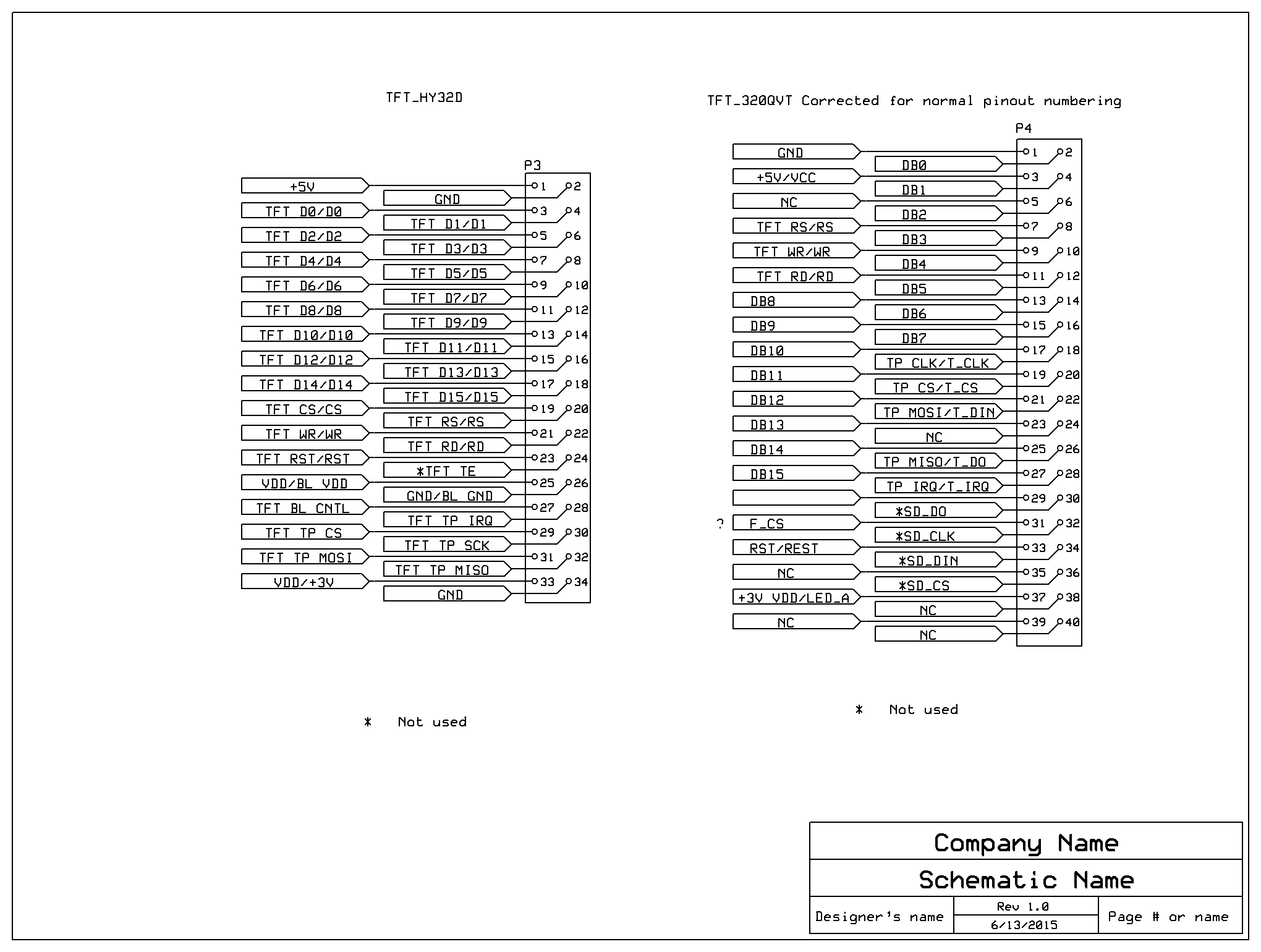
- Uses a TFT_320QVT display which is 320x240 pixels, color, and has a resistive touchscreen for parameter
selection. These are readily available on eBay.
- New Firmware can be easily installed using a USB cable connected to a computer. A free utility from STM
is used to download the firmware from the PC and install it in the VIA.
- Data stored in the VIA may be sent to a computer for further processing. A standard USB cable may be used
for this purpose. As noted above, this data may also be re-plotted within the VIA. This facilitates plot
selection within the shack, after recording data taken remotely at the antenna.
- Calibration data (Open/Short/Load) is captured and recorded for all frequency steps between Start and Stop
Frequency. This allows data to be recorded at the end of a transmission line, effectively eliminating the
coax from the computed and displayed data. These data values are sent to the PC when requested.
- Also included is the capability to change the value of the target characteristic impedance (Z0) and the
value of the calibration load resistance (Rcal). Standard values for Z0 are provided. Rcal can be any integer
value from 25 ohms to 150 ohms, with 50 ohms as the most common value. The default for both Z0 and RCal is 50 ohms.
- A newly added feature is the ability to characterize coax transmission lines (using a short piece of
coax < than about 0.1 wavelength) . Attenuation Factor, Characteristic Impedance, and Velocity Factor can be measured.
- A recent feature that has been added is the ability to locate faults on a transmission line by using
measurements over a wide frequency range and using an Inverse Fast Fourier Transform to provide data in the
time domain�This is known as a Frequency Domain Reflectometer. Details in Appendix V.
- The VIA is capable of being used as a L/C meter and for making Coil �Q� measurement
- Entry of setup parameters has been simplified. Instead of clicking Up and Down buttons, the Cursor
encoder is now used to select digits that are to be changed. The Frequency encoder is used to select the value.
Pressing the push-button on the Frequency encoder saves the values in EEPROM or RAM.
- All kits are being shipped today with "2-Port Capability". This allows you to make not only S11 and S22 measurements
but also S12 and S21 measurements .....very useful when measuring Filter Characteristics. Upgrades are available for those units shipped earlier. The PC board used for the VIA remains the same, check out the 2-Port information for details.
-------------------------------------------------------
PROGRAMMING/RE-PROGRAMMING
Download the desired AQRP VIA HEX file.
AQRP VIA HEX Code V1.14b
- This is the last microcode release which will run using the 128K EEPROM which was initially provided
in the kit. Future microcode releases require a 512K EEPROM (already provided in the kits for several months)
...no other changes required).
AQRP VIA HEX Code V2.1
AQRP VIA HEX Code V2.2
Expands Alpha mode decimal places.
AQRP VIA HEX Code V2.2b
Changes Radians to Degrees for ease of use.
AQRP VIA HEX Code V2.4d
Two major additions: Provisions for trimming the Si5351 frequency in 1ppm steps, range of -300 to +300
ppm. Press the Frequency Encoder PB to save changes to EEPROM. At next power-on the saved trim value
will be applied. If you don't save the trim setting, as long as the unit stays powered, the change will remain.
The VIA may be used to make measurements over a frequency range other than that for which it has been calibrated.
See the "Helpful Documentation" section above.
AQRP VIA HEX Code V2.5D
Adds the capability of covering the 440MHz range and corrects some errors.
AQRP VIA HEX Code V2.6
AQRP VIA HEX Code V2.7c
Adds 2-port capability (requires a relatively easy change to the EXISTING VIA boards....see 2-port Rework).
1-port use is not affected.
- Current VIA microcode being shipped and reflects the capabilities shown in the VIA User's Manual V2
(above)
**********************************************************************************************
Download the STSW-LINK004 STM32 ST-LINK utility here: http://www.st.com/web/en/catalog/tools/PF258168
...Just click on the "Download" button.
Once installed, click on the "File" tab and open the AQRP VIA HEX file. The screen
should say "VIAxxx.hex" opened successfully.
Attach your STM32F4 Discovery board via USB cable. Power is provided by the USB port.
Click the "Target" tab, select "Program and Verify", and click on "Start"..........
This will install the code. The computer screen will say it took xx sec. and that the
verification was successful.
------------------------------------------------------
CURRENT EXAMPLE VIA SCREENS are shown in the VIA User's Manual V2 (above).
-------------------------------------------------------
BILL OF MATERIAL
So what comes in today's AQRP Vector Impedance Analyzer kit ? ......Bill of Material:
- 1 TFT 320QVT Touch Screen LCD (assembled on board), 40 pin connector
PRESENTLY WE SUPPORT THE 320QVT TFTs USING THE SSD1289 CONTROLLER
- 1 TFT Bezel
- 1 Linear Regulator board --or-- DSWY2595 DC-DC Converter board with 5V Output
- 2 3-AA Battery boxes with switch
- 1 3.3" x 2.4" PC board
- 1 TI TLV320AIC3204 CODEC
- 1 Si5351 3 Output Oscillator
- 1 25 MHz Crystal
- 1 12 MHz fixed Oscillator
- 1 24AA512 EEPROM
- 2 SA612A Gilbert Cell Mixers
- 1 71.5 ohm Resistor
- 2 60.4 ohm Resistors
- 1 137 ohm Resistor
- 1 249 ohm Resistor
- 2 2K Resistors
- 1 8.2K Resistor
- 4 20 ohm Resistors
- 2 100 ohm resistors
- 1 49.9 ohm resistor
- 2 0 ohm Jumpers
- 2 470nF Capacitors
- 6 10uF Capacitors
- 2 33pF Capacitors
- 8 47nF Capacitors
- 10 100nF Capacitors
- 4 4.7uH Inductors
- 1 47uH Inductor
- 1 SPDT Switch
- 1 BNC Connector and short length of RG/174 coax
- 1 1" strip DS tape
- 2 Rotary Encoders
- 2 Knobs
- 1 10" Flat Cable, strip, 10 conductor
- 1 Misc M/F Headers
This is not a Heathkit with each part labeled. The resistors are all black and laser marked
with their values. The capacitors are all brown or grey and will be marked if there can be
confusion. I don't consider a strip of 10 100nF (unmarked) capacitors and a strip 5 10nF
(unmarked) capacitors when the Bill of Material calls out those quantities......to be
confusing. If there are two strips of 5 capacitors, they will be marked.
We have a UART interface to your computer, an additional Si5351 RF output, an SPI Interface,
another I2C Interface, and several other features not presently used. All those are TBD.
Try it, we think you will like it and it will give you a really nice visualization of the
antenna you are receiving/transmitting with.
-------------------------------------------------------
PRICES
The base price for the AQRP VIA kit is $73.00. You can reduce the total by $12 without the
TFT_320QVT if you already have one. The kit also requires a STM32F407 Discovery board (Option #2).
If you already have one of those, just upload the latest code, if not, you can order Option #2.
The kit needs to be shipped in a Priority Mail box due to the TFT display so the postage
for the above Kit WITH or WITHOUT the optional pre-programmed STM32F407-Discovery board is $7.50
in the USA and $33.95 postage for DX. Postage to our good friends in Canada is $28.95.
OPTION #1: Four pre-soldered parts...... has been pulled for the time being. This is a kit and
I encourage you to solder the parts, it's really not that difficult if you 1) take your time, 2)
use flux to enhance the solder flow, and 3) use solder wick to remove excess solder.
OPTION #2: You may already have a STM32F407-Discovery board and want to use it, that's fine.
I can provide a pre-programmed (latest level) STM32F407-Discovery board for $25 if
ordered with a kit. They are easy to program/re-program in the field via the USB port on your
computer. A link to the latest HEX file is provided on this website (above).
OPTION #3: One of the website pictures shows two 3-AA packs mounted inside the CR-632 enclosure.
If you want to use the Micro-USB connector on the STM32F4 discovery board to upload data to your
PC, as discussed above, a normal Micro-USB to Mini-USB cable won't fit .....but a right angle
Micro-USB connector will fit. I made up a number of small boards for just such use. Some of us
are also using a similar female Mini-USB connector with it's board for battery recharging.
All you have to keep straight is which of the three female Mini-USB connectors on the VIA
(Download, Upload to PC, Charging) does what......but it only requires ONE male Standard-USB to
male Mini-USB cable for everything....that's kinda handy. Cost of this option is $10 if
ordered with a kit.
UPLOAD
- 1 Male Micro-USB connector and PC board (for plug-in to the STM32F4-Discovery)
- 1 Female Mini-USB connector and PC board (for external connection, you supply the cable)
- 1 Double sided tape for PC board attachment (or use existing screw holes...insulate)
CHARGING
- 1 Female Mini-USB connector and PC board (for VIA battery charging from external USB ..5V)
- 1 Double sided tape for PC board attachment (or use existing screw holes...insulate)
DOWNLOAD, UPLOAD, CHARGING
- 1 Male Standard-USB to male Mini-USB cable assembly.
-------------------------------------------------------------------------------------------------
MINI-KIT #1; For those who already have a VIA....I can get all the Option #3 items above in a padded
envelope for $13 total to cover PayPal fees and mailing costs in the USA.
MINI-KIT #2; If you already have a small cable with a Mini-USB connector on one end, I can
provide a Micro-USB connector and a small right angle PC board to you, post paid, in an envelope
for $2.50. That will cover parts, postage, and PayPal fees. You just have to be careful and solder
the wires correctly. I will make up a diagram but the color of the wires in the cable varies from
vendor to vendor.
-------------------------------------------------------------------------------------------------
MISC:
The little LMB Heeger Crown Royal enclosures look good and we use them extensively in
projects. This is no exception and uses the CR-632 enclosure. We're not planing to provide
enclosures. Maybe someone else wants to do that.
I'm sure there are many other enclosure possibilities out there. The Mini-USB connector hole
(used for mechanical support of the board stack and for easy re-programming) is centered horizontally
on the side and the center of the hole is 1.3 inches (33.6mm) from the lip edge of the bottom
cover....... Just measure twice (at least) and cut once ...and remember that the bezel will cover
up a LOT of oops's.
This is "THE" Bill Sepulveda, K5LN, Face Plate Over Lay listed above (PowerPoint file). It
can be any color background, printed on your printer, covered with a clear vinyl overlay, and
attached to the enclosure with double sided carpet tape. See PowerPoint file (above) for
additional details.
This shows the component orientation details on the board and where the #1 pin is located.
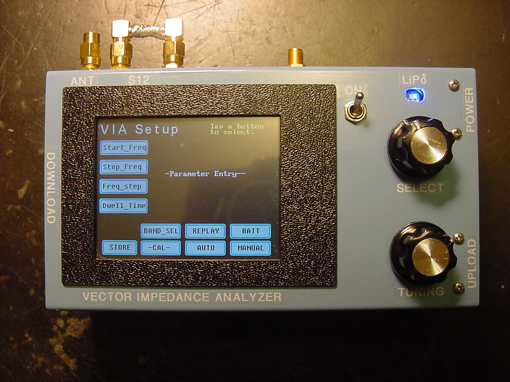
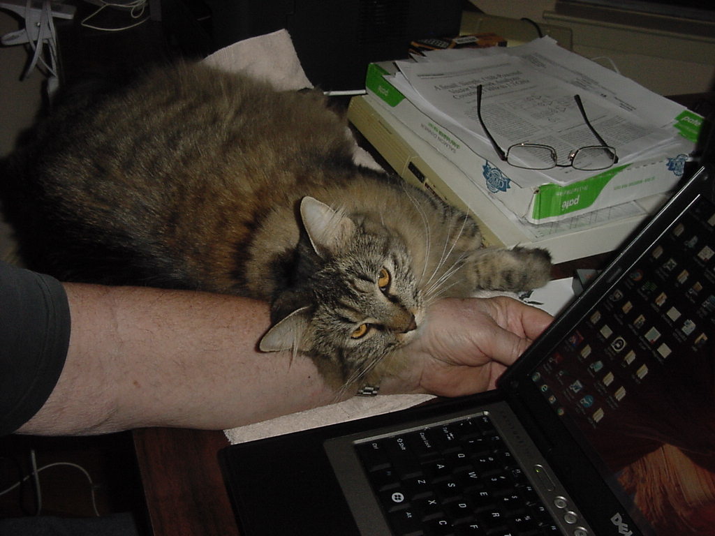
This is the K5BCQ VIA today. It is being used for S12 (filter insertion loss) testing. The VIA
has three Mini-USB connectors on the sides, one for downloading new firmware, one for uploading data
to your PC, and one for charging the LiPo batteries. All use the same 8" Mini-USB to USB cable. The
LiPo indicator shows "discharging" with a Blue LED and "charging" with a Red LED. That circuit comes
out of the LiPo battery pack. I didn't realize Sandy had used the last of the "Black on Clear"
Brother P-Touch tape. Can't blame the cat for that one.
The Manual BPF/LPF Switch Kit #26
THIS KIT IS PRESENTLY SOLD OUT .....ORDERING MORE PARTS, PLEASE CHECK BACK LATER
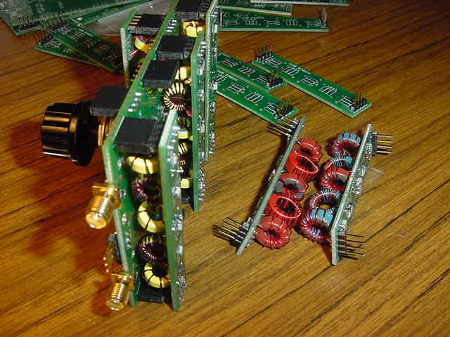
This is the 6 band, manually switched, Band Pass Filter and Low Pass Filter board.
It consists of a 2.5" x 3.5" host board with up to 6 individual 2.5" x 0.6" BPF filters or LPF
filters. It has multiple coax attach methods on the board: Coax cable directly with strain relief,
BNC connectors, or SMA connectors.....your choice. Signal traces on the board are 50 mils and
kept as short as possible with all wiring over a solid ground plane to minimize
transmission line problems on the board.
The 6 bands on the switch are plug-in and can be any 6 BPF or LPF filters. The assumption
being that for Tx you would probably want LPFs. However, if you want to use pluggable BPFs for
both Receive and Transmit, that's OK too. The board can be configured so that the onboard Tx/Rx
relay can be connected to either end of the symetrical plug-in filters.
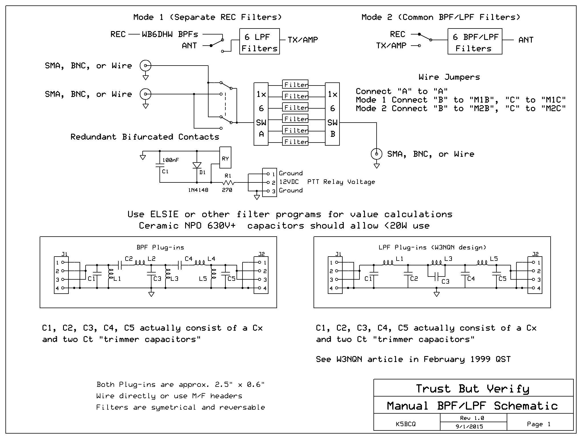
Manual BPF-LPF Switch Board V2.0 Schematic
In Mode 1 the relay armature switches the Antenna between the Receiver and Transmitter. The one
selectged plug-in filter is connected in series with the Transmitter output ONLY. This allows the
receiver to have it's own filters ......like Dave's, WB6DHW, broadband BPFs. In Mode 2 the 6
pluggable filters are connected to the Antenna at one end and the armature of the Tx/Rx relay
at the other end. The relay selects between Receive and Transmit and the filters are inline to
the antenna for both.
The relay is powered by 12V at 28mA and is controlled by external (Voltage active) PTT input.
It has gold, bifurcated and redundant contacts for reliability.
The little 2.5" x 0.6" BPF/LPF filter (shown in the Kit #15 section, above) form factor is not
a "standard" yet but they seem to fit in well with the size QRP SDR units around here (AQRP). I
measured a couple of LPFs for 40m and 20m on my MiniVNA-Pro and the Transmission Loss was <0.1dB
with a very respectable Return Loss so the SWR is low. Of course, all these maeasurements
are into 50 ohms. BPF data looks good too but I haven't built them up and tested them for all the
bands.
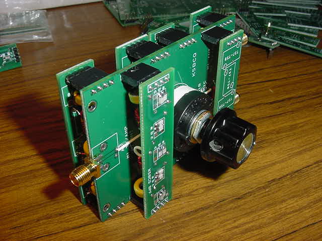
Some pictures showing more detail of the switch. The filters are symetrical and can be plugged
right side up or upside down. You can locate the header pins on either side of the board and can
come up with some very compact implementations. This compact technique works great for T37 cores.
For T44/T50 cores, use additional spacers where needed.
------------------------------------
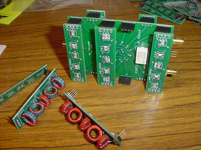
EXTERNAL FILTERS ......Individual Plug-in BPF and LPF filters.
THE FILTER BOARDS ARE IN PRODUCTION AND IN STOCK
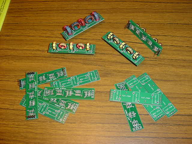
Shows several BPF and LPF boards
These boards all have a 2.5" x 0.6" form factor and come in two varieties, BPF or LPF. Redundant
header pins are located at both ends (or you can solder directly), The designs are symetrical so the
boards can be reversed or flipped without effect. The boards can be used standalone and plugged one
at a time or used with a switcheable host board of your design or mine (available later). I have
the bare boards only and header pins available for $2 per board plus postage in the USA. You would
use one of the free programs like Jim Tonne's, ELSIE, or other filter program (AADE, etc) for the
appropriate values for your needs.

