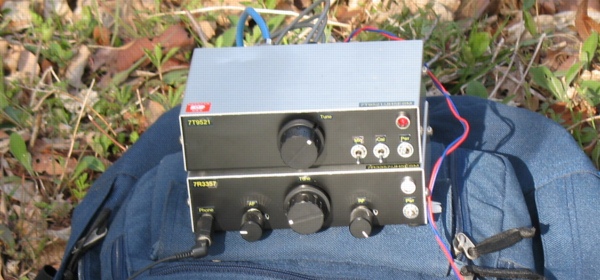
7T9521 “Komukai40” with 7R3357R “Fujimino40” at Iwajuku, Midori-city (JCC1612).
7T9521 “Komukai40” with 7R3357R “Fujimino40” at Iwajuku, Midori-city
(JCC1612).
Cosy MUTO, JH5ESM
15 April, 2006
Updated on 25 April, 2006
![]()
In 2005, I had built a transmitter featuring pre-mix VFO unit using ceramic resonator VXO. Since the VFO stability was not enough for field operation and collector efficiency at the final stage was so poor, I decided to build another configuration.
The new transmitter, 7T9521 (the
codename comes from "7MHz TX, 2SA950/2SC2120
for the final stage devices"), adopts varicap controlled VXO for
stability and features class-C SEPP, which has been successfully
experienced and implemented before, for high efficiency and low
harmonic distortion.
7T9521 now has a nickname "Komukai40."
The name comes from the place where Toshiba R&D Center locates.

The buffer output is followed by an LPF with 2nd harmonic trap.
Supply voltage for this section should be well stabilized.
I used a 5[V] low drop regulator with LED level shifter to obtain
8.8[V] supply voltage.
It covers 7.001 to 7.009[MHz] and the 8[dBm] output is achieved.
The driver stage is a class AB
tuned amplifier. The idle and operation currents are 11[mA] and 22[mA],
respectively.
Since the output impedance is estimated to 220[Ω] and the resonator QL
becomes approximately 4.5, the driver resonator made of fixed value
capacitor and inductor is sufficient for resonance frequency tolerance.
The keying is made at collector supply of this stage. To suppress key clicks, time constant elements (33[Ω] and 33[μF]) are inserted at supply line.
The output swing is 13[Vpp] for 220[Ω] load at 13.5[V] supply and it is enough to drive the SEPP power stage.
Push-pull configuration is a good choice for power amplifier because its even order harmonics are smaller than the single amplifier case. The successful class C SEPP configuration (the design procedure is here) is employed again.
2SA950 and 2SC2120 are complementary pair made for 1[W] class audio amplifier, but also can be used in lower HF band. You can find similar devices for alternatives. For example, BD135 and BD136 are candidates for 2[W] or more: but it is not tested at my site :p
Harmonics are rejected by the 5th order
LPF with transmission zero at 14[MHz].
A relay controlled semi break-in and
the supply keying is employed.
The relay switches antenna connection and VFO supply line. Break-in
delay can be adjusted. For full QSK application, the relay should be
replaced by electronic switches.
For transceive operation, some control connection with the receiver should be implemented. In this design, RX antenna, power supply, remote and the keying signals are provided for this purpose.
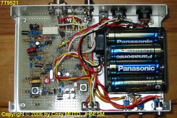
The whole circuit shown in
Fig.1 is implemented onto a 95×72[mm] universal breadboard
and the whole transmitter including 8(eight) AA batteries are
put into 150×40×100[mm] enclosure, as shown in Fig.2.
Note that the enclosure comes from 7T2120pp, and its breadboard is
replaced by 7T9521.
 |
 |
 |
| (a) Overview | (b) Top view | (c) Breadboard |
Preliminary test results for the driver
circuit is shown in Fig.3.
As seen from the input-output response, the circuit does not act as a
linear amplifier.
Class A biasing is required for linearity.
The frequency response shows that fixed
value components for resonator works well for this application.
Note that the driver also responses to 3.5[MHz] input signal. The
circuit also acts as a frequnecy doubler.
Output swing response to the supply
voltage shows very good linearity. It means that the circuit can be
used for QRP AM modulation.
 |
 |
 |
 |
| (a) Experimental driver. | (b) Input-output response. | (c) Frequency response. | (d) Supply voltage response. |
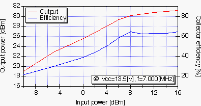
The experimental board and its performances are shown in Fig.4.
The input-output response shows that
the circuit has 1[W] output capability for 8[dBm] input signal and
60[%] efficiency can be expected.
It also works on 9[V] supply, but it goes to QRPp mode :p.
 |
 |
 |
| (a) Experimental board. | (b) Input-output response | (c) Supply voltage response. |
Frequency stability is tested under open-air, room temperature condition. As seen from Fig.5, it is very sufficient for operation.

Fig.5 VXO stability from cold
start.
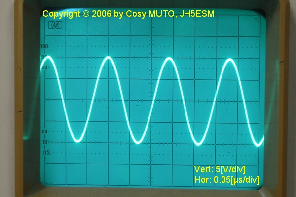
The
output waveform is shown in Fig.6. It is easy understand that
1[W] output is achieved without visible harmonics. Although the PA
transistors are standard TO-92 package and no additional radiator is
provided, it works well. In addition, QRPp transmission can be expected
even if the supply voltage drops to 9[V].
 |
 |
 |
| (a) Waveform at 50[Ω] load. | (b) Continuous operation. | (c) Supply voltage response. |
![]()
![]()