Solid State Circuits 5 -
1. Single Emitter Follower
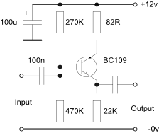
2. Dual Emitter Follower
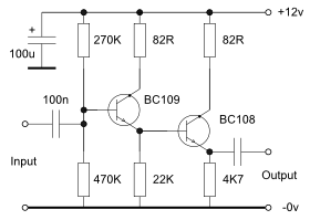
3. Bootstrapped Emitter Follower
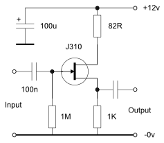
4. Source Follower
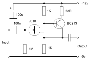
5. Source Follower and Bipolar Amplifier
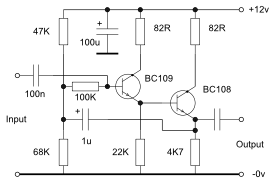
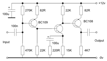
6. Buffered LF Amplifier
|
Circuit 1 has a lower output current capability than circuit 2. |
|
|
|
|
|
These figures apply to circuits 1 & 2 |
|
|
Input Level pk- |
Output Distortion |
|
1v |
<0.1% |
|
2v |
<0.1% |
|
3v |
0.10% |
|
4v |
0.13% |
|
|
|
|
Voltage gain |
Just under 1 |
|
Frequency response |
Flat to at least 1MHz |
|
Input impedance |
170K |
|
|
|
|
Note: Emitter and Source Followers can oscillate with inductive input loads like screened cables. If this occurs place a 100R resistor in series with the input close to the device. |
|
|
This circuit uses a bootstrap feedback to increase the input impedance with a minor increase in output distortion at higher input levels. |
|
|
|
|
|
Input Level pk- |
Output Distortion |
|
1v |
<0.1% |
|
4v |
0.19% |
|
|
|
|
Voltage gain |
Just under 1 |
|
Frequency response |
Flat to at least 1MHz |
|
Input impedance |
5M6 |
|
This circuit uses a Junction FET to provide a very high input impedance determined by the gate resistor. |
|
|
|
|
|
Input Level pk- |
Output Distortion |
|
1v |
0.52% |
|
2v |
1.15% |
|
3v |
2.25% |
|
|
|
|
Voltage gain |
Just under 1 |
|
Frequency response |
Flat to at least 1MHz |
|
Input impedance |
1M0 |
|
|
|
|
The distortion should improve with a higher supply voltage subject to the device specification. |
|
|
This circuit uses a Junction FET followed by a pnp amplifier and negative feedback to reduce the low level distortion in circuit 4. |
|
|
|
|
|
Input Level pk- |
Output Distortion |
|
1v |
0.12% |
|
2v |
0.25% |
|
3v |
2.07% |
|
|
|
|
Voltage gain |
1 |
|
Frequency response |
Flat to at least 1MHz |
|
Input impedance |
1M0 |
|
|
|
|
Increasing the supply to 24V reduced the distortion at 2v ouptut to 0,12%. |
|
|
- |
17Hz - |
|
Gain |
x90 |
|
|
|
|
Output level pk- |
Distortion |
|
2v |
3.2% with 12v supply |
|
4v |
1.4% with 24v supply |
|
|
|
|
Input impedance |
170K |
7. Single Stage LF Amplifier
|
Emitter Potentiometer Setting |
Voltage Gain |
Input Impedance (ohms) |
|
Minimum |
x5 |
7K |
|
Halfway |
x8.8 |
6K9 |
|
Maximum |
x258 |
4K7 |
The minimum setting is with the slider at the 0v end.
As the collector has an almost constant current characteristic the output impedance is effectively the value of the collector resistor i.e. 4K7ohms.
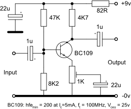
Simple single stage amplifier measured at three settings of the emitter potentiometer. Capacitor values are for voice communications applications so will need to be increased for HiFi uses. Onset of clipping at output level = 7v pk-
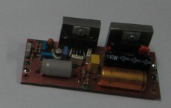
8. Example Audio Amplifier and 9V Regulated Supply
The adjacent photo shows a completed audio amplifier using a TDA2003 and a simple 9V supply using a 9V LDO regulator, both running from an external 13.5v DC supply.
The aluminium blocks are bolted to the PC board and provide a support for the two integrated circuits during test and one mounting facility for the module in the completed equipment. In addition the PC board has 8BA clearance hole for 8BA tapped mounting spacers.
The PC board is 83mm x 37mm and the aluminium blocks are 23mm high.