Solid State Circuits 2 -
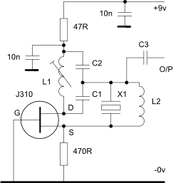
Crystal Oscillator 1
This circuit can be used from low frequencies to at least 120MHz using series resonant crystals on their fundamental or overtone mode. The output can be taken from the feedback tap as shown, a low impedance winding on L2 or from the drain of the J310 via a low value capacitor. The following stage should be used a a buffer to isolate subsequent stages from the oscillator.
The combined series value of C1 and C2 resonates with inductor L1 at the desired frequency and crystal X1 must have a fundamental or overtone series resonance as appropriate at the same frequency. C2 is about five times the value of C1
Inductor L2 is generally only required at frequencies above about 60MHz and must be chosen to resonate with the total parallel capacitance of X1 at the frequency of oscillation. If the circuit shows signs of free running oscillation controlled by L1 then L2 will be required. The parallel capacitance of X1 will typically be 4 -
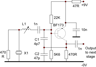
Crystal Oscillator 2
This circuit is primarily intended for use as an overtone oscillator and will work from 20MHz to 120Mhz depending on the crystal and active device. Operation is extremely stable but the output level is fairly low -
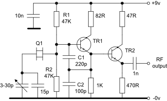
Crystal Oscillator 3
This circuit is a Colpitts fundamental mode parallel resonant oscillator for crystals designed for use with a 30pF load capacitance. Values shown are suitable for 8 -
If problems occur getting oscillation to start between 1-
This circuit has been shown to be problematic below 1MHz because of higher crystal losses.
|
Frequency |
C1 |
C2 |
|
1- |
680p |
470p |
|
3- |
470p |
220p |
|
5- |
220p |
100p |
|
10- |
150p |
68p |
The 470R resistor across the crystal suppresses oscillation at the parallel resonant frequency and must not be omitted. Most RF characterised transistors will work in this circuit. An alternative output may be taken from the collector by inserting a low value 82R -
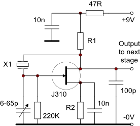
Crystal Oscillator 4
This fundamental mode Pierce oscillator can be used over a wide frequency range with little or no changes to component values. The circuit to the right was originally developed by myself in the 1970s using a 2N5245 RF JFET which had a relatively low Idss range but they are now very difficult to obtain. A J310 has been used instead which has an Idss range of 24 -
The table below shows the results for a single test device selected at random from new stock.
|
|
R1 = 6K8, R2 = 4K7 |
R1 = 2K2, R2 = 1K5 |
R1 = 680R, R2 = 470R |
|
Crystal Frequency |
Drain voltage pk- |
Drain voltage pk- |
Drain Voltage pk- |
|
85KHz |
4.2v |
No oscillation |
No oscillation |
|
450KHz |
3.9v |
4.1v |
4.2v but slow to start |
|
1MHz |
4.4v |
4.1v |
4.6v |
|
2MHz |
4v |
4.2v |
4.2v |
|
3.395MHz |
3.3v |
4.9v |
6.1v |
|
12.395MHz |
1.2v |
2v |
3.9v |
|
20.0MHz |
400mV |
800mV |
1.1v |
Although the higher value drain resistor gives more gain at the low frequencies, there is an obvious reduction in output level at the higher frequency end due to the RC time constant impacting on circuit gain and slew rate.
As with most oscillators the output power level is low. If it needs to be distributed around a number of circuits then an emitter follower or equivalent buffer stage should be included. A bipolar npn emitter follower may be DC coupled to the FET drain via a 47ohm resistor to suppress any tendency to oscillate at VHF.
If you decide to replace the drain resistor with an RF choke then the emitter follower should not be DC coupled to the drain as the drain voltage will exceed the supply line on positive half cycles.