PC Board Layout -
Graph Paper Method
Having completed your electronic design prototype, the next step is to make a PC board to hold and connect the various parts. Easy? Difficult? Well that depends on how you go about it. The first and most important step is to draw the circuit diagram of your module following good 'RF' rules i.e. keep the input and output apart, go in straight lines not circles, keep connections short and use the maximum possible ground copper. In other words, think about the layout of the circuit diagram and if necessary draw it again until you are happy with it. Minimise cross-
RF design rules require inputs and outputs to be kept apart, connections and decouplings to be as short as is possible, ultimately dependant on the frequency of operation, the gain and shielding requirements. If necessary, use a double sided PCB with the component side dedicated as a ground plane with the copper only cleared away from component leads that are not connected to the ground plane -
If you have a CAD package on your computer that you are happy with then use that. Otherwise:
I start with a piece of 0.1 inch squared graph paper, 2H or 3H pencil (0.5mm diameter lead), soft eraser and a final copy of the circuit diagram. The intention is to make the PC layout follow the circuit diagram layout and most electronic components will fit imperial graph paper more easily than metric paper. With the exception of really high density boards, I have always found this relationship holds between circuit and PC layout and with surface mount components easily available most things are possible.
I draw the layout looking at the solder side of the PCB although a lot of PC CAD packages view the board from the component side. If you are going to hand paint the board then you need a view from the side you will paint. Some CAD packages will allow you to edit and print the copper patterns as viewed from either side.
Start by making a separate layout drawing of each component that you are going to use and decide on the lead spacing of components like resistors, capacitors etc where the spacing is open to choice -
Then sketch the approximate layout on a piece of scrap paper, allocating groups of components like an oscillator or amplifier to a space on the layout. Decide roughly where you wants connecting pins on the edge of the board. Now place the components for each stage onto a layout in the same order and layout as the circuit. At this stage, the layout will probably look a bit disorganised and too large -
With difficult layouts you can use the top copper to implement cross-
Practice makes perfect so the second time you do a PCB it will be better and take less time. Start with a simple board to ease your learning phase. The centres of pads should be marked with a small but clear black dot so that they may be seen easily when using a photocopy of the layout to drill the board.
Example lead spacing rules for wire ended miniature components:
- 0.25W resistors -
0.3” (7.5mm) - 0.33w resistors -
0.4" (10mm) - 0.5W resistors -
0.6” (15mm) - Disc ceramic capacitors -
0.1" (2.5mm) or 0.2" (5mm) depending on each type of component - TO18 / TO72 semiconductors -
0.15" (3.8mm) per side (triangle or square) - 1N4148 and similar diodes -
0.4" (10mm) - 1N4000 series diodes -
0.6" (15mm) - 1N5400 series diodes -
0.8” (20mm)
You can put component pads as close as 0.1" between lead centres but they are more difficult to hand paint -
When you are happy with the finished layout see the article on making your own boards here.
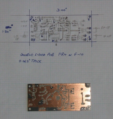
An example of my graph paper process is shown below together with a part painted board. I use a darker paint colour for ground copper and a lighter paint colour for non-