PC Board Construction -
Image Transfer Method
The following notes have been provided by my friend Chris Potter as I do not use this method. Please note that the chemicals used in this process are extremely dangerous.
If in doubt get some assistance from an experienced person.
1) Draw a schematic and design a layout using pcb program
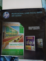
2) Print out on laser paper on a laser printer -
3) Clean copper board using a worn foam rubber sanding block, clean with acetone
4) Tape printed image to board , printed side to copper
5) You now have 2 options
a) Use a very hot clothes iron for at least 90 seconds to 2 minutes
or
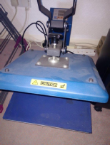
b) Use a shirt press , set temp to 200C and time for 90 seconds, lay copper side up and place some A4 paper on top to stop sticking as the heating element is on top
6) Let it cool, as it will be very hot and easily burn you
7) Place board in water and gently rub until paper falls off, don’t rush this part otherwise the layout will be damaged -
8) Etching part, this must be done in a well ventilated area as using very strong chemicals , I use a extractor fan
9) I use 35% hydrochloric acid only 1 cap full, use at arms length and do not breath in the fumes which are very toxic / potent
10) Add 2 capfulls of 6% hydrogen peroxide
11) Use a plastic container, something like a ice cream tub
12) Drop in pcb and keep the liquid moving, do not let it sit otherwise undercutting may result
13) It will etch very quickly (more peroxide equals more time)
14) When etched drop into a jar of water and wash and dry
15) Use acetone for final clean on new board and if all goes well you should have a perfect board ready for soldering
16) a word of warning, be very careful with 35% acid and keep a bucket of cold water nearby just in case of splashes on skin. Always wear safety glasses.