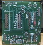
Digital Interface PCB v.II.2

Digital Interface PCB v.II.2
OVERVIEW
The story begins when on February 2001 Elecraft awarded me the honor of publishing my article on how to modify the K2 to bring out signals for digital modes, entitled "K2's Mic Configuration Header Extender and Rear Panel DATA Connector", as the Elecraft's February 2001 Featured Article. Thanks Elecraft.
(This article is available as a pdf file at my downloads page, on the K2 DIGITAL INTERFACE v.II.2 link.)
The need of a way to modify the K2 to bring out signals for digital modes with a fixed and independent audio level was the leitmotif of that article and it is still valid but not so much so the how I did it. The original method became stale dated. I might add that my first approach at the design of a circuit to develop the project was quite a success as my small stock of prototype PCB's (15 units) was very quickly allotted.
All was ok (or so I thought) until I received some feedback asking me if I could consider the possibility of modifying my circuit in such a way that the front panel mike's AF and PTT lines be cut when transmitting digital data through the rear connector, so as to avoid any chance of a live mike transmitting unwanted sound (shack's noise) along with the digital signal.
I gave a thought to those suggestions and came to the conclusion that, so long as I had extended the K2 mike's configuration header from the Front Panel board to my K2 Digital Interface for an easy access, the mod suggested was easy to make and at the same time I could improve the circuit that amplifies the received audio coming from J5 at the K2 RF Board.
K2 DIGITAL INTERFACE II.2
The following table of text and images is the result of my efforts to reach that goal: The K2 Digital Interface II.2 that features a Mike Configuration Header Extender and Rear Panel Data Connector, as well as a buffered, fixed audio output and the cutting of Front Panel mike connector's AF and PTT lines, when transmitting data.
Clicking on any and all of the thumbnails a new window will be opened to display an enlarged picture of the chosen snapshot. To close that new window just click on the image displayed.
COMMENTS
This printed circuit board was designed on July 2001, when I had it installed and working in my K2. At the same time, Jay Rutherford, K1UC, did the field testing of the project for me, with good results I might say. Hi Jay, thank you for your invaluable help!
At that time Elecraft had not yet released the KAF2 option an thus there was some room available within the K2 to install the D.I. as I did, but the time came when Elecraft made the KAF2 available and, as I have all the options installed, I ordered it. I constructed the option and I installed it. The KAF2 works fine business but ... Oh dear! ... I had to uninstall my Digital Interface as it collided with the new option. The KAF2 needed the space my PCB was occupying. ~:-(
Latter on, the KDSP2 option, an extraordinary filtering device, was launched and occupied the place of the KAF2.
My premonitions had come true; the K2 was so stuffed with all its options and cables that there was no room left for an alien modification. That is the reason why I withheld the info about my project.
To cut a long story short, up to that moment my July 2001 project seemed to be valid only for those K2rs that had not installed and did not intend to install either the KAF2 or the KDSP2 option and/or the KBT2 Internal Battery option.
It also appeared that those K2rs that went QRO by constructing the KPA100 and had it installed on top of the basic K2, in lieu of the top cover containing the KAT2, KBT2 and/or KIO2 options, to conform the K2/100 set-up, had no choice and could not install my Digital Interface.
NEW IDEAS, NEW SET-UPS
Now I am glad to say that currently this situation is no longer true. Some day, by mid November 2003, I was struck by some new ideas:
I managed to find what I thought was the right place where to install my DI v.II.2 within the integrated K2/100. The only change needed is the use of low profile parts (connectors and capacitors).
After that, I designed a new and smaller PCB for my DI: The K2DI v.III, same circuit with different placement of parts, suitable for the QRP K2 set-up (with either the KAF2 or KDSP2 as well as the KBT2 options installed) and/or the split QRO K2/100 set-up, with the KPA100 and KAT100 remotelly installed in a separate EC2 enclosure.
And I also designed an optional daughterboard for the K2DI vIII Digital Interface, the K2DI-PCI Computer Interface, featuring selectable Serial (RS232) or Tone PTT and direct connectivity to the computer's sound card with Line In and Line Out isolation through a couple of 600:600 transformers. The Serial PTT is also isolated by an optocoupler.
Modified on February 17, 2004.