PIC Notes by DL4YHF
Original file location: ?/datasheets/pic/DL4YHF_PIC_Notes.htm
Link to the website: www.qsl.net/dl4yhf/pic/DL4YHF_PIC_Notes.htm
/ back to the index.
Finding the right PIC (or similar microcontroller) can be daunting,
especially on the Microchip website with sooo many broken links.
This file started as list of notes by the author (DL4YHF), written when searching
for the 'smallest' dsPIC33 in homebrew-friendly through-hole PDIP with "High-Speed PWM").
Later, this document turned into a chaotically organized kind of 'notebook'
with (ds)PIC-related info collected from various projects in the 2020s.
The days of programming 8-bit PIC in assembler are mostly over, since
fairly modern dsPICs are still available in homebrew-friendly plastic
standard DIP. What used to be the PIC16F84 decades go ("homebrew friendly"
microcontroller without too many whistles and bells) may now
be a dsPIC33EP512MC502-I/SP or similar, with plenty of Flash (512 kByte),
fairly large RAM (48 kByte). If only there wasn't this incredibly sluggish,
mimosa-like 'development system' (MPLAB-X), where -in older versions- a single step
in the debugger took at least half a second... and terminating a debug session
sometimes took minutes.
In the 2020s, using a multi-core PC with several Gigabytes of RAM for development,
MPLAB-X became more usable (in combination with a PICkit4), so for simple projects
which don't require the CPU power of an ARM Cortex-M, even the old PIC16 devices
are still a good choice - e.g. in some battery-powered projects where the DC supply
current for a PIC is measured in microamperes, not milliamperes
- see notes about low power design
in a later chapter.
- Special features in certain PIC families
- dsPIC33 'High Speed PWM' vs. other 'Fast PWMs', 'High-Res PWMs', etc
- dsPIC33 'High Speed PWM' interconnected with 'High Speed Analog Comparator'
- dsPIC33 'High Speed PWM' synchronizing the 'High Speed ADC'
- Properly clocking the High-Speed-PWM (for 1.04 ns resolution)
- Four 'bonus PWM's in dsPIC33EP32GS502 : "Output Compare with dedicated timer"
- Where are all those pins (PWM, comparator, etc) in a dsPIC33EP32GS502 (SOIC-28) ?
- The dsPIC33E's clock system
- The dsPIC33E's Oscillators
- The dsPIC33E's 'FRC Oscillator'
- The dsPIC33E's 'Primary Oscillator' (Crystal Oscillator)
- The dsPIC33E's 'Main PLL' (feeding the 'core')
- The dsPIC33E's 'Auxiliary Clock Generator' (feeding the PWM)
- dsPIC33EP32GS502 current consuption (measured) with different clock setups
- The dsPIC33E's Serial Peripheral Interface
- The dsPIC33E's different (and incompatible) ADC flavours
- dsPIC33E (newer) versus dsPIC33F (older)
- Low-power design with PIC16 / PIC18
- Notes about developing with MLPAB-X and XC16
- The hassle with MPLAB-X include file paths for the C compiler
- Predefined symbols for the C compiler (stored in the MPLAB-X project ?)
- MPLAB "Code Configurator" ? (give it a try - but only for the initialisation)
- dsPIC33EPxxGSxxx High-Speed PWM setup via MCC ?
- XC16 Interrupt Vectors (and how to find the names for interrupt handlers in "C")
- XC16 "Fuse Bit" names and values (or: how to find the names for #pragma config in "C")
- XC16 Built-in Functions (or: no "nop()" anymore..)
- Efficient storage of tables in code memory
- Simple (but wasteful) tables in Program Memory Space
- Packed (but slow) tables in Program Memory
- Debugging with MPLAB X and PICkit 3/4
- How to program a "standalone" firmware with PICkit 3/4
- PICkit 3 : The never-ending hassle with 'Failed to program device'
- More 'fun' with MPLAB X : "The target device is not ready for debugging"
- Even more 'fun' with MPLAB X : "No Tool" ... despite a healthy PICkit 3 or 4 connected to USB
- MPLAB-X, PICkit 4, and a dsPIC33EP : Sluggish response during a debug session
- MPLAB X : Project suddenly fails to load due to missing header files
- MLPAB-X Debugger flaw: "Halting... Time out waiting for tool lock"
- Migration from MPLAB X Version 5.50 to Version 6.20 (2024-03)
- Fairly new PIC projects by DL4YHF
- Improvised 'eval board' for dsPIC33EP32GS502
- Locally saved PIC datasheets and appnotes
1. Special features in certain PIC families
1.1 dsPIC33EPxxGSxxx 'High Speed PWM' versus other 'fast' PWMs
From dsPIC33E High Speed PWM DS70645C :
- Up to seven PWM generators, each with an individual time base
- Two PWM outputs per PWM generator
- Individual period and duty cycle for each PWM output
- unlike other "Fast PWM" modules, THIS ONE doesn't mention the maximum resolution.
Unfortunately there's no list of devices supporting exacly this flavour
of 'Fast PWM'.
From dsPIC33 High Speed PWM DS70000323H :
- Up to nine PWM generators (the big question was WHERE ?)
- Two PWM outputs per PWM generator
- Individual time base and duty cycle for each PWM output
- Duty cycle, dead time, phase shift and a frequency resolution of 1.04 ns
Unfortunately there's also no list of devices supporting exacly this flavour
of 'High-Speed PWM'. You need to know the device to check if a particular
'Family Reference' / High-Speed/High-Res/Whatever-PWM applies. So far, references to
"DS70000323" or sometimes "DS70323" could only be found in:
- The dsPIC33EPXXGS202 FAMILY, but only TREE PWM generators of this "fast" type;
insufficient for a planned RGBW-LED PWM controlled current source / colour mixer
- The dsPIC33FJ64GS.. family was said to have the "1.04 ns PWM resolution",
but not available in homebrew-friendly SOIC or even PDIP (the entire family
is TQFP-64 or larger .. yucc).
- dsPIC33FJ06GS001/101A/102A/202A also has "1.04 ns PWM resolution",
is available in SOIC or even PDIP but only has THREE 'High-Speed PWM pairs'.
Despite not being a "MC" (MotorControl) but a "GS" ("DigitalPower"??) chip, a single PWM cycle
can be stopped via "High-Speed Comparator with direct connection to the PWM module".
Very nice for any kind of switching-mode converter with switch current limiter.
Why don't the "MotorControl" devices have this ?
- dsPIC33EP16/32/64GS502: Has FIVE
of these "1.04 ns resolution" PWMs, is avaliable in SOIC-28 (but not in SPDIP anymore),
"dsPIC33EP32GS502-I/SO" available "On Stock" at Mouser (3.2 Euro),
and Digikey in 03/2021.
Beware : Like many "newer" dsPIC33s, NO EEPROM (but Flash is "run-time self-programmable" and eraseable
in 1536-byte-blocks at a time) !
- dsPIC33FJ16GS502-50I/SP: Has FOUR
of these "1.04 ns resolution" PWMs, two 4-MSPS 10-bit ADCs, is avaliable in SPDIP-28,
"dsPIC33FJ16GS502-50I/SP" was available "On Stock" at Mouser for 4.3 Euros in 03/2021.
Beware : Like many "newer" dsPIC33s, NO EEPROM (but Flash is "run-time self-programmable" and eraseable
in 1536-byte-blocks at a time) !
- dsPIC33FJ32GP202/204 doesn't have the "1.04 PWM resolution",
but is availabe in PDIP-28. Only has "three timers" and "two Output Compare" units - bleah..).
Neither a "DigitalPower" (GS) nor "MC" (MotorControl) but a "GP" (GeneralPurpose?) device,
doesn't have much to offer for any kind of switching-mode or PWM output.
- dsPIC33FJ32MC202 with "MC" = "MotorControl:
Is availabe in PDIP-28, also has a "High-Speed PWM" with "up to four PWM pairs with
independent timing", but only 12.5 ns PWM resolution (still ok for low-frequency SMPSU)
From DS70005320 "High-Resolution PWM with Fine Edge Placement" :
Even though this document also is part of the "dsPIC33/PIC24 FRM" (Family Reference Manual),
it quite likely only applies to dsPIC33C (which, contrary to the letter sequence, is much
younger than e.g. dsPIC33F, and a bit younger than dsPIC33E). As usual, this document itself
doesn't contain a list of devices to which it applies.
This "FRM" claims a PWM resolution of 250 picoseconds in "high-resolution"
mode but as usual, there's a price to pay for this (it doesn't work in this mode,
it doesn't work in that mode, it only works if you use a certain oscillator
to feed the PWM, etc). Also, ..
> High-Resolution mode is not available on all devices.
> Refer to the device-specific data sheet foravailability.
Unlike the older "high-SPEED PWM" from e.g. dsPIC33EPxxGS502,
this "high-RESOLUTION" only seems to apply to the PWM "phase, duty cycle, and dead-time
resolution" but it doesn't mention the PWM period (which quite likely will
still be limited to the input clock for the PWM divided by some integer.
All formulas seen so far for the PWM frequeny (or the inverse, period)
had 'F_PGx_clk' in the numerator and and integer expression in the denominator,
thus it's unlikely to use this "HR-PWM" as the heart of a programmable RF generator
with fine frequency steps.
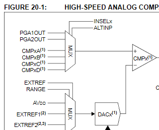
1.1.1 dsPIC33 'High Speed PWM' interconnected with 'High Speed Analog Comparator'
Some devices with the 'High-Speed PWM' also have a few 'High-Speed Analog
Comparators' that can be tied to the PWM for...
- PWMx duty cycle control (great for SMPSU switch-current limiting during the 'inductor charging' phase)
- PWMx period control
- PWMx Fault detected
The above High-Speed comparators, connectable to the High-Speed PWM,
were seen in datasheets for ...
- dsPIC33EP16/32/64GS502 (5 HS-PWMs, 4 HS comparators, even for the SOIC-28 devices),
- dsPIC33FJ16GS502 (4 HS-PWMs, 4 HS comparators, beware: ..GS402 has NONE),
- ... ?
Details are not in the PIC datasheet but (for the dsPIC33 'GS' devices listed above)
in DS70000323, chapter 17,
"PWM interconnects with other peripherals", e.g.:
The truncation of the PWM pulse is accomplished with no software intervention,
and can be programmed to respond to a variable threshold.
The analog comparator can also be programmed for inverted polarity selection.
For example, the inverted polarity may be useful in detecting
an undervoltage condition or the absence of a system load.
Chapter 10.1 "PWM Fault Generated by the Analog Comparator" shows an example
for the dsPIC33FJ(16/06)GSxxx, which configures the analog comparator as a
'Fault Source' to the PWM (requires unlocking certain registers, before
configuring some 'Virtual Pins' like RP32 to connect the comparator output to RP32,
and RP32 as 'Fault Input' to the PWM.
Details about the dsPIC33FJ(16/06)GSxxx'es High-Speed Analog comparator are in
DS70296 (not in the datasheet).
Quoted from there:
The High-Speed Analog Comparator module in Switch Mode Power Supply (SMPS)
and Digital Power Conversion devices provides a way to monitor voltage
and current in a power conversion application. The analog comparator
provides the user with the ability to implement Current Mode Control (CMC)
in power conversion applications. The High-Speed Analog Comparator module
contains up to four high-speed analog comparators with dedicated 10-bit
Digital-to-Analog Converters (DACs), which provide a programmable reference
voltage to one input of the comparator.
Whow ! That would reduce the external circuitry for the planned RGBW-LED
switching-mode colour-mixing constant current supply (for OSRAM OSTAR
LE RTDUW S2WP). At a maximum of 5 Ampere switch current, the current
sense resistor would be 40 mOhm or less (40 mOhm would dissipate 1 Watt
at 5 A), so how would the comparator(s) in a
dsPIC33FJ16GS502
cope with that ? From DS70296C page 45-11:
The High-Speed Analog Comparator has a limitation for the input
Common Mode Range (CMR) to not exceed(AVDD - 1.5V).
The HGAIN bit (CMPCONx <2>) is enabled, and
the High-Speed Analog Comparator input Common Mode Range (CMR)
can be extended to 3V. This means that both inputs to the comparator
(the selected CMPx input pin and the selected reference source)
should be within this range. As long as one of the inputs is within
the CMR, the comparator output will be correct.
However, any input exceeding the CMR limitation will cause
the comparator input to be saturated. If both inputs exceed the CMR,
the comparator output will be indeterminate.
-> To monitor / limit the current through the high-side switch in a
buck converter (R_sense between the SOURCE of a P-channel MOSFET
and the positive supply rail), we need to 'level-shift' the voltage
across R_sense towards the PIC's analog ground anyway, and on
that occasion, we can also 'amplify' the few millivolts for the PIC's
analog comparator input.
BUT: The "same" functional block (analog comparator) in a
newer dsPIC33EP32GS502
had a higher common-mode voltage, and lower offset error
- see dsPIC33E versus dsPIC33F.
For this dsPIC, forget DS70296 and read DS70005128 instead:
The High-Speed Analog Comparator has a limitation for the input
Common-Mode Range (CMR)to not exceed (AVDD + 0.2V).
This means that both inputs to the comparator
(the selected CMPxinput pin and the selected reference source)
should be within this range. (...)
Note the subtle but important difference: Max. comparator
input voltage not 1.5 V below the analog supply voltage,
but 0.2 V above the analog supply voltage for a dsPIC33EP32GS502.
This is what others would call "rail-to-rail capable",
since for this particular family, the analog supply
voltage, and the DAC reference voltage,
may be as high as the digital supply voltage (3.6 V).
Clamp the input to Vdd with a Schottky diode (Uf < 200 mV),
and the comparator's output stays 'correct'.
1.1.2 dsPIC33 'High Speed PWM' synchronizing the 'High Speed ADC'
In a project using a dsPIC33EP32GS502
as a switching-mode constant current source, the HS-PWM used one of the high-speed comparator
to truncate the PWM cycle when the inductor current rose above a certain limit. The comparator itself
was feed by one of the programmable gain amplifiers, because the voltage drop
across the current-sense resistor was too low (only a few hundred mV) to drive
the ADC and comparator directly. To check the offset voltage (error) from the PGA,
and to check the inductor current waveform, both (ADC and comparator)
were connected to the internal output of PGA1.
To measure the inductor current shortly before the 'upper' MOSFET,
the ADC must be synchronized by the HS-PWM. How to achieve this ?
- DS70005127D shows on page 230, in the "ADC MODULE BLOCK DIAGRAM":
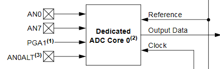
Only "Dedicated ADC Core 0" has one of its inputs on "PGA1".
Hmm. Is "PGA1" (the name they use for one of the ADC's inputs)
the same as "PGA1OUT" (the name they use for the input
of the High-Speed comparator, DS70005127D page 230) ?
- DS70005213G
doesn't specify which ADC core can be tapped to which 'analog source'.
It only mentions "From Other Analog Modules" (e.g. on page 4).
The description of "ADCON4H" on page 18 says:
> Refer to the device data sheet for the available ADC cores
> and their input channel options.
A-ha. For the dsPIC33EP32GS502, this takes us back to DS70005127D.
- DS70005127D page 239, about "ADCON4H" bits 1..0 = "C0SHS"
= "Dedicated ADC Core 0 Input Channel Selection bits":
0b10 = "PGA1" .
Ok, modified this as described in
file:///C:/pic/dsPIC33EP32GS502_RGBW_LED_SMPSU/dsPIC33EP32GS502_Drivers/adc.c.
On that occasion, also changed the clock source for the HS-ADC from the
wobbly "FRC" to the crystal-driven "APLL" (aka "Auxiliary PLL",
which in this case also fed the HS-PWM).
- Maxium allowed, and minimum required "ADC clock" for the maximum sampling rate ?
The datasheet
(here: DS70005127D page 345)
tells us the minimum ADC clock period is 14.28 ns, thus the
maximum ADC clock frequency seems to be 70 MHz.
The Family Reference
(here: DS70005213G page 43)
tells us Mr. HS-ADC has a conversion time of
8 * Tcoresrc + (bit resolution + 2.5) * Tadcore,
where "Tcoresrc" is the INPUT CLOCK into the "input clock divider",
and "Tadcore" is OUTPUT CLOCK from the "input clock divider".
For the "Dedicate ADC Core 0", that divider is controlled
by ADCORE0H.ADCS (a 7-bit group):
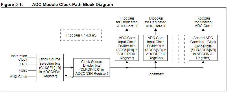
Example with "AUX Clock" = FAPLL = 16 * 7.3728 MHz = 117.9648 MHz:
FCORESRC = 117.9648 MHz / 2 = 58.9824 MHz, TCORESRC = ca. 16.9 ns (ok),
FADCORE = FCORESRC / 1 = 58.9824 MHz, TADCORE = FCORESRC = also 16.9 ns,
FSAMPLE = FCORESRC / ( 8 + 12[bits] + 2.5 ) = 2.62144 MSamples/second.
That's a sampling interval of ~~400 Nanoseconds, not sufficient to detect
cross-conduction (current spikes) by letting the ADC run at full throttle.
Instead, to detect cross-conduction and "automatically" optimize the HS-PWM's
dead-time register settings, the ADC conversion must be carefully synchronized
by the HS-PWM module as explained further below by shifting the sampling point
("trigger" from the ADC's point of view) by a 8 nanoseconds over subsequent PWM cycles
(unfortunately not the full HS-PWM resolution, 1.04 ns).
- DS70000323H explains "PWM-ADC Interconnect":
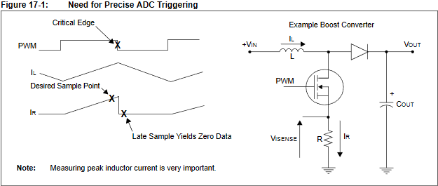
From DS70000323H ('High-Speed PWM Module' for dsPIC33EPxxGS):
"Measuring peak inductor current is very important."
The scenario previously described
can be prevented by using the flexible ADC triggering features of the
High-Speed PWM module. The Special Event Trigger, primary PWM trigger
and secondary PWM trigger can be used to generate an ADC conversion request
with no software overhead. This feature guarantees that the ADC conversion
is triggered exactly when needed by the circuitry. As the trigger is sent
from the PWM to the ADC module directly in hardware, this feature prevents
any triggering delays caused by software.
The exact instant when the trigger is generated is determined by the SEVTCMP
register for the Special Event Trigger or the TRIGx and STRIGx registers
for the PWM primary and secondary triggers. For more information on the
PWM trigger generation, refer to Section 7.0 "PWMTriggers".
Registers involved:
SEVTCMP : Special Event Trigger. 13-bit "Primary Special Event Trigger Compare Count Value". DS70000323H .
TRIGx : PWMx Primary Trigger Compare Value. 13-bit. DS70000323H page 24.
STRIGx : PWMx Secondary Trigger Compare Value. 13-bit. DS70000323H page 25.
From the ADC's point of view, the 'Special Event Trigger' (from the PWM)
must be selected by something like this (in WB's "adc.c"):
ADTRIG0Lbits.TRGSRC0 = ADC_TRGSRC_PWM_SPECIAL_EVENT; // 'AN0' triggered by 'PWM Special Event'
1.1.3 Properly clocking the High-Speed-PWM (for 1.04 ns resolution)
In an initial test (using the MCC-generated initialisation code) on a dsPIC33EP32GS502,
the high-speed PWM produced "wrong" clock frequencies, and the duty cycle could not be
adjusted with the advertised "1.04 ns" resolution. Reason:
To achieve that high resolution, the HS-PWM must be clocked with 120 MHz from
the auxiliary PLL, even if the
main PLL also already produces approximately
120 MHz for the 60 MIPS "core" (the core cycle clock, "Fcy", is always half
of "Fosc", so we need 120 MHz for the "60 MIPS" core).
1.1.4 Four 'bonus PWM's in dsPIC33EP32GS502 : "Output Compare with Dedicated Timer"
If the five "high speed PWM" units in a dsPIC33EP32GS502 are not enough,
there are four less feature-rich 'bonus' PWM outputs hidden in what the
family reference manual (DS70005159A) calls
"Output Compare with Dedicated Timer" .
Each of those "OC" units has a fully remappable output pin
(DS70005127D
page 131: "OC1".."OC4" are listed as "remappable sources" there).
Each OC unit can be independently configured to generate
one PWM signal with 16-bit resolution (DS70005159A page 25 :
"Pulse Width Modulation Mode", edge-aligned, with SYNCSEL=0b11111,
OCxR controls the DUTY CYCLE; OCxRS controls the PERIOD).
When fed with circa 60 MHz input clock, a PWM with 16 bit resolution
would produce ~~ 915 Hz on OCxOUT - fast enough for displays but not
a switching-mode power supply.
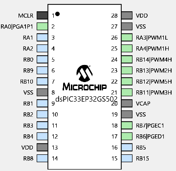
1.1.5 Where are all those PWM- and comparator pins in a dsPIC33EP32GS502 (SOIC-28) ?
On the first look into the datasheet, you wonder where those 5 * 2 PWM outputs
plus four comparator inputs can be found in a dsPIC33EP32GS502-I/SO:
Alternate pin functions (dsPIC33EP32GS502, similar for dsPIC33EP32GS202 with less on-chip peripherals) :
| Pin Nr |
Functions |
Notes |
|---|
| 1 | /MCLR | - |
| 2 | RA0,
AN0,PGA1P1,CMP1A | - |
| 3 | RA1,
AN1,PGA1P2,PGA2P1,CMP1B | - |
| 4 | RA2,
AN2,PGA1P3,PGA2P2,CMP1C,CMP2A | - |
| 5 | RB0,
AN3,PGA2P3,CMP1D,CMP2B,RP32 | - |
| 6 | RB9,
AN4,CMP2C,CMP3A,ISRC4,RP41 | - |
| 7 | RB10,
AN5,CMP2D,CMP3B,ISRC3,RP42 | - |
| 8 | Vss (digital GND) | - |
| 9 | RB1,
OSC1,CLKI,AN6,CMP3C,CMP4A,ISRC2,RP33 | - |
| 10 | RB2,
OSC2,CLKO,AN8,PGA1N2,CMP3D,CMP4B,RP34 | - |
| 11 | RB3,
PGED2,AN18,DACOUT1,INT0,RP35 | - |
| 12 | RB4,
PGEC2,ADTRG31,EXTREF1,RP36 | - |
| 13 | Vdd (+3V3) | - |
| 14 | RB8,
PGED3,SDA2,FLT31,RP40 | - |
| 15 | RB15,
PGEC3,SCL2,RP47 | - |
| 16 | RB5,
TDO,AN19,PGA2N2,RP37 | - |
| 17 | RB6,
PGED1,TDI,AN20,SCL1,RP38 | - |
| 18 | RB7,
PGEC1,AN21,SDA1,RP38 | - |
| 19 | Vss (digital GND) | - |
| 20 | Vcap | - |
| 21 | RB11,
TMS,PWM3H,RP43 | - |
| 22 | RB12,
TCK,PWM3L,RP44 | - |
| 23 | RB13,
PWM2H,RP45 | - |
| 24 | RB14,
PWM2L,RP46 | - |
| 25 | RA4,
PWM1H | - |
| 26 | RA3,
PWM1L | - |
| 27 | AVss (analog GND) | - |
| 28 | AVdd | - |
- ISRCxx : Constant Current Source
- The constant-current source module is a precision current generator
and is used in conjunction with the ADC module
to measure the resistance of external resistors
connected to device pins.
If you're also missing "ISRC1" in the above table:
"ISRC1" only appeared in a table for a 44-pin family member.
- PGED/C/1..3 : This "PG" doesn't mean "Programmable Gain" but "Programming/Debugging" !
- There are THREE communication channels for debugging/programming.
Each channel has two pins (e.g. "PGED"=Data, "PGEC"=Clock).
> Pull-up resistors, series diodes and capacitors on the
> PGECx and PGEDx pins are not recommended as they will
> interfere with the programmer/debugger communications
> to the device. If such discrete components are an application
> requirement, they should be removed from the circuit
> during programming and debugging. (...)
Which of those channels is enabled 'per default' from the factory,
and must be kept available for programming ? The datasheet
(DS70005127D page 282) says this is controlled by two "ICS"-bits
in the 'Configuration Words' in volatile(!) memory, loaded
from the 'Flash Configuration Words' during RESET.
As so often, the default values in those 'Flash Configuration Words'
couldn't be found anywhere in the datasheet.
> Unfortunately, I cannot find anywhere written the default value
> of these two Communication Channel Select configuration bits,
> so how do I know which of the three pairs of programming pins
> should I use with a fresh-from-factory device ?
Someone answered:
> The programming pair used is determined by the
> configuration bits in MPlab by default pair1 is set.
(Interesting. A fresh-from-the-factory device already knows
what you set "in MPlab". Harr harr.)
Someone else answered:
> Totally wrong.
> Any of the PGD/PGC pin pairs can be used for PROGRAMMING.
> Only the pair used for DEBUGGING must be selected
> via FICD nonvolatile configuration register bits.
The default configuration shown by MPLAB-X/MCC's
"Pin Manager"/"Package View" showed pin 18 (main function "RB7")
used as PGEC1
and pin 18 (main function "RB6") used as PGED1. Since this didn't steal
any of the precious non-remappable PWM outputs,
keep those settings.
Interestingly, when powering on the improvised "evaluation board"
after a previous debugger session, without a PICkit3 connected at all,
the dsPIC remained in some kind of waiting-for-the-debugger state
during which both PGEC1 and PGED1 were actively driven by the PIC
(bursts of 23 kHz squarewaves on PGEC1, repeated every 23 ms)
- which confirms the pin pair used for DEBUGGING is stored in a non-volatile
register. Remember this when running out of I/O pins: RB7 and RB6 may turn
into outputs unexpectedly.
- PWMxH,PWMxL : Outputs from the 'high-speed PWM'.
- THREE of those FIVE PWM units outputs (two per PWM) are NOT remappable,
and thus listed in the pin function table quoted above (PWM1,2,3).
A footnote in DS70005127D page 2 says:
> PWM4 and PWM5 are remappable on all devices except the 64-pin devices.
That's good news - in older devices, high-speed PWM outputs were never re-mappable.
1.2 The dsPIC33E's clock system
Because none of the functions automatically generated by MCC
worked properly (all the PWM outputs only produced 50 % of the frequencies "predicted" by MCC),
it was time to understand the details of the dsPIC33E's clock system (here: dsPIC33EP32GS502).
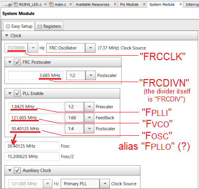
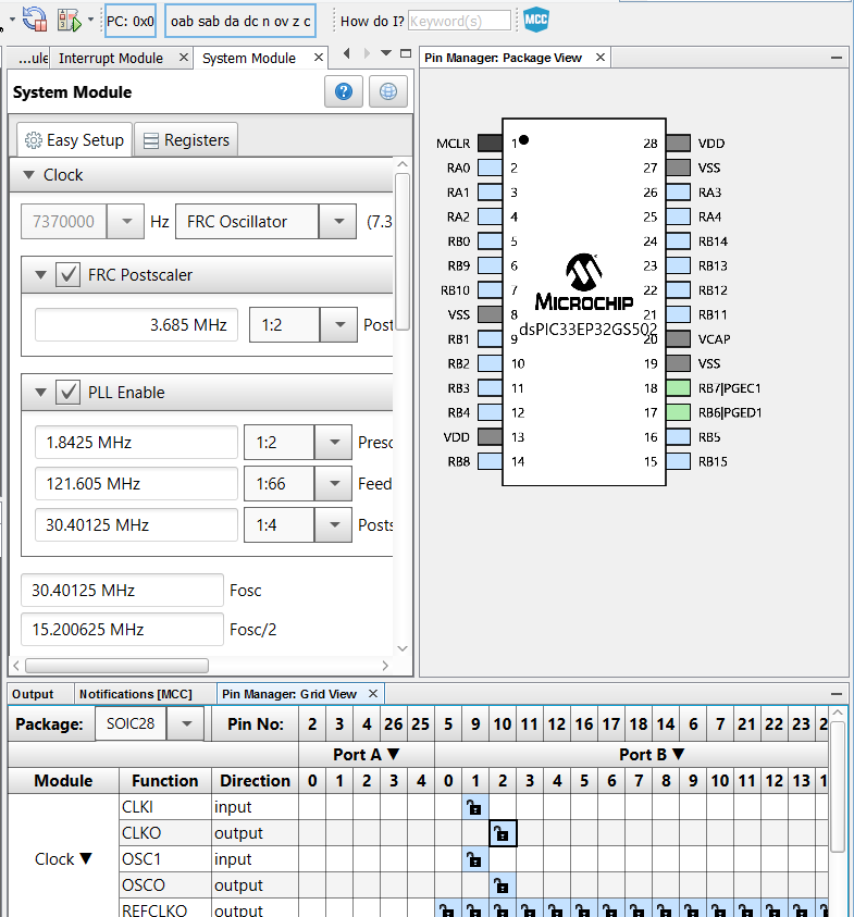
"System Module" / "Clock Setup" as shown in MPLAB X v4.54
Wondered what all those unlabelled frequencies shown in Mr. MCC's "Composer Area" were,
and what the official names of those signals are in the
datasheet.
The results were later added to the "MCC"-screenshot shown above
(red = additions by the author).
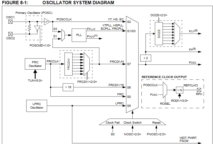
"OSCILLATOR SYSTEM DIAGRAM" from the dsPIC33EPXXGS50X family datasheet.
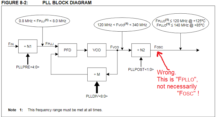
"PLL BLOCK DIAGRAM" from the dsPIC33EPXXGS50X family datasheet.
With the above, it becomes obvious that what "MCC" calls "Prescaler" are the five "PLLPRE"-bits,
"FeedBack" are the nine "PLLDIV"-bits, "Postscaler" is the two-bit "PLLPOST", and "FOSC" shown in
FIGURE 8-2 of the datasheet is plain wrong and should be labelled "Fpllo" instead (because
"FOSC" is the output of a giant multiplexer shown in FIGURE 8-1; it's not the output
of the main PLL.
1.2.1 The dsPIC33E's Oscillators
Initial tests with the improvised
dsPIC33EP32GS502 'eval board' used the internal 'FRC Oscillator' (Resistor-Capacitor),
but the high-speed PWM outputs exhibited strong jitter / phase noise
which could not be tolerated in a 'radio friendly' environment, so the
performance of the dsPIC33E's PLLs was also tested with a crystal on the PIC's
'Primary Oscillator' (in "Medium Speed Oscillator (XT) Mode"
for crystal frequencies from 3.5 to 10 MHz - see
DS70005131A page 21).
1.2.1.1 The dsPIC33E's 'FRC Oscillator'
In a dsPIC, "FRC" means Fast RC Oscillator. In a dsPIC33EPxxGS50x, with a bit of help
from our system initalisation code (*), Mr. "FRC" will produce 7.37 MHz with an accuracy
of -0.9 to +0.9 % between -10°C and 85°C. That's quite remarkable for an R-C-oscillator,
and would even be sufficient for a UART interface.
- About FRC Oscillator Tuning bits ("OSCTUN"):
- The dsPIC33 Family Family Reference Manual / "Oscillator"
(DS70005131a for dsPIC33EPxxGSxxx) tells us:
> The application software can tune the frequency of the oscillator
> using the FRC Oscillator Tuningbits (TUN<5:0>) in the FRC
> Oscillator Tuning register (OSCTUN<5:0>)
"Can" ? Doesn't sound like the PIC preset these bits with a 'factory calibration' !
For stoneage chips, a factory-calibrated value for "OSCCAL" could be read
from the last location in code space. Where is the equivalent for a dsPIC33 ?
The MCC-generated
stuff did this (in Blabla.X/mcc_generated_files/clock.c):
Ooops. There doesn't seem to be a FACTORY CALIBTRATION for Mr. FRC's frequency
- or is it the POWER-ON default value in "OSCTUN" ?
Maybe it's not in the "Family Reference Manual / Oscillator" but in the datasheet ?
DS70005127D page 28 mentions a few "DEVICE CALIBRATION ADDRESSES" (near 0x800E48)
but none of them was related with Mr. FRC. Conclusion/Guesswork: FRC is *not*
calibrated 'at the factory', so if we need it, we must calibrate Mr. FRC ourselves
and store the result in an EEPROM - if the dsPIC33E had an EEPROM.
To find the 'exact' frequency, the MCC configuration was temporarily
modified to "Clock Output Pin Configuration" : "OSC2 is clock output",
the test project rebuilt, downloaded ("Debug".."Debug Main Project"),
and the frequency on the dsPIC33EP32GS502's pin 10 (now labelled "CLKO") was measured.
Test result: DC current consumption rose from 37 to 40 mA,
and "CLKO" produced a square wave near 15.23 MHz
that suffered from phase noise (the jitter
made it impossible to "hear" to the signal
on a narrow-band receiver).
1.2.1.2 The dsPIC33E's 'Primary Oscillator'
A test with a widely available 7.3728 MHz crystal
(configured as "Primary Oscillator" in MCC's "System Module",
frequency manually entered instead of the 7.3700 MHz "FRC")
confirmed that most of the PWM output jitter was not caused by
the 'Auxiliary Clock' PLL
but by Mr. FRC himself. So, to avoid polluting the RF bands
with wobbly carriers all over the place, use a crystal oscillator
(or a crystal if you can sacrifice TWO pins) instead of Mr. "FRC".
Selecting the "Primary Oscillator" instead of "FRC Oscillator"
automatially disabled the "Reference Oscillator Output" in MCC. Ok.
The dsPIC33EP32GS502's auxiliary clock PLL (which multiples the
input clock by a fixed factor of 16) accepts input frequencies
between 7.0 and 7.5 MHz, with a "recommended" value of 7.37 MHz.
So the cheap 7.3728 MHz crystal should be fine for the AUX PLL
(and the high-speed PWMs fed from there), but what about a
"nice core clock" from this 'Primary Oscillator' frequency ?
We'll care about this later in the chapter about the
dsPIC33E's 'Main PLL'.
When using an external crystal, not an external crystal oscillator,
"OSC2" (which MPLAB/MCC calls "OSCO" just to confuse you) must be
actively driven. From system.c:
// FOSC
#pragma config POSCMD = XT    // Primary Oscillator Mode Select bits->XT Crystal Oscillator Mode
#pragma config OSCIOFNC = ON  // OSC2 Pin Function bit->OSC2 is general purpose digital I/O pin VERY MISLEADING ! See WB's notes below.
#pragma config IOL1WAY = ON   // Peripheral pin select configuration bit->Allow only one reconfiguration
#pragma config FCKSM = CSECME // Clock Switching Mode bits->Clock switching is enabled,Fail-safe Clock Monitor may be on
#pragma config PLLKEN = ON    // PLL Lock Enable Bit->Clock switch to PLL source will wait until the PLL lock signal is valid
From DS70005131A page 40, chapter 14.0, "Clock Switching":
Clock switching can be initiated
as a result of a hardware event or a software request. A typical scenario includes:
- Two-Speed Start-up sequence upon Power-on Reset, which initially
uses the Internal FRC Oscillator for quick start-up
and then automatically switches to the selected clock source
when the clock is ready.
- Fail-Safe Clock Monitor automatically switches to the Internal
FRC Oscillator on a clock failure.
- User-assigned application software requests clock switching
by setting the OSWEN bit (OSCCON<>),
causing the hardware to switch to the clock source selected by
the NOSC<2:0> bits (OSCCON<10:8>) when the clock is ready.
In each of these cases, the clock switch event assures that
the proper make-before-break sequence is executed.
That is, the new clock source is ready before the old clock
is deactivated and code continues to execute as clock switching
occurs.
dsPIC33/PIC24 family devices feature the Phase-Locked Loop Enable (PLLKEN)
bit in the Oscillator Configuration register (FOSC<8>).
Setting this bit will cause the device to wait until the PLL
locks before switching to the PLL clock source.
When this bit is set to '0', the device will not wait for the PLL lock
and will proceed with the clock switch. The default setting for this
bit is '1'.
Ok, so we may start "quickly" in FRC mode, then fire up the "Primary Oscillator"
in "XT"-mode (how.. is there an alternative to the fixed "Fuse Bits"?),
check if that oscillator REALLY runs, then feed that signal
into the PLL, and finally switch "Fosc" (with the double core frequency) to "Fpllo".
1.2.2 The dsPIC33E's 'Main PLL' (feeding the 'core')
The "core clock" (called "FCY" in figure 8-1) is HALF of "FOSC" or even less, depending on the
power-saving "DOZE"-bits (allows running the microprocessor on a lower frequency but keeping
the on-chip peripherals running at full speed).
To check the main PLL configuration (when fed from "FRC"),
configured pin 10 as "REFCLKO", check "Reference Oscillator Output" on the
"System Module" tab, set "Reference Clock Source Select" to "FOSC",
set "Reference Clock Divider" to 0x0 -> MCC says there should be
30401250 Hz on "REFCLKO". Rebuild project, download, measure again... Result:
30.474 MHz on "REFCLKO", same jitter as from "CLKO".
With the main PLL reconfigured for Fvco=243.21 MHz, Fpllo=60.8 MHz,
Fosc=Fpllo, Fcyc=Fosc/2=30.4 MHz:
DC current consumption rose to 60 mA (!), and the frequency
measured on "REFCLKO" was 60.490 MHz with a lot of jitter.
To tame the jitter and get reproducable results, the FRC oscillator
was later replaced by a 7.3728 MHz crystal (on the "Primary" oscillator
in "XT" mode). DS70005127D
presents a formula for the main PLL frequencies on page 105:
                        PLLDIV + 2
 FPLLO = FPLLI * ----------------------------
                2 * (PLLPRE+2) * (PLLPOST+1)
                 PLLDIV + 2
 FVCO = FPLLI * --------------
                 PLLPRE + 2
Example 1:
FPLLI = 7.3728 MHz,
PLLDIV (nine-bit-group value in "PLLFBD") = 64
PLLPRE (five-bit-group value in "CLKDIV") = 0
PLLPOST (two-bit-group value in "CLKDIV") = 0
-> FPLLO = 7.3728 MHz * (64+2) / ( 2 * (0+2) * (0+1) ) = 121.6512 MHz (measured: 121.6646 MHz, ok, 110 ppm "off")
and FVCO = 7.3728 MHz * (64[PLLDIV]+2) / (0[PLLPRE]+2) = 243.3024 MHz (ok)
Example 2 (closer to the intended "60 MIPS") :
FPLLI = 7.3728 MHz,
PLLDIV (nine-bit-group value in "PLLFBD") = 226
PLLPRE (five-bit-group value in "CLKDIV") = 5
PLLPOST (two-bit-group value in "CLKDIV") = 0
-> FPLLO = 7.3728 MHz * (226+2) / ( 2 * (5+2) * (0+1) ) = 120.071 MHz
and FVCO = 7.3728 MHz * (226[PLLDIV]+2) / (5[PLLPRE]+2) = 240.143 MHz (ok)
Example 3 (same frequency from the MAIN PLL as from the AUXILIARY PLL, Fin * 16):
FPLLI = 7.3728 MHz,
PLLDIV (nine-bit-group value in "PLLFBD") = 62
PLLPRE (five-bit-group value in "CLKDIV") = 0
PLLPOST (two-bit-group value in "CLKDIV") = 0
-> FPLLO = 7.3728 MHz * (62+2) / ( 2 * (0+2) * (0+1) ) = 117.965 MHz
and FVCO = 7.3728 MHz * (62[PLLDIV]+2) / (0[PLLPRE]+2) = 235.9296 MHz (ok)
1.2.3 The dsPIC33E's 'Auxiliary Clock Generator'
The clock source for the High-Speed PWMs cannot be seen in
the part of figure 8-1 (-> dsPIC33EP32GS502 datasheet
DS70005127D page 104). Only the lower half (with the "Auxiliary Clock Generator Circuit Block Diagram")
shows a clock signal named "ACLK" being routed to the PWM, ADC, and LFSR. Isn't it possible to feed the
(HS-)PWM from the main PLL ? As often, we're not alone, someone else stumbled across exactly the same
omission in the data sheet:
> I have recently shifted to dsPIC33EPXXGSXX50X.
> I am unable to find, how to select the Clock source
> for the high-speed PWM module.
> In the ref manual the register description, talks about
> SYNCX input but nothing about the clock source.
Hmm.. this is what the dsPIC33EPxxGS50x datasheet had to say IN CHAPTER AUXILIARY CLOCK GENERATION,
not in chapter HIGH-SPEED PWM:
> To achieve 1.04 ns PWM resolution, the auxiliary clock must use
> the 16x Auxiliary PLL (APLL). All other clock sources will have
> a minimum PWM resolution of 8 ns.
Details about the HS PWM were only in the "dsPIC33/PIC24 Family Reference Manual"
/ "High Speed PWM" (DS70000323H) which tells us:
The auxiliary clock generator must be used to generate the clock
for the PWM module independent of the system clock.
Ok, and what if we don't need a "PWM clock independent of the system clock" ? No answer to this.
But, as already speculated in various forums, the Auxiliary PLL's fixed multiply-by-SIXTEEN
may be the key to the advertised "1.04 ns" resolution of the PWM, and thus NO OTHER POSSIBLE CLOCK SOURCE.
So, taking the info from DS70000323H for granted, the ACLK feeding the (HS-)PWM is:
Equation 5-1:ACLK Frequency Calculation

   Where:
     REFCLK=  Internal FRC clock frequency (7.37 MHz) if the Internal FRC
              is selected as theclock source
         or
     REFCLK=  Primary Oscillator Clock (POSCCLK) frequency if the
              Primary Oscillator(POSC) is selected as the clock source
     M1 =  16, if the auxiliary PLL is enabled by setting the ENAPLL bit (ACLKCON<15>)
         or
     M1 =  1,  if the auxiliary PLL is disabled
     N  =  Postscaler ratio selected by the Auxiliary Postscaler bits (APSTSCLR<2:0>)
           in the Auxiliary Clock Control register (ACLKCON<2:0>)
Clock Source: FRC (not "Primary Oscillator", not "Primary PLL"),
PLL Enable: checkmark also SET, multiplies the 7.37 MHz by 16 -> 117.92 MHz,
Postscaler: 1:1,
the HS PWM finally seemed to work.
But due to the incredible phase noise from Mr. "FRC", the "Auxiliary Clock"
input frequency was later replaced by jitter-free 7.3728 MHz crystal
driven by the primary oscillator,
so the auxilary oscillator's PLL produced a low-jitter 16 * 7.3728 MHz = 117.9648 MHz
for both the HS-PWM as well as the HS-ADC.
1.2.4 dsPIC33EP32GS502 current consuption (measured) with different clock setups
For quick tests, MCC was used to generate
the initialisation code, with resulting clock frequencies shown in the table below.
The 'REFCLKO' output was sometimes enabled on RB2, without 'Reference Clock Divider'.
Frequencies measured on 'REFCLKO' are shown under FREFCLKO.
FACLK is the frequency of the 'Auxiliary Clock' (shown as "ACLK"
in the datasheet, figure 8-1, "AUXILIARY CLOCK GENERATOR CIRCUIT BLOCK DIAGRAM").
Since it seemed impossible to route FACLK to 'REFCLKO', it was either
concluded from the PWM output frequency or taken for granted from MCC (under
'System Module', 'Auxiliary Clock').
The DC current consumption was measured on the improvised
dsPIC33EP32GS502 'eval board' with 3.3 V on Vdd and AVdd.
In all cases, the FRC (with approx. 7.37 MHz) was the source
for all clocks (main and auxiliary).
As in the planned application, all five HS PWMs were enabled and "producing output".
| FPLLI |
FVCO |
FPLLO |
FOSC |
FREFCLKO |
FCY (theor.) |
FACLK |
DC current |
Notes |
|---|
| 3.685 MHz | 243.21 MHz | 60.8025 MHz | 60.8025 MHz | 60.95 MHz | 30.401 MHz | 117.92 MHz | 48 mA | |
| 3.685 MHz | 243.21 MHz | 121.605 MHz | 121.605 MHz | 121.9 MHz | 60.8025 MHz | 117.92 MHz | 69 mA | (1) |
| 3.685 MHz | 243.21 MHz | 121.605 MHz | 121.605 MHz | disabled | 60.8025 MHz | 117.92 MHz | 58 mA | |
Conclusions / Notes:
- (1) Feeding 'REFCLKO' with high frequencies is a bad idea, and draws a lot of extra current
- Electrical Characteristics (esp. supply currents) must be taken with a grain of salt
- Read the data sheet, and don't assume MCC will inform you about violating the specs !
1.3 The dsPIC33E's Serial Peripheral Interface
To drive a minature 1.8" TFT display with a
dsPIC33EPxxGS502,
a 'software' SPI master was tried initially. It worked right out of the box, but
without highly optimized C (XC16 "free edition", no manually unrolled loops)
or even hand-crafted assembler, the achieveable SPI clock frequency was only 2.5 MHz,
while the dsPIC core was melting away at "60 MIPS".
The external TFT controller (one of the many ST7735 flavours) allowed a
"Serial Clock Cycle (Write)" of 66 ns, and a
"Serial Clock Cycle (Read)" of 150 ns, e.g. 15 MHz to write, and 6 MHz to read
pixel data via SPI.
- Note:
- The Sitronix ST7735S datasheet calls the serial interface lines
"SDA" and "SCL" which sounds like I2C, but it's in fact SPI with
a funny bi-directional data line. More on that, and how
to make the 'SDA'-line bi-directional again on certain 5-Volt tolerant
'Arduino display adapter boards' may still be
here
(description of a project with a dsPIC and one of these displays).
Can the dsPIC33EP's hardware "SPIx Module" (x=1..2) be convinced to route
both "SDOx" and "SDIx" to a common pin (without sacrificing two pins) ?
As usual, the dsPIC33EPxxGS502 datasheet (DS70005127D page 207) suggests
to read details in the Familiy Reference Manual, in this particular case in
DS70005185A (again, saved locally
in the 'datasheets' folder).
But there's no bi-directional operation of the dsPIC33-SPI's data line,
and the "TX Only in Master mode" + "RX Only in Master mode"
mentioned in DS70005185A on page 33 only applies to the DMA, not to a "pin".
To write to and read from the ST7735 through only
one data line ("SDA"),
try to map the dsPIC-SPI's "SDOx" (aka MOSI) and "SDIx" (MISO)
to the same pin ?
More details in
file:///C:/pic/dsPIC33EP32GS502_RGBW_LED_SMPSU/dsPIC33EP32GS502_Drivers/iop.c.
1.4 The dsPIC33E's different (and very incompatible) ADC flavours
When, for various reasons, switching from a dsPIC33EPxxGS502 to a dsPIC33EPxx(x)MC502, it quickly
became obvious that the code originally written for the 'GS' ("digital power") family was utterly
incompatible with the 'MC' ("motor control") family. So beware, even if two devices sound
similar (like dsPIC33EP64GS502 vs dsPIC33EP64MC502), their on-chip peripherals may be
very different. Here's a list of A/D converters seen so far, with the full document titles,
a few particular devices containing them, and links to the relevant parts of the 'FRM'
(Family Reference Manual):
- '12-Bit High-Speed, Multiple SARs A/D Converter (ADC)' in DS70005213G:
That's the ADC present in dsPIC33EP16/32/64GS502/504/505/506 .
Has FIVE Sample&Hold circuits for 12 bit resultion,
and can thus simultaneously digitize FIVE analog inputs at up to 3.25 MSamples/second
(but as usual, these promises must be taken with a gain of salt).
Since the entire document (DS70005213G) never mentions the term 'DMA',
this really-high-speed A/D converter will cause a lot of CPU load
when used to digitize gapless streams of samples. Taking the overhead of
interrupt latencies into account, even at 70 "MIPS" (maximum core speed) you cannot
do a lot of DSPing if those "3.25 Msps" shall form a gapless stream of samples (w/o DMA).
- 'Section 16. Analog-to-Digital Converter (ADC)' in DS70621C:
That's a very different ADC used in dsPIC33EP32/64/128/256/512MC502/504/505/506 .
Those 'MC' (Motor Control) chips only contain ONE of these ADCs,
and when configured for 12 bit resolution, can only digitize ONE analog input
at a time (because there's only ONE Sample&Hold circuits at 12 bit resultion).
It's hard to understand why FOUR Sample&Hold circuits (and thus FOUR simultaneously
digitized inputs) are only possible at 10 bit resolution.
But, in contrast to the more versatile ADC described in DS70005213G,
this particular ADC may be connectable to DMA
if the particular chip supports DMA (the dsPIC33EP32/64/128/256/512MC502 does),
making it more suitable for continuous digital signal processing at higher
sampling rates (if there wasn't this crazy ONE-CHANNEL limit at 12 bit resolution).
In short, if the datasheet references to DS70621, forget about
simultaneously sampling multiple channels with 12 bit resultion. At 12 bit,
up to 500 kSamples/second are ok, nothing more. Oh well, but thank you for the DMA.
Note: Code Example "CE422" seems to be suited for THIS kind of ADC and DMA.
But beware of the camouflaged definition of the '#pragma configs' in "adcdrv1.c",
where they really don't belong. Also, the definition of "Message Buffer Lengths
for ECAN1/ECAN2" really doesn't belong there - another case of
brainless block-copying .. the DMA part stolen from a CAN bus driver ?
1.4 dsPIC33E (newer) versus dsPIC33F (older)
Pro-dsPIC33E (newer), contra-dsPIC33F (older):
- When running at the same core clock (e.g 40 "MIPS"),
a dsPIC33E consumes significantly less power than a dsPIC33F:
dsPIC33EP32GS502 : typ. 51 mA at 70 MIPS with 5 PWMs on at full speed (page 306, DC27a)
(this could not be confirmed by own measurements, though. Details here)
dsPIC33FJ16GS502 : typ. 125 mA at 40 MIPS with PWM(s?) at max speed (page 290, DC25a)
- For the same on-chip peripheral, electrical data have been
improved for the dsPIC33E. Example: Offset voltage of the 'High-Speed Comparators':
dsPIC33EP32GS502 : Input Offset Voltage = -35mV ... +35mV
dsPIC33FJ16GS502 : Input Offset Voltage = -58mV ... +66mV (too much when directly fed from a hi-current shunt)
Pro-dsPIC33F (older), contra-dsPIC33E (newer):
- Lower interrupt call-and-return latency:
6 cycles on the "old" dsPIC33F (+), 19 cycles on the "new" dsPIC33E (--).
- dsPIC33F is often available in homebrew-friendly 28-pin Standard DIL.
dsPIC33E usually only avalilable in SOIC-28 or less homebrew-friendly cases.
(One exception is e.g. dsPIC33EP512MC502-I/SP : 28-pin Standard DIL
with 'a lot' of punch and memory, but just a single, not-so-capable ADC)
Pro-PIC16Fxx(x(x)), contra-dsPIC33 (E,F):
- dsPIC33E can only source/sink a maximum of 5 mA per pin.
Stoneage PICs had stronger output drivers, and could easily drive
multiplexed 7-segment displays without any transistor/driver.
1.5 Low power design with PIC16 / PIC18
This chapter may apply to more complex families like dsPIC33, and other
families with what Microchip calls "nanoWatt XLP" (extreme low power).
The PIC16(L)F1847 is a relatively modern successor for the once-popular
PIC16F628A. Both are still available in homebrew friendly 18-pin standard
DIL (through-hole, non-SMD), nice for solderless 'breadboard' prototyping.
Even the 20-year old PIC16F628A is advertised as "nanoWatt Technology",
with this summary of low-power features (in the datasheet):
- Standby Current:
- 100 nA @ 2.0V, typical
- Operating Current:
- 12 uA @ 32 kHz, 2.0V, typical
- 120 uA @ 1 MHz, 2.0V, typical
- Watchdog Timer Current:
- 1 uA @ 2.0V, typical
- Timer1 Oscillator Current:
- 1.2 uA @ 32 kHz, 2.0V, typical
- Dual-speed Internal Oscillator:
- Run-time selectable between 4 MHz and 48 kHz
- 4 us wake-up from Sleep, 3.0V, typical
In a breadboard with a PIC16F628A, the following total supply
currents were measured (flowing into the PIC through pin 14 = Vdd):
Clock
source | Fcore | Vdd | Idd
(measured) | Other Conditions, remarks |
|---|
| INTOSC | 4 MHz | +5.0 V | 770 uA | No 'Sleep with Timeout' |
| INTOSC | 4 MHz | +3.6 V | 605 uA | No 'Sleep with Timeout' |
| INTOSC | 4 MHz | +5.0 V | 7 uA | 2.2(!) s 'Sleep with Timeout' |
| INTOSC | 4 MHz | +3.6 V | 3 uA | 2.5(!) s 'Sleep with Timeout' |
| INTOSC | 48 kHz | +5.0 V | 154 uA | No 'Sleep with Timeout' |
| INTOSC | 48 kHz | +3.6 V | 137 uA | No 'Sleep with Timeout' |
| INTOSC | 48 kHz | +5.0 V | 7 uA | 2.2(!) s 'Sleep with Timeout' |
| INTOSC | 48 kHz | +3.6 V | 3 uA | 2.5(!) s 'Sleep with Timeout' |
| INTOSC | 48 kHz | +3.6 V | < 1 uA | 'Sleep WITHOUT Timeout', WDT off |
DC current consumptions measured with a PIC16F1847.
Conditions for all measurements in the table above:
Analog comparators off, Watchdog timer enabled (for the periodic wake-up),
Brown-Out-Detector/Reset off (to run at 3 .. 3.6 V),
Conclusions from the above measurements with a PIC16F628A:
- There is no proportional relation between clock frequency and current consumption:
Fclk_hi/Idd = 770 uA / 4 MHz = 192 uA per MHz
Fclk_lo/Idd = 154 uA / 48 kHz = 3208 uA per MHz
- → If there's significant "work to do", let the PIC16F628A
run at 4 MHz, not at 48 kHz (both from 'INTOSC').
After "work is done", go to sleep again much earlier
than if the job was done at the low core clock frequency.
- A single misconfigured digital input, with the level allowed to 'float',
lets the power consumption increase by a hundred microamperes !
This can easily be checked by subsequently touching all pins of
the PIC (also the "unused ones") with a high-impedance source
delivering the half supply voltage, e.g. a resistive
voltage divider from two 1-MOhm resistors.
- The WDT (Watchdog Timer) oscillator isn't as precise as the 4 MHz "INTOSC".
- The PIC16F628A's 4 MHz "INTOSC" frequency is more precise than the
"INTOSC" in "low speed" mode (48 kHz for PIC16F628A, 30..31 kHz for PIC16F1847).
- "Sleeping with periodic wake-up per WDT"
finally consumed the expected current (based on the PIC16F628A datasheet):
- DS40044G page 138 specifies a "Power-down Base Current (IPD)" of 0.85 uA (typ) at Vdd=3.0 V
- DS40044G page 138 specifies a "Peripheral Module Current (deltaImod)" for the WDT of 2 uA (typ) at Vdd=3.0 V
Total (IPD + deltaImod_WDT) = 0.85 uA + 2.0 uA = approximately 3 uA, as measured.
- With a 0.5 Ah 3.6 V LiIon cell, ignoring the self discharge, that's sufficient for
(0.5 Ah / 3 uA) / (24*365) = 19 years of operation
- assuming the CPU's duty cycle (ratio of "working" to "sleeping") is
as low as e.g. in a smoke detector, low duty cycle "Microwave beacon", etc.
For comparison: The "Supply current in standby-I mode" of an nRF24L01+
is 26 uA ("Standby-I mode" of this 2.4 GHz transceiver is used to minimize
average current consumption while maintaining short start up times." ).
Thus even when neither receiving nor transmitting, an nRF24L01+ consumes
more battery current than a 'mostly sleeping PIC'.
Later, when the PIC16F628A's Flash and RAM got too small for a more demanding application,
the experiment described above was repeated with a modern but pin-compatible successor,
the PIC16F1847 (also not the 'L' type). Only the 'standby' current consumption was of interest.
Here, periodic wake-up was achieved via Watchdog Timer (sometimes the datasheet
calls this watchdog "WDT", sometimes "LPWDT", but in fact there is only one WDT),
clocked by the PIC16F1847's "LFINTOSC" (nominal frequency = 31 kHz, even though the datasheet often says
"Fosc=32 kHz" when using "LFINTOSC"). The same oscillator ("LFINTOSC") can also be used
as direct CPU clock - this was used for some of the tests below.
Clock
source | Fcore | Vdd | Idd
(measured) | Other Conditions, remarks |
|---|
| INTOSC | 4 MHz | +5.0 V | 735 uA | No 'Sleep with Timeout' |
| INTOSC | 4 MHz | +3.6 V | 730 uA | No 'Sleep with Timeout' |
| INTOSC | 4 MHz | +5.0 V | __ uA | 2.xx s 'Sleep with Timeout' |
| INTOSC | 4 MHz | +3.6 V | 12 uA | 2.18 s 'Sleep with Timeout' |
| LFINTOSC | 31 kHz | +5.0 V | 17 uA(!) | No 'Sleep with Timeout' |
| LFINTOSC | 31 kHz | +3.6 V | 17 uA(!) | No 'Sleep with Timeout' |
| LFINTOSC | 31 kHz | +5.0 V | __ uA | 2.xx s 'Sleep with Timeout' |
| LFINTOSC | 31 kHz | +3.6 V | _ uA | 2.xx s 'Sleep with Timeout' |
| LFINTOSC | 31 kHz | +3.6 V | _ uA | 'Sleep WITHOUT Timeout', WDT off |
DC current consumptions measured with a PIC16F1847 (not PIC16LF1847!)
- Note:
- While sleeping with periodic wake-up, that's 12 uA with a PIC16F1847 versus 3 uA with a PIC16F628A.
But while "working" with f_core=31 kHz, the PIC16F1847 draws less current than a PIC16F628A at a similar speed.
2. Notes about developing with MLPAB-X
Unfortunately Microchip have replaced the blazingly fast, highly responsive
"MPLAB" (e.g. MLPAB V8.x) by the Java/Netbeans-based bloat known as "MPLAB-X".
But since the old MPLAB never could keep sourcecode and execution point
in sync during debugging (when "stepping into" any function or subroutine),
take your sleeping pill and install the 1.1 GByte installer (anno 2021) for the IDE.
Next, also install the C compiler (e.g. the poor, non-optimizing "free" XC16 for
PIC24 and dsPIC30/33). The performance of the "free" compiler was a bad joke
("you could have produced much smaller and much faster code if you BOUGHT our compiler"),
but anyway ... we'd use an ARM-Cortex for more demanding applications, not a PIC.
Snippets / solutions for shortcomings of MPLAB X:
- How to open the map file from the IDE ? Where to find it ?
Since there is no simple item like 'Open map file' in the 'File'
menu as in other IDEs for embedded firmware development,
ask your favourite file manager for a file with extension *.map.
If you're lucky, it's already there - but don't bet on it.
The option to generate it, and path to the map file can be found in MPLAB X under
'Project Properties'..'XC16'..'xc16-ld'..
Option Categories : Diagnostics..
Generate map file.
The default setting was something like this ...
${DISTDIR}/${PROJECTNAME}.${IMAGE_TYPE}.map
.. resulting in a map file buried deep inside the project folder, e.g.
C:\pic\dsPIC33EP_Si5351_Synth\dsPIC33_Si5351_Synth.X\
dist\default\production\dsPIC33_Si5351_Synth.X.production.map
2.1 The hassle with MPLAB-X include file paths for the C compiler
Quoted from another frustrated MPLAB-X user:
> My main.c file knows where my #include "StdTypes.h" file is
> and has no problems with it, but the mcc_generated_files tmr0.c file
> can't find it. Why is that?
>
> I do not understand, when you set up a project and tell it
> where your files are, that it is not smart enough
> to find those files. This is my first time working
> with MPLAB X IDE and I am finding it to be a pain to work with.
The solution in this incredibly brain-damaged IDE is that you don't
only need to add the path via
File .. Project Properties .. General .. Source Folders .. Add
but instead those folders must also be added under
File .. Project Properties .. XC16 .. xc16-gcc ..
.. Option categories:"Preprocessing and messages" .. C include dirs ..
.. "..."[button] .. "Browse" .. etc, find your way to the folders with all your include files.
If the target is an 8-bit PIC like PIC10/12/16, the compiler is XC8,
and to get to the compiler's list of include paths, select...
File .. Project Properties .. XC8 Global Options .. XC8 Compiler ..
.. Option categories:"Preprocessing and messages" .. Include directories ..
2.2 Predefined symbols for the C compiler (stored in the MPLAB-X project ?)
When compiling the same application for different targets (e.g. dsPIC33EPxx, dsPIC33FJxx),
the current target CPU can be identified via preprocessor in "C".
Microchip's own "XC.H" floats around in dozens of incarnations in the deeply nested
'MPLAB X' installation folder, e.g.
C:\tools\Microchip\MPLAB_X_V545\packs\Microchip\dsPIC33E-GS_DFP\1.3.91\xc16\support\generic\h\xc.h
.
That's only the "XC.H" for a certain family of devices - there is no "universal" XC.H !
Each XC.H contains the names of pre-defined preprocessor macros identifying the target,
e.g.:
#if defined(__dsPIC33EP32GS502__)
#include <p33EP32GS502.h>
#endif
The symbol itself -without underscores- is possibly taken from the MPLAB-X "nbproject/project.xml",
from project.configuration.data.name (value e.g. "dsPIC33EP32GS502"), and passed
to the compiler via an incredibly long command line string, e.g.:
"C:\tools\Microchip\xc16v161\bin\xc16-gcc.exe" RGBW_LED.c -o build/default/production/RGBW_LED.o -c -mcpu=33EP32GS502 -MP -MMD -MF "build/default/production/RGBW_LED.o.d" -mno-eds-warn -g -omf=elf -DXPRJ_default=default -legacy-libc -msmall-code -msmall-data -msmall-scalar -O1 -I"../" -I"../switches_v1" -msmart-io=1 -Wall -msfr-warn=off -mdfp="C:/tools/Microchip/MPLAB_X_V545/packs/Microchip/dsPIC33E-GS_DFP/1.3.91/xc16"
The C compiler seems to reconstruct the full name ("dsPIC33EP32GS502")
from the the command line argument "-mcpu=33EP32GS502".
Warum einfach, wenn's auch kompliziert geht.
2.3 MPLAB "Code Configurator" ("MCC") ? Give it a try - but only for the initialisation
Someone suggested somewhere to use the 'MPLAB Code Configurator' (plugin)
to let this graphic tool generate the (initialisation-) code for a particular
device, and a given configuration of the on-chip peripherals "automatically".
Being sceptical about the quality of tools by Microchip, the author decided
to give it a chance for the projected multi-PWM 'RGBW driver'.
In "MPLAB X IDE v5.45", select "Tools" .. "Plugins" .. "Installed".
If there's no "MPLAB(R) Code Configurator" yet, look for it under
"Available Plugins", check it for installation, click "Install",
"accept", "Install", and go to have another cup of tea, then restart MPLAB-X.
A blueish "MCC"-icon appears somewhere (near "How do I?") in the GUI.
Click it. The plugin immediately asks "Save MCC Configuration File" before
you had the chance to set/modify anything. Oh well, let it save the default
"MyConfig.mc3" in your project folder. The currently opened project
must have the correct target (CPU) already selected before this step.
After installing and starting Microchip's "MCC", tried to let that tool
generate at least the initialisation code...
Screenshot of MPLAB-X's "MCC" (MPLAB Code Configurator)
Begin configuring the "System Module" with 'Clock', e.g.:
- Clock: 'FRC Oscillator' with 7.37 MHz, because the dsPIC33EP32GS502's
1.04 ns PWM resolution won't work with any other source-frequency (?)
- PLL: Must be enabled to generate ~~120 MHz for the PWM from the 7.37 MHz 'FRC'
- Auxiliary Clock: Enabled, source = "Primary PLL", 121.605 MHz, don't divide.
- CLKI, CLKO: Both OFF to use RB1 and RB2 as something else (I/O or PWM)
Also, from the MCC's "Available Resources" list, pick the following (click on [+]):
- PGA1: At least ONE programmable gain amplifiers will be used
for the current sensor (shunt resistor with a few hundred millivolts).
First attempt: Input on pin 2 = PGA1P1, gain approximately 3.3 V (ref) / 0.2 V = 16.
- PWM: Possibly ALL FIVE of them will be used (one as common current source,
four to shunt the LED's R,G,B,W component). After adding it,
rename the 'Custom Names' on the new 'PWM'-tab
(e.g. PWM_Main, PWM_Red, PWM_Green, PWM_Blue, PWM_White).
For PWM_Main, "Primary Master Time Base" Period = 0xFFFF gave a "Generator Period" of 67.3728 us,
that's 14.625 kHz -> insufficient.
"Primary Master Time Base" Period = 0xFFF -> 237107 Hz PWM frequency, ok.
For PWM_Red/Green/Blue/White, use "Duty Cycle Mode"=PRIMARY,
"Independent Time Base Mode"=PRIMARY, Edge Aligned, "Primary Phase Shift"(?!)=0x7FFF
-> Generator Period = 33.69 us ~~ 29682 Hz.
How to 'free' the unused PWMxL outputs for PWM_Red/Green/Blue/White ?
It's not under the PWM's "I/O Control" but in the "Pin Manager: Grid View" tab !
PWM4 and PWM5 could be mapped to almost any pin of "Port B" (except those already
occupied by PWM2H on RB13 and PWM3H on RB11), so let's assign..
PWM4H to RB14 -> pin 24 in the "Package View" turns green
PWM5H to RB12 -> pin 22 in the "Package View" turns green
But, as already expected, the result of the MCC-generated code was poor
(see notes from VK3RDB further below):
- PWM_Main: Measured generator frequency was 129 kHz, not 237 kHz as predicted by "MCC"
- PWM_Red..White: Measured 14.88 kHz, predicted 29.7 kHz
-> both frequencies only 50 % of the 'predicted' value.
Time to read datasheets and understand the dsPIC33E's clock system,
especially for beasts like the High-Speed-PWM !
The meaning of dsPIC33E-"High-Speed"-PWM-related fields in MCC,
and where to find the relevant information in the data sheets
is listed in chapter High-Speed PWM setup via MCC.
- Pin Manager: Unlike the more advanced functions (like PWM clocks),
the "Pin Manager: Grid View" seems to work properly.
When done with it, the results appear in the "Package View"
as shown further below.
Screenshot of MPLAB-X's "MCC" after assigning debugger- and PWM pins
From eevblog, by VK3DRB:
> STOP PRESS: I found the root cause of the problem:
> I used Microchip's Code Configurator. How utterly silly of me.
> It will be faster for me to write the code the old way,
> reading the datasheet.
So before getting over-enthusiastic about MCC, let's let it generate some code
and see what "pours out". On the left side of the window, tab "Resource Management (MCC)",
there are three buttons: "Generate", "Import..", "Export". Click 'Generate'.
The "MPLAB(R) Code Configurator" showed what was going on:
23:20:29.083    INFO: Saved configuration to file C:\pic\dsPIC33EP32GS502_RGBW_LED_SMPSU\dsPIC33EP32GS502.X\MyConfig.mc3
23:20:31.109    INFO: *****************************************************
23:20:31.110    INFO:  Generation Results
23:20:31.110    INFO: *****************************************************
23:20:31.148    INFO: main.c                                    Success. New file.
23:20:31.148    INFO: mcc_generated_files\clock.c               Success. New file.
23:20:31.149    INFO: mcc_generated_files\clock.h               Success. New file.
23:20:31.149    INFO: mcc_generated_files\interrupt_manager.c   Success. New file.
23:20:31.149    INFO: mcc_generated_files\interrupt_manager.h   Success. New file.
23:20:31.149    INFO: mcc_generated_files\mcc.c                 Success. New file.
23:20:31.149    INFO: mcc_generated_files\mcc.h                 Success. New file.
23:20:31.150    INFO: mcc_generated_files\pga1.c                Success. New file.
23:20:31.150    INFO: mcc_generated_files\pga1.h                Success. New file.
23:20:31.150    INFO: mcc_generated_files\pin_manager.c         Success. New file.
23:20:31.150    INFO: mcc_generated_files\pin_manager.h         Success. New file.
23:20:31.151    INFO: mcc_generated_files\pwm.c                 Success. New file.
23:20:31.151    INFO: mcc_generated_files\pwm.h                 Success. New file.
23:20:31.151    INFO: mcc_generated_files\pwm_module_features.h Success. New file.
23:20:31.151    INFO: mcc_generated_files\reset.c               Success. New file.
23:20:31.151    INFO: mcc_generated_files\reset.h               Success. New file.
23:20:31.152    INFO: mcc_generated_files\reset_types.h         Success. New file.
23:20:31.152    INFO: mcc_generated_files\system.c              Success. New file.
23:20:31.152    INFO: mcc_generated_files\system.h              Success. New file.
23:20:31.152    INFO: mcc_generated_files\system_types.h        Success. New file.
23:20:31.152    INFO: mcc_generated_files\traps.c               Success. New file.
23:20:31.152    INFO: mcc_generated_files\traps.h               Success. New file.
23:20:31.153    INFO: mcc_generated_files\watchdog.h            Success. New file.
23:20:31.207    INFO: *****************************************************
23:20:31.207    INFO:  Generation complete (total time: 2113 milliseconds)
23:20:31.207    INFO: *****************************************************
23:20:31.207    INFO: Generation complete.
23:20:31.345    INFO: Saved configuration to file C:\pic\dsPIC33EP32GS502_RGBW_LED_SMPSU\dsPIC33EP32GS502.X\MyConfig.mc3
#include "mcc_generated_files/system.h"

int main(void)
{
    // initialize the device
    SYSTEM_Initialize();
    while (1)
    {
        // Add your application code
    }
    return 1;
}
  @Summary:
    This is the sysetm.h file generated using PIC24 / dsPIC33 / PIC32MM MCUs
void SYSTEM_Initialize(void)
{
    PIN_MANAGER_Initialize();
    CLOCK_Initialize();
    INTERRUPT_Initialize();
    PWM_Initialize();
    PGA1_Initialize();
    INTERRUPT_GlobalEnable();
    SYSTEM_CORCONModeOperatingSet(CORCON_MODE_PORVALUES);
}
We won't manually port this machine-generated stuff to any other controller anyway.
The initialisation of PWM_Initialize() [in mcc_generated_files/pwm.c] looks fair,
and was tried for an initial hardware test (with fixed frequencies and fixed duty cycles
on all "green pins" in the "Package View" shown further above.
2.3.2 dsPIC33EPxxGSxxx High-Speed PWM setup via MCC ?
Filling out all those fields and checkmarks on MCC's PWM "Easy Setup" tab
is one thing, understanding what those settings do is different.
So here a list of the PWM-related items as seen in MCC from MLPAB X v5.45,
and the equivalent names used in the official data sheets and 'Family References'.
The following links apply to dsPIC33EP16/32/64GS50x
(where "GS" stands for "Digital Power", another highly intuitive abbreviation).
MCC .. PWM .. Easy Setup .. Hardware Settings:
- "PWM Module Control and Timing"
- We're talking about the "High-Speed PWM" with a claimed frequency- and
duty cycle resolution of 1.04 ns here, not the PWM from ordinary timers.
Details in DS70005127D,
chapter 15, page 181
OR (preferred because less chip-specific)
in DS70000323H,
registers "PTCON", "PTCON2", "STCON", "STCON2".
- "Enable PWM"
- Not sure what this does. Possibly just set PTCON.PTEN.
See DS70000323H page 7.
- "Master Duty Cycle"
- Most likely the value for register "MDC" = "PWMx Master Duty Cycle Register".
See DS70000323H page 14.
- "Primary Master Time Base" : "Clock Divider", "Period", "Synchronisation"..
- Most likely the values for register "PTCON2" = "PWMx Clock Divder Select Register"
(DS70000323H page 9),
"PTPER" = "PWMx Master Time Base Period Register"
(DS70000323H page 10),
and a few others.
To understand the purpose of the "Primary" vs "Secondary Master", read
DS70000323H
chapter 16.8, "Multiple Modulation Scheme Implementation Mode":
> For example, the primary master time base can be used for providing
> the clock for Pulse-Width Modulated, fixed frequency conversion stages,
> while the secondary time base can be used to drive the
> PFM Modulated Resonant Converter stage.
The "Secondary Master" isn't available in all devices. You can tell
by the presence of the "STPER" register ("PWMx Secondary Master Time Base Register"),
as seen in DS70005127D
on page 49. "MCC" doesn't have a group titled "Secondary Master Time Base",
but "STPER" can be configured on MCC's PWM "Registers" tab.
- "Primary Master Time Base" : "Special Event Trigger Control"
- DS70000323H
chapter 5.7, "Special Event Trigger":
> can be used as a CPU interrupt source and for synchronization
> of Analog-to-Digital conversions with the PWM time base
- "PWM Generator 1" .. "PWM Generator 5"
- These are the dsPIC33EP32GS502's five PWM units, which may share
a common 'time base'. Items listed below apply to any of these 5 (or more,
or less, depending on the chip) High-Speed PWM Generator channels.
- "Duty Cycle Mode" : Master / Primary
-
- "Independent Time Base Mode" : Master / Primary
-
- "PWM Mode" : Center Aligned / Edge Aligned
- Note: You only get the advertised "1.04 ns" resolution in Edge Aligned mode !
- "Primary Duty Cycle" : 0 .. 0xFFFF
-
- "Primary Phase Shift" : 0 .. 0xFFFF
- To understand the purpose of this high-resolution
"phase shift", you need to understand the datasheet.
Don't waste your time with MCC ! See notes further below.
- "Generator Duty Cycle", "Generator Period"
- Calculated for the given clock settings, and not always correct.
- "Interrupt Control" : "Enable Generator X Interrrupt", "Trigger Interrupt Enable",
"Current Limit Interrupt Enable", "Fault Interrupt Enable"
-
- "I/O Control" : "PWMxH Control", "PWMxL Control",
"Output Pin Ownership", "Overide(???) Enable",
"PWM I/O Pins Mode", "Overide(???) Value", "Swap"
- Oh well. What an "over-IDE". Guess what they meant was override.
- "Fault Control" : "Mode", "Signal Source", "Fault Value"
- "Current Limit Control" : "Current Limit Enable", "Signal Source", "Current Limit Value"
- "Trigger Control" : "Output Divider", "Postscaler Start Enable", "Trigger Compare Value"
- "Dead Time Control" : "Mode" (e.g. "Positive dead time for all Output modes"),
"Dead Time Value" (0 .. 0x3FFF),
"Alternate Dead Time Value" (0 .. 0x3FFF)
- See notes further below.. after reading and understanding
the relevant documentation, you won't need MCC to configure
these registers for you anymore !
After playing a bit with MCC to initialize the high-speed PWM, the author
wrote his own application-specific driver, solely based on
information and code snippets from the datasheet and the 'Family Reference' manual.
For dsPIC33EPxxGSxxx (and possibly similar "Digital Power" devices,
not "Motor Control"), start reading in
DS70000323H
chapter 16, "Application Information", before diving in deeper.
To make full use of this complex on-chip peripheral (and know its limitations),
the datasheet, Family Reference, and errata sheets must be read carefully anyway,
so better write your own code based on those documents.
One example is in file:///C:/pic/dsPIC33EP32GS502_RGBW_LED_SMPSU/dsPIC33EP32GS502_Drivers/pwm.c,
which will be used for future projects with dsPIC33EPxxGSxxx (anno 2021).
2.4 XC16 Interrupt Vectors (and how to find the names for interrupt handlers in "C")
The XC16 "Master Index", located in the XC16 installation folder
(e.g. file:///C:/tools/Microchip/xc16v161/docs/XC16MasterIndex.htm - not anywhere in the MPLAB-X folder)
contains a link to an "Interrupt Vector Tables Reference", with an incredibly
long machine-generated list of links (in HTML format).
Anno 2021, one of the bazillion of files linked from there was
file:///C:/tools/Microchip/xc16v161/docs/vector_docs/PIC33EP32GS502.html,
and -tada- this file contained the 'Primary' and 'Alternate' names of interrupt vectors,
and thus interrupt handler functions in C like these:
PIC33EP32GS502 Interrupt Vectors
The table below specifies the interrupt vectors for these 16-bit devices.
| IRQ# |
Primary Name |
Alternate Name |
Vector Function |
| N/A |
_OscillatorFail |
_AltOscillatorFail |
Oscillator Fail Trap vector |
| N/A |
_AddressError |
_AltAddressError |
Address error Trap vector |
| ... |
... |
... |
... |
| 110 |
_ADCAN0Interrupt |
_AltADCAN0Interrupt |
ADC AN0 Convert Done |
| ... |
... |
... |
... |
Note: You will not find exactly these names anywhere
in most PIC datasheet, e.g. in dsPIC33EP32GS502.
There is often a chapter named "Interrupt Vector Table" / "INTERRUPT VECTOR DETAILS",
telling you there is an "AN0 Conversion Done" interrupt with Vector #118
and IRQ #110 and IVT Address 0x0000F0, but they don't tell you which function name
to use for a specific interrupt handler written in "C" (XC16). Thank you, Microchip.
Only some newer datasheets (first seen in DS70005349G, page 103) now list the
'MPLAB XC16 ISR Names' in a table, typically titled 'INTERRUPT VECTOR DETAILS',
all in upper case. So you don't have to wade through the deeply nested 'xc16vSomething'
subfolders anymore, searching for the proper interrupt handler name.
2.5 XC16 "Fuse Bit" names and values (or: how to find the names for #pragma config in "C")
XC16 (and, quite likely XC8) use a #pragma statement to define hundreds of bitgroups
in 'Configuration Memory' (Flash, formerly known as "Fuse Bits" when they were only
one-time programmable). MCC can be use to generate those #pragmas, but will place them
in a module that you are not supposed to edit manually.
Possible values for the bazillion of "#pragma config" items can be found .. where ?
With a bit of luck, you can find a "config_index.html" in the XC16 folder. On the
author's PC, this was file:///C:/tools/Microchip/xc16v161/docs/config_index.html.
Scroll down through an endless list of devices that are not important for you,
or press CTRL-f and enter 33EP32GS502 (not dsPIC33EP32GS502) in the browser's search field.
In this case, the linked file was
file:///C:/tools/Microchip/xc16v161/docs/config_docs/33EP32GS502.html.
Press CTRL-f again, and enter e.g. "FNOSC" in the search field.
For this dsPIC33EP, the offerings were "FRC", "FRCPLL", "PRI", "PRIPLL", "LPRC", "FRCDIV16", etc.
2.6 XC16 Built-in Functions (or: no "nop()" anymore..)
Funtions that have been around in almost every compiler for embedded systems
don't exist in XC16 anymore, or use a different name there.
For example, is it "nop()", "Nop()", "__nop()", or "__builtin_nop()",
or what the heck shall we use THIS TIME for the same old thing ?
You can find some answers in
16-Bit_Language_Tools_Libraries_Manual.pdf,
others in
MPLAB_XC16_C_Compiler_Users_Guide.pdf,
(of course, none of the above links will work on-line but you get the idea).
To write efficient C code for a dsPIC33, use built-in low level macros.
Some of them resemble the dsPIC instruction set) like...
- __builtin_divmodsd(dividend, divisor, remainder),
__builtin_divmodud(dividend, divisor, remainder),
__builtin_divsd(long numerator, int denominator), etc
- __builtin_flim( int value, int high, int low) ["Force Data Range Limit"]
- __builtin_mac(accu,a,b,xptr,xval,xinc,yptr,yval,yinc,AWB,AWB_accum)
(even if the brain will hurt, you will need this for serious DSP)
- signed long __builtin_mulss( int multiplicant, int multiplier ),
signed long __builtin_mulsu( int multiplicant, unsigned int multiplier ),
etc [with the usual bunch of signed and unsigned variants]
2.7 Efficient storage of tables in code memory
Due to its 'modified Harvard' architecture with different paths
to PROGRAM and DATA memory, pointers on a dsPIC33 / PIC24 are tricky or slow/bulky
or (for constants in PROGRAM, aka CODE memory, e.g. built-in Flash)
waste one third of the available Flash memory. This is not the
C compiler's fault, but it's a result of the hardware architecture:
- When a dsPIC fetches an instruction from code memory,
it always reads 24 bits (THREE bytes) in a single over.
But for every 3-byte instruction, the address
only increments by TWO !
You will notice this when single-stepping through
your program in 'disassembly' mode. Having
THREE bytes sharing TWO addresses is a peculiarity
of this family of PICs ("16 bit" devices but with
"24 bits" per instruction),
and the reason for most of the hassle described
in this chapter.
- If the code memory is used to store data
(constants, tables, bitmap font, ..)
in code memory, a 32 kByte "window" can be mapped directly
into the dsPIC's 16-bit data address space
(window controlled via PSVPAG or DSRPAG register).
Thus, a 16-bit wide pointer in "C" can point to both,
RAM in the lower 32 kByte, and Flash in the upper 32 kByte.
The C compiler (XC16) generates the required code as described
in the user's guide, e.g. DS50002071J page 175,
chapter "10.4 Variables in Program Space".
There is a price to pay, though:
Only the lower two bytes in a 24-bit "Flash location"
can be accessed this way, because the upper byte
(bits 23..16 of the code memory Flash cell) doesn't
have a unique address.
Example: A 1024-byte-array declared as 'const' or qualified
'__psv__' or '__prog__' or '__eds__' in XC16
(more on that later)
will occupy the equivalent of 512 'program steps' in Flash,
but since in a dsPIC30/33 or PIC24, every 'program step'
actually occupies 24 bits = 3 bytes in Flash,
the 1024-byte-array actually consumes 1535 bytes
of the internal Flash !
For small objects, accept this waste,
full stop. No need to dig into this any further.
- For large objects (occupying a significant
part of the Flash), e.g. bitmap fonts and lookup
tables where speed doesn't matter, consider using
the less wasteful, but slower method described
later
(that allows using the entire 24-bit Flash word,
in XC16 using the '__pack_upper_byte' type qualifier).
2.7.1 Simple (but wasteful) tables in Program Memory Space
Depending on the memory model, simply declare arrays as 'const' (standard C
keyword, no speciality of XC16). If the target is a dsPIC33 or PIC24, the
linker will locate the table in the upper half of the 16-bit address space.
In the 'small' data memory model, a normal pointer in C (e.g. 'unsigned char *')
can point to RAM as well as Flash, and standard library functions like
sprintf(), memcpy(), etc can read from such a pointer.
If the PIC has more memory than addressable via 16-bit pointer, you have
several options for memory specific pointers, as explained in the
XC16 'Compiler User's Guide' (DS50002071). Don't miss chapter 10 about
'Memory Models' - there is even a model in which, by default,
constants are located in data memory, and copied there from
program memory by the the startup code (you don't want this on
a system with microscopic RAM).
To clarify (for X16) to place 'constant' tables in program memory,
and still keep them accessable via normal pointers (and to process
their data directly with standard libary functions), decorate
the the declarations with a qualifier like __psv__ or
__prog__ (the latter only for 'large' objects exceeding the
size of a 'Program Space' page (32 kByte selectable via PSVPAG
register). More on that in DS50002071J, chapter 10.4.2.1, "Managed PSV Access".
2.7.2 Packed (but slow) tables in Program Memory
If constant tables are huge (compared to the avaible Flash memory),
consider using all three bytes in a 24-bit Flash memory
word. The dsPIC/PIC24 has a special function to access the "upper byte"
in a 24-bit Flash location (the one you cannot access the normal way
because it doesn't have a unique address as explained in the
introduction).
As usual, all the lengthy details are in the compiler manual
(DS50002071J, __pack_upper_byte in chapter 10.10,
"Packing Data Stored in Flash"). Here a shortened example
of a function returning a pointer into a bitmap font,
with 8*8 pixels per character, here stored in Flash but
copied from Flash into RAM to make the bitmap for a single character
accessable via a normal "C" pointer. As usual in the author's
C projects, "BYTE" is a data type (some use 'uint8_t' instead):
__pack_upper_byte BYTE micro_font_8_8[] = // Bitmap font in Flash, using all 24 bits per Flash cell
{
  0x00,0x00,0x00,0x00,0x00,0x00,0x00,0x00, // 32 = SPACE
  0x18,0x3c,0x3c,0x18,0x18,0x00,0x18,0x00, // 33 = !
  0x6c,0x6c,0x6c,0x00,0x00,0x00,0x00,0x00, // 34 = "
  0x6c,0x6c,0xfe,0x6c,0xfe,0x6c,0x6c,0x00, // 35 = #
  ... bitmaps for ASCII characters #36 to #125 omitted here ...
  0x76,0xdc,0x00,0x00,0x00,0x00,0x00,0x00, // 126 = '~'
  0x00,0x10,0x38,0x6c,0xc6,0xc6,0xfe,0x00  // 127 = 'hollow house' in CP437
};
To retrieve an array element from the table, the C compiler
must see the name of the base object
(here: micro_font_8_8) for the address calculation,
as shown in the manual (DS50002071J page 187, ch. 10.10.3, "Addressing
Information", more on that below).
Fortunately there is an XC16-specific library function
_memcpy_packed which can copy a block of 'packed' memory
from Flash into RAM. The example shown below use it
to copy an 8*8-pixel character matrix for a given character
from Flash into RAM, so the funtion GetPixelMatrix_8x8() can return
a normal C pointer (not a pointer decorated with __pack_upper_byte):
// The 'packed' 8*8-pixel font matrix must be copied from Flash to RAM
// to make it accessable via pointer (such as used in the LCD driver) !
BYTE Fonts_b8PixelBuffer[8]; // destination for _memcpy_packed() .

BYTE *GetPixelMatrix_8x8( BYTE bASCII )
  // Retrieves the address of a character's font bitmap, 8 * 8 pixels .
  //  [in] 8-bit character code (ASCII)
{ if( (bASCII>=32) && (bASCII<=127) ) // do we have a bitmap for this character ?
   {   bASCII -= 32; // convert 'ASCII' into a zero-based index
   }
  else // illegal character code, return the 'hollow house' bitmap instead
   {   bASCII = 127-32; // 127 = 'hollow house' character in codepage 437
   }
  _memcpy_packed(b8PixelBuffer, micro_font_8_8 + 8*(uint16_t)bASCII, 8);
  return b8PixelBuffer;
}
> The upper byte of Flash does not have a unique address,
> which is a requirement for C.
> Therefore, the compiler has to invent one.
> The tool chain remaps Flash to linear addresses
> for all bytes starting with program address word 0.
> This means that the real Flash address of a
> __pack_upper_byte variable will not be the address
> that is stored in a pointer or symbol table. (...)
Without '__pack_upper_byte', GetPixelMatrix_8x8() wouldn't have to
copy, but simply return a pointer into Flash. This would be
the fastest and most portable code (it actually runs on any
microcontroller, as long as there is a decent C compiler for it):
const BYTE micro_font_8_8[] = // initialized 'const' array automatically located in Flash..
{
  0x00,0x00,0x00,0x00,0x00,0x00,0x00,0x00, // 32 = SPACE
  ...
  0x00,0x10,0x38,0x6c,0xc6,0xc6,0xfe,0x00  // 127 = 'hollow house' in CP437
};

BYTE *GetPixelMatrix_8x8( BYTE bASCII )
  // Retrieves the address of a character's font bitmap, 8 * 8 pixels .
  //  [in] 8-bit character code (ASCII)
{ if( (bASCII>=32) && (bASCII<=127) ) // do we have a bitmap for this character ?
   {   bASCII -= 32; // convert 'ASCII' into a zero-based index
   }
  else // illegal character code, return the 'hollow house' bitmap instead
   {   bASCII = 127-32; // 127 = 'hollow house' character in codepage 437
   }
  return (BYTE*)(micro_font_8_8 + 8*(uint16_t)bASCII);
}
2.8 Debugging with MPLAB X and PICkit 3/4
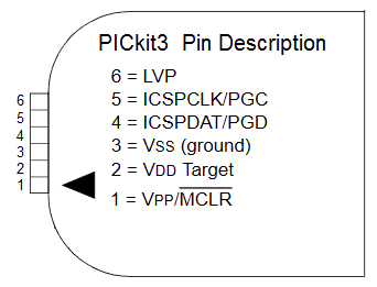
Pinout of the 'PICkit 3' debug / programming adapter
in the author's favoured orientation (DUT on the left).
For dsPIC, leave LVP (Low-Voltage Programming) open.
As so often with MPLAB X, the initial download into the device took ages,
and in this case wasn't even successful:
*****************************************************

Connecting to MPLAB PICkit 3...

Currently loaded firmware on PICkit 3
Firmware Suite Version.....01.55.01 *
Firmware type..............Enhanced Midrange

Now Downloading new Firmware for target device: dsPIC33EP32GS502
Downloading bootloader
Bootloader download complete
Programming download...
Downloading RS...
RS download complete
Programming download...
Downloading AP...
AP download complete
Programming download...

Currently loaded firmware on PICkit 3
Firmware Suite Version.....01.56.07
Firmware type..............dsPIC33E/24E

Target voltage detected
Target Device ID (0x0) is an Invalid Device ID. Please check your connections to the Target Device.
A full-text search revealed this (in the GPSDO sourcecode):
// 2016-04-13: Tried to program a dsPIC33EP32GS202 with PICkit 3, but all
//             it said (on the first attempt) was
//     " Target Device ID (0x0) does not match expected Device ID (0x6d110000). " .
//             WTF ? ?  From a forum:
//      > The message ""Target Device ID (0x0) does not match expected Device ID (0x27e0)",
//      > simply means the programmer is not communicating with the device at all.
//             Heavens no. "Cannot communicate with target device" would be
//             what less brain-amputated IDEs would say in such a case.
//             The problem was caused by a missing 'Vcap' capacitor for the
//             1.8 Volt 'core' supply. Tried again, and got the next error:
//    " Programming/Verify complete.
//      The target device is not ready for debugging. Please check your
//      configuration bit settings and program the device before proceeding.
//      The most common causes for this failure are oscillator and/or PGC/PGD settings. "
//      Indeed, fixed by replacing "#pragma config ICS = PGD1" with PGD3 .
//      After that, successfully started a debugger session but always ended
//      in line " while( OSCCONbits.COSC != 0b011 ); " . More details there....
After adding multiple ceramic caps very close to the "VCAP" pin (20) and GND (19)
on the improvised 'evaluation board':
*****************************************************
Connecting to MPLAB PICkit 3...

Currently loaded firmware on PICkit 3
Firmware Suite Version.....01.56.07
Firmware type..............dsPIC33E/24E

Target voltage detected
Target device dsPIC33EP32GS502 found.
Device Revision ID = 4007
DEVSN0 = 00000000
DEVSN1 = 00000000

Device Erased...

Programming...

The following memory area(s) will be programmed:
program memory: start address = 0x0, end address = 0xdff
Programming/Verify complete

Running

Halting...

Target Halted
But now the 3.3 Volt LDO powering the 'breadboard' got quite hot.
Hmm.. where is the debugger's 'disassembly' or 'code memory' display ?
There was "Window".."Debugging".."Disassembly", but that display
did not show the current execution point (even when paused/stopped/"halted").
There was also "Window".."Target Memory Views".."Program Memory",
but also no highlighted line there.
2.8.1 How to program a "standalone" firmware with PICkit 3
After finishing a debug session (with the code running "almost properly" on a dsPIC33E),
the target was powered off, the PICkit 3 disconnected, and the power turned on again.
On most other microcontrollers, one would expect the device to "simply start".
But not so with a dsPIC, because MPLAB X / PICkit 3 had to program a "debug executive"
downloaded into the program memory. That "debug executive" seems to remain there,
and it prevents a normal launch of the application. The PICkit 3 User Guide explained
in an FAQ style:
> I have finished debugging my code. Now I've programmed my part,
> but it won't run. What's wrong ?
Answer:
- Have you selected the debugger as a debugger and then tried
to program a production device? Programming a device when the debugger
is a debugger will program a debug executive into program memory
and set up other device features for debug (see Section 2.6.1
"Sequence of Operations Leading to Debugging").
To program final (release) code, select the debugger as a programmer.
- Have you selected "Release" from the Build Configuration drop-down list
or Project menu?
You must do this for final (release) code. Rebuild your project,
reprogram the device, and try to run your code again.
How to do this in MPLAB X (v5.45) ? As usual, quite counter-intuitive !
Right-click into the "Projects"-tree. There's a menu item named
Make and Program Device
Invoke this. The "PICkit 3" window then showed:
*****************************************************
Connecting to MPLAB PICkit 3...

Currently loaded firmware on PICkit 3
Firmware Suite Version.....01.56.07
Firmware type..............dsPIC33E/24E

Target voltage detected
Target device dsPIC33EP32GS502 found.
Device Revision ID = 4007
DEVSN0 = 00000000
DEVSN1 = 00000000

Device Erased...

Programming...

The following memory area(s) will be programmed:
program memory: start address = 0x0, end address = 0xdff
Programming/Verify complete
Target removed
This seemed to kill the "debugging executive" in Flash,
so there's no need to duplicate the 'default' project configuration
(with debugging enabled) into a 'production' project configuration.
There was no "Release" configuration selectable in the auto-created MPLAB X project at all.
2021-07: In some cases (Si5351A RF Synth with dsPIC33EP64MC502), the above didn't work.
Even after turning off the power, disconnecting PICkit 3, and turning on again,
the PIC didn't start (not even an 'early sign of life' from the target's
red 'debug LED'). WTF is wrong with the mimosa ? To be continued...
- The target voltage appeared 'a bit more stable' and 0.1 V higher
when the PICkit 3 was connected.
- But despite a 1-kOhm pull-up on /MCLR, and the dsPIC programmed with
the 'standalone' application (which occasionally started without problems),
it NEVER started while PICkit 3 was connected.
Nnngrrr... PICkit 3 always pulls /MCLR down.
- Die Funktion 'Disconnect from Debug Tool' (in MPLAB-X) ist völlig zwecklos.
- Beim Wieder-Anwerfen des Debuggers (als im Target 'gar nichts mehr ging')
zeigte der Debugger dann einen in "void _trapISR _StackError(void)"
gefangenen dsPIC, aber das ist eine andere Geschichte.
Somewhere between MPLAB X v5.45 and v5.50, a new menu item appeared under
'Production' ... 'Program Device for Production'. Aaah. Similar as the old
'Make and Program Device' stupidly hidden in the project tree's
context menu, this seems to program the target WITHOUT the "debugging executive",
but still the PICkit 3 had to be disconnected from the target MANUALLY
to let it 'run free'.
2.8.2 PICkit 3 : The never-ending hassle with 'Failed to program device' / 'Connection failed' / etc^10
Every once in a while, MPLAB X (v5.45 at the time of this writing) failed to download
a freshly built application into the target, at the begin of a debugger session.
The developer was often 'surprised' by output like the following, in MLPAB X's
"Output" window on the "PICkit 3" tab:
*****************************************************

Connecting to MPLAB PICkit 3...

Currently loaded firmware on PICkit 3
Firmware Suite Version.....01.56.07
Firmware type..............dsPIC33E/24E

Target voltage detected
Target device dsPIC33EP64MC502 found.
Device Revision ID = 4008

Device Erased...

Programming...

The following memory area(s) will be programmed:
program memory: start address = 0x0, end address = 0x5fff
configuration memory
User Id Memory
Failed to program device
...
The following memory area(s) will be programmed:
program memory: start address = 0x0, end address = 0x5fff
configuration memory
Failed to program device
...
Unable to download debug executive
Unable to download program executive
Failed to program device
The next day:
...
The following memory area(s) will be programmed:
program memory: start address = 0x0, end address = 0x57ff
configuration memory
Programming/Verify complete
The target device is not ready for debugging.
Please check your configuration bit settings
and program the device before proceeding.
The most common causes for this failure are oscillator and/or PGC/PGD settings.
Target removed            (when disconnecting the supply voltage)
Target voltage detected   (after reconnecting the supply voltage)
Target device dsPIC33EP64MC502 found.
Device Revision ID = 4008 (aha, Mr. PICkit and Mr. dsPIC are still with us)
Double-checked the configuration bits, in this case in
C:\pic\dsPIC33EP_Si5351_Synth\dsPIC33EPxx_Drivers\ConfigBits_dsPIC33EPxxxMC502.c :
// FICD ... controls In-Circuit Debugging .
#pragma config ICS = PGD1   // ICD Communication Channel Select bits (Communicate on PGEC1 and PGED1)
#pragma config JTAGEN = OFF // JTAG Enable bit (JTAG is disabled)

// FPOR ... no idea what that's supposed to be. Funny-Power-On-Reset ? Nope. This location controls "ALTI2C" and "WDTWIN".
#pragma config ALTI2C1 = OFF // don't use Alternate I2C1 pins
  // dsPIC33EPxxMC502 "ASCL2" on RB6 (not remappable) ->
#pragma config ALTI2C2 = ON  // use ALTERNATE I2C2 pins !
#pragma config WDTWIN = WIN25 // Watchdog Window Select bits (WDT Window is 25% of WDT period)

// FWDT ...
#pragma config WDTPOST = PS32768 // Watchdog Timer Postscaler bits (1:32,768)
#pragma config WDTPRE = PR128 // Watchdog Timer Prescaler bit (1:128)
#pragma config PLLKEN = ON    // PLL Lock Enable bit (Clock switch to PLL source will wait until the PLL lock signal is valid.)
#pragma config WINDIS = OFF   // Watchdog Timer Window Enable bit (Watchdog Timer in Non-Window mode)
#pragma config FWDTEN = OFF   // Watchdog Timer Enable bit (Watchdog timer enabled/disabled by user software)

// FOSC ...
#pragma config POSCMD = EC    // Primary Oscillator Mode Select bits (EC (External Clock) Mode)
#pragma config OSCIOFNC = ON  // OSC2 Pin Function bit (OSC2 is general purpose digital I/O pin)
#pragma config IOL1WAY = OFF  // Peripheral pin select configuration (Allow multiple reconfigurations)
#pragma config FCKSM = CSECME // Clock Switching Mode : Both Clock switching and Fail-safe Clock Monitor are enabled

// FOSCSEL ...
#pragma config FNOSC = FRC    // Oscillator Source Selection (Internal Fast RC (FRC))
#pragma config PWMLOCK = OFF  // PWM Lock Enable bit (PWM registers may be written without key sequence)
#pragma config IESO = ON      // Two-speed Oscillator Start-up Enable bit (Start up device with FRC, then switch to user-selected oscillator source)
Nothing wrong with that. In the meantime, MPLAB X decided it wanted some stupid updates. Installed them.
After that, MLPAB-X didn't detect PICkit3 anymore ("No Tool"). More on that later.
2.8.3 More 'fun' with MPLAB X : "The target device is not ready for debugging"
Because the 'not ready for debugging' message (repeated a couple of times)
frequently came back to haunt the developer, precious time was wasted to investigate this:
Fatal error: 0xc04
The target device is not ready for debugging. Please check your configuration bit settings and program the device before proceeding. The most common causes for this failure are oscillator and/or PGC/PGD settings.
The target device is not ready for debugging. Please check your configuration bit settings and program the device before proceeding. The most common causes for this failure are oscillator and/or PGC/PGD settings.
The target device is not ready for debugging. Please check your configuration bit settings and program the device before proceeding. The most common causes for this failure are oscillator and/or PGC/PGD settings.
The target device is not ready for debugging. Please check your configuration bit settings and program the device before proceeding. The most common causes for this failure are oscillator and/or PGC/PGD settings.
The target device is not ready for debugging. Please check your configuration bit settings and program the device before proceeding. The most common causes for this failure are oscillator and/or PGC/PGD settings.
The target device is not ready for debugging. Please check your configuration bit settings and program the device before proceeding. The most common causes for this failure are oscillator and/or PGC/PGD settings.
.. etc etc, stupidly repeated all over again, as if we hadn't seen it yet..
But the confusing menu ("Production") has this never-used-before item
"Program Device for Debugging" .. maybe this is more successful ?
But then... surprise surprise, even more 'fun' from MPLAB X:
Launching
Programming target
Failed to program the target device
The debugger could not be started.  Terminating debug session.
User program finished
"Program Device for Debugging"
Surprise surprise, despite having successfully built (compiled, linked) the
application, this time the stupid IDE pops up with a modal error message box:
      Error
C:/Faselblah/somewhere.X/dist/default/debug/ProjectName.X.debug.elf
does not exist or is not an executable.
Being fed up with this piece of crap, the author decided to terminate
MPLAB X, clear all that junk in "dist/default/debug" (just in case..)
but there was no *.elf anywhere in this ".X/dist/default/debug"-crap,
only in ".X/dist/default/production". It appears that the menu item
"Program Device for Debugging"
is useless because there's no way to generate the *.elf for *DEBUGGING* -
at least not in under 'Production' menu, where all these items were located.
To make a long and nerve-wrecking story short:
TERMINATE MPLAB X.
Disconnect PICkit (3 or 4) from USB.
Disconnect PICkit (3 or 4) from target.
Disconnect supply voltage from target.
Shutdown and reboot the (Windows)-PC. (yes, this was NECESSARY, more than once)
Reconnect PICkit (3 or 4) to USB and target.
Reconnect external supply voltage to target.
Restart MPLAB X and go the kitchen to have a cup of coffee.
Return to the shack; maybe MPLAB X has already loaded the project.
Click "Debug".."Debug Project".
This time:
The target device is not ready for debugging. Please check your configuration bit settings and program the device before proceeding. The most common causes for this failure are oscillator and/or PGC/PGD settings.

   (but..)

*****************************************************

Calculating memory ranges for operation...

Erasing...

The following memory area(s) will be programmed:
program memory: start address = 0x0, end address = 0x97ff
configuration memory

Programming/Verify complete

Running
Target Halted
Oh well - forgot to remove the old breakpoints, which MPLAB X seems to remember
in some black hole in their ".X"-thingy (project folder).
So kill all breakpoints, click the blue-disk-with-two-funny-white-arrows-RESET-icon
- et voila, the Mimosa is willing to debug again, because the green arrow
now points to the first executable statement in our 'main()' function again.
We'll possibly never find the reason for
target device is not ready for debugging
(it's not the configuration memory), but anyway.
Keep this chapter for the the future; this bug returned many times.
2025-11-10: Indeed, the trouble with "The target device is not ready for debugging"
returned, this time after successfully programming a PIC18F25J50 (one of the
rare PICs with homebrew friendly standard DIL package and built-in USB controller):
Script GetVersionDE failed with status Type = runScript,
Script name = GetVersionDE, Status = 0xa00.
The target device is not ready for debugging. Please check
your configuration bit settings and program the device before proceeding.
The most common causes for this failure are oscillator and/or PGC/PGD settings.
To check the homebrew 'eval board' and the debugger connection (PICkit4),
selected "Production" .. "Clean and Build Project" + "Program Device for Production".
Result (on a tab labelled "PICkit 4-usbcdcdemo"):
Connecting to MPLAB PICkit 4

Currently loaded versions:
Application version...........02.01.35
Boot version..................01.00.00
PCB version...................4
Script version................00.06.71
Script build number...........74cdf38a4d
Tool pack version ............2.3.1848
Target voltage detected
Target device PIC18F25J50 found.
Device Revision Id  = 0x4
Device Id = 0x4c20

Calculating memory ranges for operation...

Erasing...

The following memory area(s) will be programmed:
program memory: start address = 0x0, end address = 0x3ff
program memory: start address = 0x1000, end address = 0x27ff
configuration memory

Programming/Verify complete
Double-checked what the "usbcdcdemo" had in the project's "sysconfig.h" (a file that was
formerly called "fuses.h", with dozens of "#pragma config" instructions for "XC8").
The reason for being able to PROGRAM the PIC18F, but not to DEBUG anything,
was a wrong OSCILLATOR configuration. Remember: Unlike modern CPUs, to DEBUG on an
8- or 16-bit PIC (including dsPIC), the IDE (MPLAB-X) must load a hidden "debugging
executive" into the target, running before the APPLICATION FIRMWARE (?), and that
seens to be affected by wrong settings in the FUSE BITS aka "Configuration Memory".
This is VERY different from e.g. ARM / Cortex, where the debugger can run EXACTLY THE SAME
FIRMWARE that will be used for "Production" later. Not so with a PIC.
New "nice suprises" in March 2024: Debugger-troube a go-go again..
The configuration is set for the target board to supply its own power but no voltage has been detected on VDD. Please ensure you have your target powered up and try again.
Connection Failed.
  (that happened with an original 'PICkit4', not one of the crappy-junk-from-you-know-where fake "clone".
   Voltages at the PICkit4's "GND" (pin 3) and "VCC" (pin 2, +3.3 Volts in this case) were ok.
   The same crap with a target board that had been successfully used a few months ago.
   The reason was, as often, not the target board but the incredibly bugged IDE,
   or unstable communication between the bugged IDE and the debugger itself.)
Transmission on endpoint 2 failed (err = -10022)
You have set the program speed to Normal. The circuit on your board may require you to slow the speed down. Please change the setting in the tool properties to low and try the operation again.

Failed to get Device ID. Please make sure the target device is attached and try the operation again.
Connection Failed.
Transmission on endpoint 2 failed (err = -10022)

Launching
Could not acquire hardware tool communications resources: pk4hybrid SN#BUR210572199
The debugger could not be started.  Terminating debug session.
User program finished
> Stability improvements in USB tool interface connectivity .
"Stability improvements" ? Sounds great - MPLAB X was in dire need of hundreds of such improvements,
so the frustrated author gave "Version 6.20" a try.
More about the migration from MPLAB X Version 5.50 to Version 6.20 is in another chapter
Again, after MPLAB X decided to install some crappy update (and the developer was
stupid enough to click on the stupid bubble to install the stupid update),
MLPAB-X didn't detect the PICkit3 anymore ("No Tool").
Only the trusty old MPLAB 8.92 was still happy with the same USB port, same PICkit 3,
same target board:
PICkit 3 detected
Connecting to PICkit 3...
Running self test...
Self test completed
Firmware Suite Version...... 01.56.07
Firmware type......................dsPIC33E/PIC24E
PICkit 3 Connected.
Target Detected
Device ID Revision = 00004008
Deleted MPLAB-X, including ALL versions, including ALL of its 'Persistent Folders'
(whatever that means), leaving only MPLAB 8.92 and the XC16 toolchain installed.
To give the piece of junk (MPLAB X) another chance, downloaded
"MPLABX-v5.50(1)-windows-installer.exe", which surprisingly recognized
PICkit 3 again (and listed it again in the 'Project Properties' tree).
Even the message "The target device is not ready for debugging"
disappeared after doing the 'complete, clean re-install'. Phew. Only one working day wasted.
Lesson to be learned: DON'T LET MPLAB-X UPDATE ANYTHING YOU DON'T USE,
DON'T INSTALL 'DEVICE PACKS' (unless you really need them),
DON'T LET MPLAB-X DESTROY A SUFFICIENTLY FUNCTIONAL INSTALLATION !
If it's not broken, don't fix it. If you fix it, it will break.
Or, as someone wrote in a forum:
MPLab X (..) just pupped up a bubble prompting me to install an updated XYZ plugin.

Like an idiot, I clicked on the bubble and the update tried to install.
But then it died.
A few of other 'nice surprises' from MPLAB X and/or PICkit 3:
This is 'almost normal'. Disconnect PICkit 3 from target (not from USB). Wait. Reconnect.
The PICkit's "STATUS" LED should be mostly GREEN, and only occasionally flash up in RED.
Try again, et voila (in most cases):
Connecting to .. blah, blah..
Target voltage detected (would be nice if they already told us THE VOLTAGE)..
Target device XYZ found. ...
Device Erased...

Programming...  .... .....
Programming/Verify complete

Running
Target Halted
2.8.5 MPLAB-X, PICkit 4, and a dsPIC33EP64MC502 : Sluggish response during a debug session"
Ok, so I finally bought a PICkit 4 after discovering at the office
that programming, and (under certain circumstances) single-step debugging
with a PICkit 4 is usually faster than with a PICkit 3.
But then (in the meantime, with MPLAB X v5.50), strange things happened.
Difficult to say if the bloated Java/Netbeans monster is to be blamed,
or the PICkit.
Scenario: The target is running during a debugger session.
We already know that MPLAB-X and PICkit (3 or 4) are unable
to set a new breakpoint while the target is running. Oh well.
So klick on the "Pause"-button, wait patiently until the debugger
does what we ask it for, but ... NOTHING HAPPENS. The goddamned
'Pause' button in MPLAB X simply stays enabled (as if we didn't
click it at all).
The target just keept running. Then, a long time later:
Running

Halting...

An internal run error has occurred. (AH, WOULDN'T BE THE FIRST.)
It is advised that you restart your debug session.
You may continue running but certain run time features
may no longer work properly.

Target Halted
Nnngrrrr. Terminated the debug session, to try again as 'advised'.
This time, PICkit 4 was able to pause the target within a few seconds.
Hmmm... this was never a problem with the old PICkit 3 ?!
At the office (where, at the time of this writing the author was developing
a 'low-power application' for a PIC16F18325), similar problems
with an 'unstoppable target' seemed to be related with the PIC's
current clock source: When clocked from the internal 31 kHz oscillator,
a click on the debugger's "Pause"-button also took ages until
the target really stopped (could be easily be seen by a flashing
'debug LED').
Out of the blue, another 'surprise' from the bloated IDE (MPLAB X):
Error: Project "dsPIC33_Si5351_Synth" refers to file "p33EP64MC502.h" which does not exist in the disk. The project failed to load.
<dontknowwhere><dontknowwhy>/packs/Microchip/dsPIC33E-yaddayadda../xc16/support/dsPIC33E/h
which SHOULD have been
<somewhereelse><whattheheck>/packs/Microchip/dsPIC33E-blah_blubb../xc16/support/dsPIC33E/h
To avoid dependencies from those ever-changing paths to include directories,
the author decided to copy the required files from the 'support' folder
to a project-specific folder itself, so when zipping the project-specific folder,
all "required" include files that once were in a 'pack' would be in there.
In this case, there was already a folder with CPU-specific includes
(C:\pic\dsPIC33EP_Si5351_Synth\dsPIC33EPxx_Drivers), so that
was where the following header files (that MPLAB X was 'suddenly' unable to find)
where copied, and manually added to the project tree under 'Header Files':
p33EP64MC502.h p33EP512MC502.h (two machine-generated monsters with almost the same content).
Years later (anno 2026), MPLAB-X still appears to be an unreliable mimosa. When debugging code in a PIC16F1847 using PICkit4,
debugging first started, but after a few click on "Pause" and "Run", all buttons to control the target
were grayed out, and the MPLAB-X showed this in the "Output" window:
Halting...
Time out waiting for tool lock

Unable to run the target device.
The tool was disconnected while it was busy.
A "debug LED" driven via GPIO, toggled in every main loop, confirmed the target (PIC16F1847)
was still alive and running. But MPLAB-X / PICkit4 was unable to stop ("pause") it. After
clicking the "Pause" button, all debugger controlbuttons except "Finish Debugger Session"
were grayed out, but even "Finish Debugger Session" didn't do anything.
When terminating the bulky sluggish IDE, it complained (as usual) about
"this will terminate blah, blah, blah...", so "Exit IDE" had to be clicked several times
until the stupid IDE really terminated itself.
After disconnecting / reconnecting PICkit4 from USB, starting MPLAB-X again, and waiting patiently for some bizarre "background activities"
to finish, a new debug session could be launched. History repeating.. see chapter
More 'fun' with MPLAB X : "The target is not ready for debugging"
Asked an AI for a possible reason, and got this response:
The primary reason for this error is a sudden breakdown in hardware communication
or a locked software process between MPLAB X, your computer's
USB controller, and the hardware tool (such as a PICkit, ICD, or Snap)
while it was actively processing a command.
Hardware & Power Causes
- USB Power Drop: The target board or hardware tool
drew too much current, causing the voltage rail
to dip and forcing the tool to brown out or reset
mid-operation.
- Loose Connections: The USB cable, ICSP cable, or
target board power cable became physically loose
or disconnected.
- Target Board Power Loss: The target device lost
external power, or MPLAB X is not configured to supply
power from the tool when external power is missing.
( sounds logical, but none of the above guesses by the AI was the reason)
Software & Firmware Causes
- Crashed Background Process: A background Java thread
or hardware tool driver in MPLAB X froze,
locking up the communication pipeline ("Tool Lock").
- Corrupted IDE Cache: A known issue in certain MPLAB X
versions causes project configurations to freeze up
inside the workspace cache directory.
The author decided to not waste more time on this.
Lesson to be learned:
- If the "Pause" button for the debugger doesn't react
within say ten seconds,
pull out the USB cable between PC and PICkit4.
This often (but not always) lets the stupid Java thread
(most likely the one that chews on the USB communication) die,
so you can to launch another debugger session
without having to exit and restart the crazy IDE.
2.9 Migration from MPLAB X Version 5.50 to Version 6.20
Like an old Windows installation which gradually destroys itself after too many "updates"
(until the point where it gets too slow to be useful, and boots like an IBM PC AT trying
to load Windows 3.0), it was time to pull the plug completely,
and get rid of the crap that the old MPLAB X had deposited in the Windows registry and on the
disk. The uninstaller for MPLAB X Version 5.50 took almost as long as downloading
the 880 MByte monster-installer for MPLAB X Version 6.20. For a start (and this may
turn out to be a mistake later), the various C compilers and stoneage assemblers for the
old PICs (which by the way had a completely different syntax than the "new" assembler for
PIC12 / PIC16 / PIC18) were kept untouched, hoping that the updated MPLAB X would recognize
them as "tool locations" (or whatever they call it).
Some ghost of the crashed (and, at that time, already uninstalled) MPLAB X V5.50
was still haunting the system, and cause the installer for Version 6.20 to complain
Please close all instances of MPLAB X before running this installer.
Oh well, time for a complete system re-boot. Time for a tea. Wait for windows to start.
Wait for the installer to start. Remember NOT to install MPLAB X where Microchip wants us
to install each and everything .. here:
"Installation Directory" not "C:\Program Files\Microchip\MPLABX\v6.20"
but
"C:\tools\Microchip\MPLABX"
(note the lack of a VERSION SUBDIRECTORY; having ONE intallation of this bulk is enough)
Also uncheck
[ ] I consent to allow the collection of .. info ..
(heavens no, MPLAB X is already slow enough doing the things we EXPECT it to..)
[ ] I would like to enable Product Change Notifications through MPLAB X ...
(NO, I DON'T. A "C" development IDE shall not act like a bugged web browser.)
"Chose which Microchip device support you want to install:"
[*] 8-bit MCUs (2.5 GByte)
[*] dsPIC DSCs and 16-bit MCUs (2.7 GByte)
[ ] 32-bit MCUs and MPUs (3.7 GByte) [heavens no, use Keil's blazingly fast uVision and ARM/Cortex]
[ ] Other devices [no thanks, not with a Java-based tranquilized snail like MPLAB X]
About half an hour later, the installer asked about which COMPILER(S) to install,
offering the following choices:
[*] Install latest MPLAB XC8 compiler v2.46 (8-bit devices)
[*] Install latest MPLAB XC-DSC compiler v3.00 (dsPIC DSC devices)
[*] Install latest MPLAB XC16 compiler v2.10 (16-bit PIC24 devices)
[ ] Install latest MPLAB XC32 compiler v4.35 (32-bit devices)
Surprise surprise. Did they really DROP SUPPORT for dsPIC33 in XC16 ?
Anyway, install the flasy new "XC-DSC" (whatever a "dsPIC DSC" may be - a "new kind of dsPIC" ?) besides XC8 and XC16.
Previously (with MPLAB X V5.x), all dsPIC33
-> "Connecting to remote server" .. "Downloading" ... ... ...
And again, don't install the compilers where MICROSOFT wants us to install anything.
In this case, XC8 was installed into THE SAME FOLDER IN WHICH IT HAS ALWAYS BEEN:
"C:\tools\Microchip\xc8v2" .
Similar (NOT in "C:\Program Files\blabla") for other Microchip C compilers:
"XC-DSC" (which didn't exist in older installations) was installed into..
"C:\tools\Microchip\XC-DSC" .
(again, note the lack of any VERSION-DEPENDENT STUFF in the whole path; having ONE intallation of XC16 is enough)
Some speculations about "XC-DSC" versus "XC16", from a forum:
> IMHO You should move to XC-DSC whenever possible, if your project targets a dsPIC.
> The compiled code output is more or less the same (there are differences that i
> can't see in the listing file, should be something in the standard c library,
> but all of my code generate the same output), however the internal version of GCC
> is 8.3.1 instead of being GCC 4. The warning system is much more advanced.
> Besides, it's hinted that XC16 will gradually drop dsPIC support over time.
> Don't mind the bogus warning about a missing license, it's bogus.
Finally, XC16 was installed into WHERE IT HAS ALWAYS BEEN :
"C:\tools\Microchip\xc8v2" .
(and again, the lack of any VERSION-DEPENDENT STUFF in the whole path; having ONE intallation of XC16 is enough)
On the first launch of the shiny new "MPLAB X Version 6.20", it imported some
"settings" (whatever that means) and "window positions" from v5.50.
Then, it took endlessly to start (as any MPLAB X before).
Then, after finally loading the project (-folder) created by the old IDE,
V6.20 complained:
+ Configuration "default" load error: dsPIC33E-GM-GP-MC-GU-MU_DFP 1.3.85 is used in the configuration and it is not installed
Resolution: Click on the below link to resolve the same version of DFP
Resolve DFP for configuration: default
In the project ("Bat_Converter" with dsPIC33EP512MC502), selected the only-available
"Packs: dsPIC33E-GM-GP-MC-GU-MU_DFP 1.5.258".
The "XC16 (v1.70)" indicated in the "Project Properties" was plain wrong,
the compiler actually invoked the freshly installed XC16 V2.10.
Next: Try to "build all" (aka "Production" .. "Clean and Build").
Result:
make  -f nbproject/Makefile-default.mk dist/default/production/Bat_Converter.X.production.hex
elf-gcc.exe: warning: -legacy-libc is deprecated
elf-gcc.exe: warning: -legacy-libc is deprecated
elf-gcc.exe: warning: -legacy-libc is deprecated
elf-gcc.exe: warning: -legacy-libc is deprecated
elf-gcc.exe: warning: -legacy-libc is deprecated
Emitting the same warning over and over again doesn't help - WHICH MODULE (or even
Microchip's own library modules) causes these problems ? Not solved yet.
At least, similar to an older MPLAB-X-update, this update made the
PICkit4 do its job again (possibly caused by the IDE performing a FIRMWARE UPDATE
for the PICkit without asking for permission.. anyway, the PICkit4 surived,
and the debugger trouble listed here
vanished here - at least for the end of the day, and until the debugger
died again during a successfully started debug-session.
3. Fairly new PIC projects by DL4YHF (beginning 2021)
3.1 Improvised 'evaluation board' for dsPIC33EP32GS502
For new PIC projects, a bunch of dsPIC33EP32GS502-I/SO was ordered from Mouser
in 03/2021 (3.16 Euro per chip, w/o tax). One of the five chips was soldered to a
simple hand-milled, copper-clad "evaluation board":
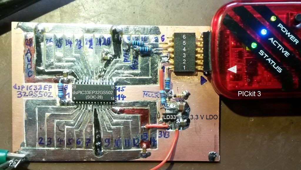
DL4YHF's improvised homebrew dsPIC33EP32GS502 "evaluation board"
with only the vital components populated. Click for full-size image.
Some time later, the "eval board" was populated with a cheap 1.8" TFT,
a rotary encoder with pushbutton, and an RGB indicator LED (multiplexed
with the pushbutton/encoder signals):
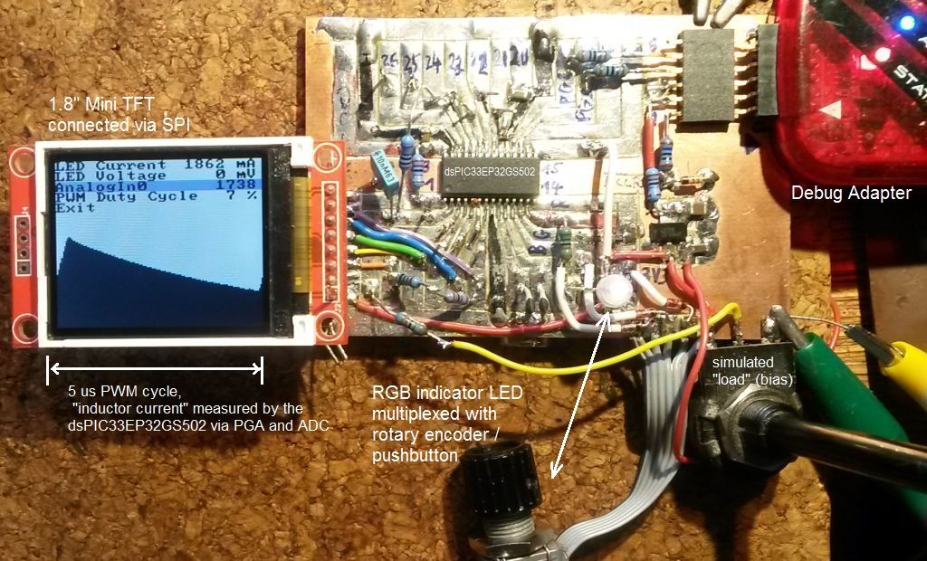
dsPIC33EP32GS502 'eval board' with "graphic user interface" :o)
4. Locally saved PIC datasheets and appnotes
Links in this html document are "local", into the folder with datasheets,
application notes, programming references, etc, all in PDF format,
rescued from the Microchip website (because no link to their website
would work for more than a few years, since they keep moving their files around).
At the time of this writing, the local "PIC datasheet" folder was c:\datasheets\pic .
AN0617.pdf : "Fixed Point Routines" (Multiplication and Division on PIC16 and PIC17)
dsPIC30F2010.pdf
dsPIC30F3013_datasheet.pdf
dsPIC30F_to_dsPIC33FJ16GSX_Migration_4MSps_SPDIP28.pdf
dsPIC30_Flash_Prog_70102e.pdf
dsPIC30_vs_dsPIC33.pdf
dsPIC33EP256GP502_Errata.pdf
dsPIC33EP256GP502_SPDIP28_12bit_500kSps_ADC_Digikey.pdf
dsPIC33EPxxGS202_Errata.pdf
dsPIC33EPxxGS202_Family_with_12bit_3MSps_ADC.pdf
dsPIC33EPXXGS202_Flash_Memory_Programming.pdf
dsPIC33EPxxGS502_Family_with_12bit_3MSps_ADC.pdf (DS70005127D, anno 2015)
dsPIC33EP16/32/64GS502 (DS70005127D, anno 2017)
dsPIC33EPXXGS50X-Family-Silicon-Errata-and-Data-Sheet-Clarification-DS80000656J.pdf READ THIS CAREFULLY - especially for early chip revisions !!!
dsPIC33EPxxxGP50x.pdf
dsPIC33EVxxxGM_5V_70MIPS_Family_12bit_500kSps_ADC.pdf
dsPIC33E_12-Bit_High-Speed_Multiple_SAR_ADC_DS70005213G.pdf
dsPIC33E_CPU__DS70005158a.pdf
dsPIC33E_Family_Reference_Interrupts_DS70000600E.pdf : Family Reference Manual : Interrupts (anno 2019)
dsPIC33E_Family_Reference__1MSps_ADC_DS70621C.pdf
dsPIC33E_Family_Reference__CPU_DS70359B.pdf : "Section 2 : CPU" (Section 2 of yet another 'Family Reference Manual', anno 2010)
dsPIC33E_CPU_DS70000157G.pdf : "Family Reference Manual : CPU" (mainly the instruction set, anno 2018)
dsPIC33E_Family_Reference__Interrupts__DS70000600d.pdf
dsPIC33E_HighSpeedPWM_DS70645C.pdf
dsPIC33E_HighSpeedComp_DS70005128.pdf ("High-Speed Analog Comparator Module" especially for dsPIC33E, certain "GS" devices)
dsPIC33E_Output_Compare__DS70000358C.pdf
dsPIC33E_UART_DS70000582e.pdf
dsPIC33FJ128GP802_SDIP28_40MIPS_2x16bitDAC_12bit_500kSps_ADC.pdf
dsPIC33FJ12MC201_202_DIL28.pdf
dsPIC33FJ16GSX02_10bit_4Msps_ADC_SPDIP28.pdf
dsPIC33FJxxGSxxx_High_Speed_Analog_Comparator_DS70296C.pdf
dsPIC33EPxxGS502_High_Speed_Analog_Comparator_DS70296C.pdf
dsPIC33_Family_Oscillator_DS70005131a.pdf
dsPIC33E_HighSpeedPWM_DS70000323H.pdf
dsPIC33_Input_Capture__DS70000352C.pdf
dsPIC33_SMPS_FAQ_with_Code_Examples_DS93062A.pdf
dsPIC33_Timers_DS70362.pdf
dsPIC_Oscillator_Config_70054e.pdf
dsPIC_Quick_Reference_Guide.pdf
pic12f675_datasheets.pdf
PIC16F1716_SDIP28_ohne_EEPROM.pdf
PIC16F1847_PDIP18_pincompatible_with_PIC16F628A.pdf
PIC16F1782_3_datasheet.pdf
PIC16F1782_Errata.pdf
PIC16F1783_PWM_Appnote.pdf
PIC16F1786_SDIP28_2Euro50_Reichelt_2015.pdf
pic16f1788_datasheet.pdf
PIC16F178x_Flash_Prog_41457E.pdf
PIC16F1xxx_HEF_Self_Programming_AN1673.pdf
PIC16F628A_datasheet.pdf
pic16f628_datasheet.pdf
pic16f688_datasheet.pdf
PIC16F688_prog_spec.pdf
pic16f690_datasheet.pdf
pic16f690_prog_spec.pdf
pic16f76_datasheet.pdf
pic16f84a_datasheet.pdf
pic16f87x-flash-programming.pdf
pic16f87x_datasheet.pdf
PIC16F882_3_4_5_6_7.pdf
PIC18F24J50_PIC18F25J50_PIC18F26J50_PIC18F44J50_PIC18F45J50_PIC18F46J50_SDIP28_25mA_kein_EEPROM.pdf
pic18fxxxx_prog_spec.pdf
PIC32MX150F128B_I_SP_SDIP_28_MCP.pdf
PIC32MX150F128B_SPDIP28_Reichelt_10bit_1MSps_ADC.pdf
PICkit3_PIC16F628_Programming_Adapter.pdf
PICkit3_User_Guide.pdf
PIC_14bit_instruction_set.pdf
PIC_Mid_Range_Manual_DS33023a.pdf
XC16_dsPIC_C_Compiler_Users_Guide_DS50002071.pdf