 |
|||||
|
APPLICATION
|
|||||
 |
|||||
AD9887 Application Note and Function Enhancement
 |
|
The LCD panel needs the DE signal to determine two things. First, the exact start line number after the V-sync signal and end line number of a frame. And, second, the exact start point after the H-sync signal and end point of each horizontal line. The line number between the start line and the end line should be exact 768 (for a 1024X768 panel) or 1024 (for a 1280X1024 panel). The pixel number between the start point and the end point should be exactly 1024 points (for a 1024X768 panel) or 1280 (for a 1280X1024 panel). In order to get stable display, the DE signal should be disabled within the V-sync period.
This is the AD9887 interface timing in VGA mode:
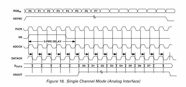
So the DE signal can be composed of the V-sync, H-sync and the pixel clock. Since there are different standards of display mode (for example, VGA, SVGA or XGA) that has different sync polarity and horizontal timing, the pixel counter should be programmable.
For design simplicity and easy operation, the programmable registers should be as less as possible.
|
Register Define |
||
|
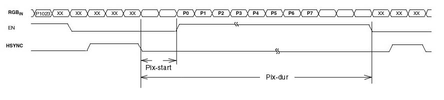
Pix-Start
|
10bit
|
The
clock number between the end of H-sync signal and the start of effective
pixel
|
|
Pix-dur
|
12bit
|
The
effective pixel number within a horizontal line
|
|
Line-Start
|
10bit
|
The
line number between the end of V-sync signal and the start of effective
horizontal line
|
|
Line-dur
|
12bit
|
The
effective line number within a display frame
|
|
H-POL
|
1bit
|
The
polarity of H-sync signal
|
|
V-POL
|
1bit
|
The
polarity of V-sync signal
|
In our
prototype, we use dedicated Pix-start, Pix-dur, Line-start and Line-dur
setting. But if this circuit is embedded into the AD9887 IC, it's better
that these four registers should all be programmable.
We describe our design below:
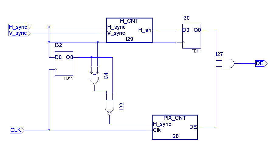
We derive the DE signal in VGA mode from the V-sync, H-sync and Pixel-clock. The H_cnt module is a 10bit counter and two comparator. The two comparators determines from which line the DE should be active, and from which line DE should not be active.
;****** Verilog module *********
module H_cnt(H_sync,V_sync,H_en);
output
H_en;
input H_sync;
input V_sync;
reg [9:0] Q;
assign H_en = ((Q > 10'h1a) & (Q < 10'h31b))? 1 : 0 ;
always@(posedge
H_sync or negedge V_sync)
if(~V_sync)
Q <= 10'b00_0000_0000;
else
Q <= Q + 1;
Endmodule
;******** Verilog module *******
module Pix_cnt(H_sync,Clk,DE);
output
DE;
input H_sync;
input Clk;
reg [9:0] Q;
assign DE = ((Q > 10'h94) & (Q < 10'h295))? 1 : 0 ;
always@(posedge
Clk or negedge H_sync)
if(~H_sync)
Q <= 10'b00_0000_0000;
else
Q <= Q + 1;
endmodule
Despite of the driver circuit, the LCD panel itself is also an important issue. As you have a surplus panel on hand, you need to find the detail specification for it. You can find the datasheet for most recent models. But if you got an antique model, then at least you need to know the follow issues:
A: It uses LVDS interface or parallel CMOS interface?
B: It uses 3.3V or 5V power supply?
C: It works in dual pixel mode or single pixel mode?
D: The power supply range for the backlight inverter.
In this design, I use a HITACHI panel with 3.3V power supply, dual pixel LVDS interface, 12V for the backlight inverter. OK, let's begin.
There are several key issues need to be emphasized,
First, the Vertical sync (V_sync) polarity and horizontal polarity (H_sync) in different display mode. The LCD panel accepts only one dedicated V_sync and H_sync mode, but the V_sync and H_sync have different polarity in VGA, SVGA, XGA and SXGA mode. We need to detect these display modes and convert the V_sync and H_sync into uniform polarity. The mode detection is fulfilled with a AT89C2051 CPU. The CPU also initializes the AD9887 on power up. Also, the CPU needs to select the correct VCO and PLL multiplication number according to the display mode.
Second, the clamping position, please reference the AD9887 datasheet for detail information.
Third, the DE singal generation. We described this issue at the beginning of this page.
Forth, The sampling point for each pixel. The signal bandwidth of the display system is limited typically within 60MHz to 120MHz. It's combination of graphic card, display cable and quantization amplifier. The band limit signal has a relatively long transition time, ether the rising edge or the falling edge. If the sampling is made within the transition time, the quantized display will be blurred, not crisp. So we need to adjust the sampling position to the stable area of the video signal to get optimized contrast. There is a regsiter to adjust the sampling phase in 32 step, that quite enough.
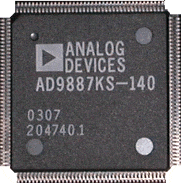
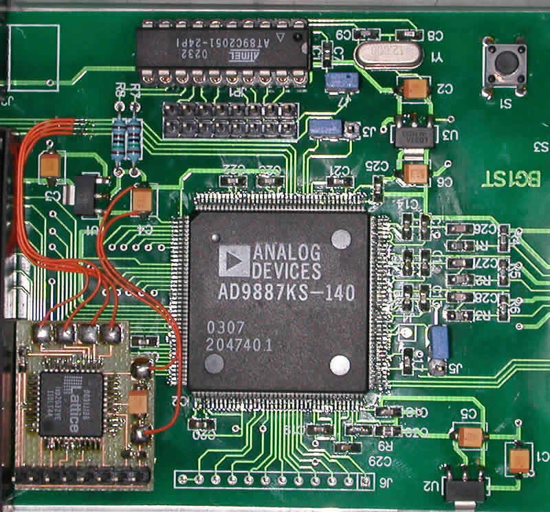
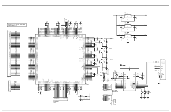
OK, let's take a look of the main board. The main board consists of the AD9887 and AT89C2051 and some regulators. As described above, the AD9887 quantizes the input analog RGB video signal into 8bit digital signal. The RGB signals aredigitized into 8bit, so the panel is capable of 24bit color. The AT89C2051 do three major things: 1: Initial the AD9887's working registers. 2: Detect the current display mode. 3: Provide user interface for fine adjustment of display contrast.
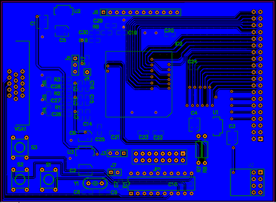
Click the figure for the PDF version:
The display mode is detected automatically by the CPU. When you start your computer, the display mode is 720X400, that's commonly called the DOS mode. If you use MS windows, there are lots of supported modes including :
| VGA | 640X480 | WUGA | 1920X1200 |
| SVGA | 800X600 | QXGA | 2048X1536 |
| XGA | 1024X768 | QUGA | 3840X2400 |
| SXGA | 1280X960 | ||
| WSXGA | 1400X1050 | ||
| UGA | 1600X1200 |
But most surplus parts we can get are within the range of SVGA to UGA, and the AD9887A-170 supports all of these resolutions. For a UGA display, the bandwidth is at least 120MHz, so care must be taken in PCB artwork design to minimize ring and reflection.
Let's take a look of the power supply:
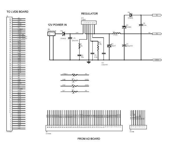
The power supply board consistsof a switching regulator providing 5.0V and 3.3V power for the panel. And an adaptor socket for connection of the LVDC board.
Then take a look of the LVDS board:
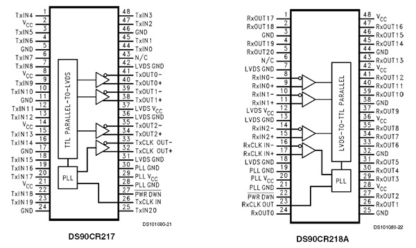
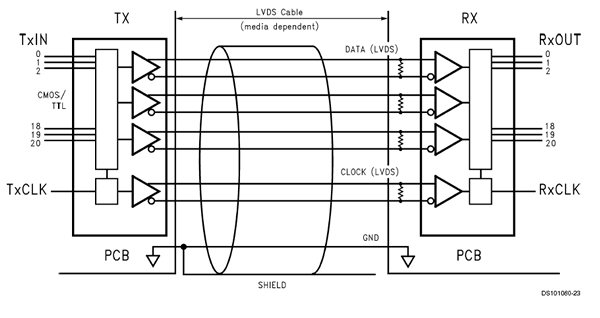
The panel uses dual pixel interface, which means two pixel RGB data are transferred during one clock period. So we need two chips of LVDS transmitter. Because there are too many wires for the parallel data signals, I use a high density PCMCIA socket for the interconnection between the LVDS board and the main board. In fact, it's more convenient to combine the LVDS board and the main board into one PCB.
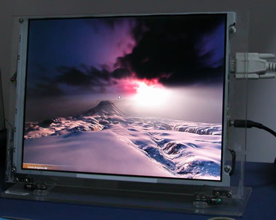
OK, let's have a look of the whole system when completely assembled:
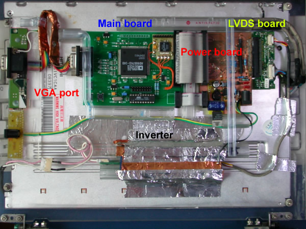


We use this design in a table top LCD pannel.
The LCD is a HITACHI 14.1-inch TFT with 18bit X 2 LVDS interface.
The LVDS tranceiver IC we use is DS90C561.
We get perfect performance in high clock stability, high display contrast, accurate chroma balance and fast response speed.