REVERSE DDS for LOCKED OSCILLATORS |
Reverse DDS use the DDS chip as high speed divider. The output signal is compared with a stable signal (reference). Phase detector output is used to close the loop and to correct the frequency/phase error.
The RDDS is loaded with Hex numbers from the PIC IC to convert the input OCXO clock to the PLL reference frequency. RDDS board can control up to 16 frequencies. Each frequency can be programmed using serial PC Hyperteminal.
It can lock crystal oscillator up to 180MHz (AD9850 tested, overclocked up to 240MHz but is very hot). AD9851 is a better choice.
RDDS support a wide frequency range for reference oscillator: 5 - 20MHz / 300mVpp. I used an VTCXO Motorola 16,8MHz from UHF HT600 radio. For UHF/SHF, the reference source must have a very good stabillity. Excellent is a GPS disciplined oscillator or OCXO.
Controlled oscillator VCXO has Kv 100-125Hz/V (sensitivity of varicap circuit). Initial frequency error must to be < 500Hz, otherwise the PLL can't lock. Coarse adjust the oscillator until PLL voltage control stabilises at about 3-5V for lock condition.
Now the stabillity frequency of my 2m transverter is very good: max. +/- 5Hz in a wide temperature range. Reverse DDS have a low phase noise, more better than a multiplied DDS signal.
For other info please read G4NNS WEB SITE
About Reverse DDS (dead links 16.09.2018)
![]() G4JNT Reverse DDS (G4NNS WEB)
G4JNT Reverse DDS (G4NNS WEB)
![]() HEX CODE PIC16F628 (LINK)
HEX CODE PIC16F628 (LINK)
![]() Schematic RDDS Module (LINK)
Schematic RDDS Module (LINK)
![]() Frequency Word Calculator (LINK)
Frequency Word Calculator (LINK)
![]() G4JNT Old Article (LINK)
G4JNT Old Article (LINK)
![]() RDDS Frequently Asked Questions (LINK) - Read!
RDDS Frequently Asked Questions (LINK) - Read!
![]()
![]() PCB Top
PCB Top
![]() PCB Bottom
PCB Bottom
![]() PCB Components >1< and >2< (are not 1:1 scale)
PCB Components >1< and >2< (are not 1:1 scale)
![]() BLOCK DIAGRAM yo4hfu
BLOCK DIAGRAM yo4hfu
![]() Reference Oscillator - schematic
Reference Oscillator - schematic
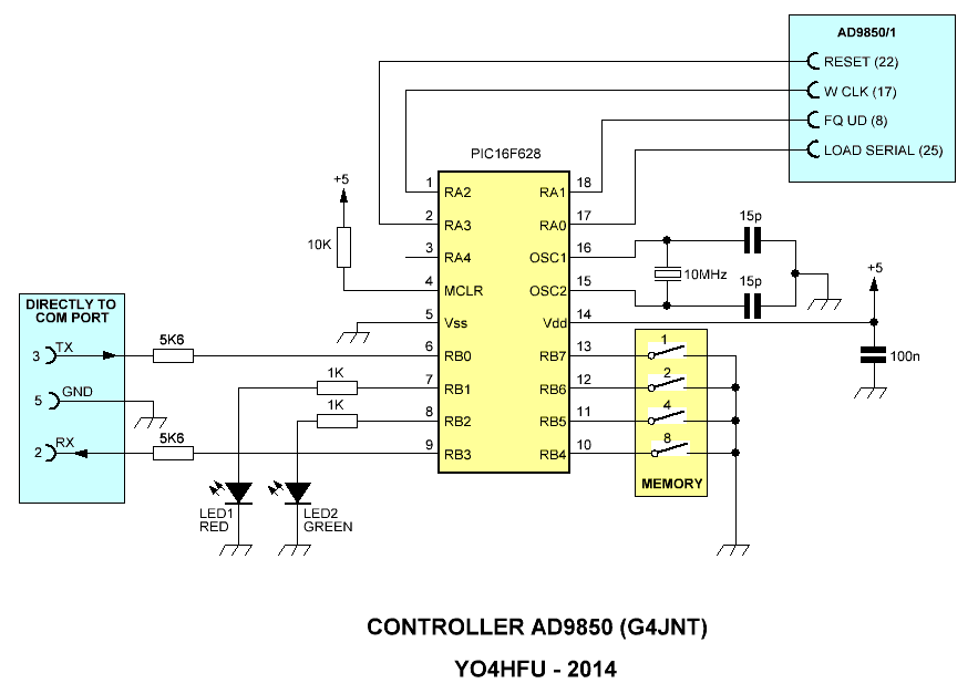
![]() RDDS PIC16F628 controller - basic schematic
RDDS PIC16F628 controller - basic schematic
Gallery:
![]() Top Side
Top Side
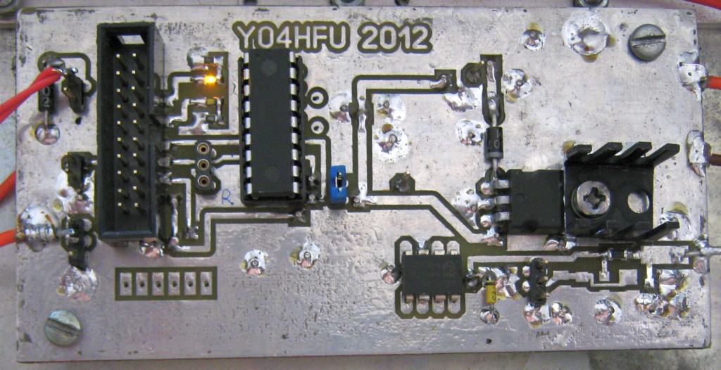
![]() Bottom Side
Bottom Side
![]() AD9850(1) Detail
AD9850(1) Detail