Page last updated May 5th, 2019
A basic low-pass filter was modeled to add to the output of the VFO to 'clean up' the output
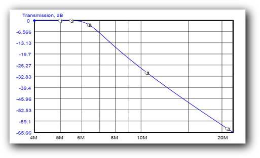
Marker 1 = 5.0 MHz - RL = 18.5 dB
Marker 2 = 5.5 MHz - RL = 28.5 dB
Marker 3 = 10.5 MHz - RL = 0.15 dB
Marker 4 = 21.0 MHz - RL = 0.002 dB
Marker 5 = 6.5 MHz - RL = 6.3dB
Marker 2 = 5.5 MHz - RL = 28.5 dB
Marker 3 = 10.5 MHz - RL = 0.15 dB
Marker 4 = 21.0 MHz - RL = 0.002 dB
Marker 5 = 6.5 MHz - RL = 6.3dB
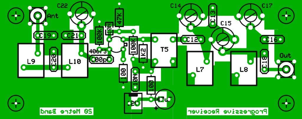
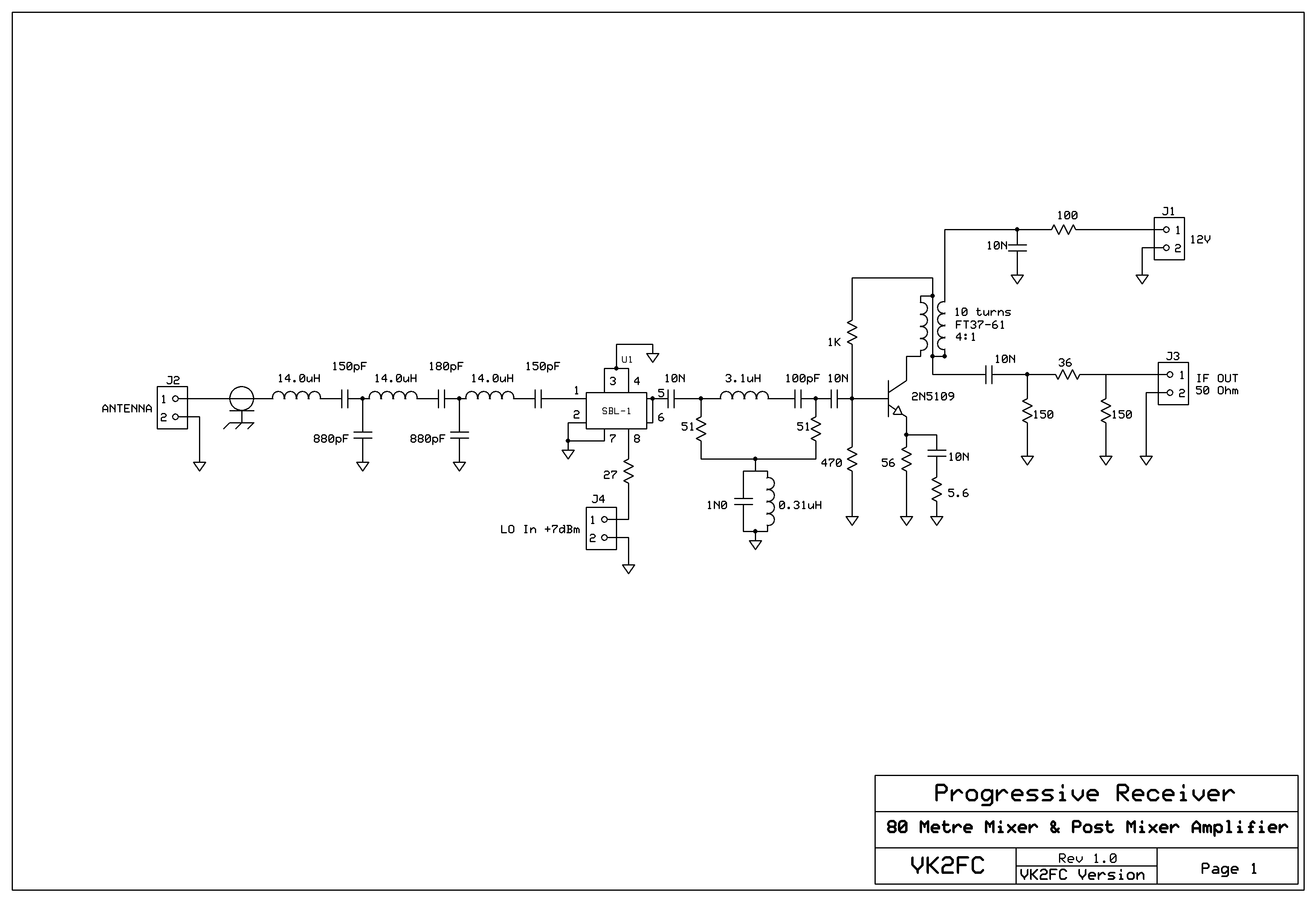
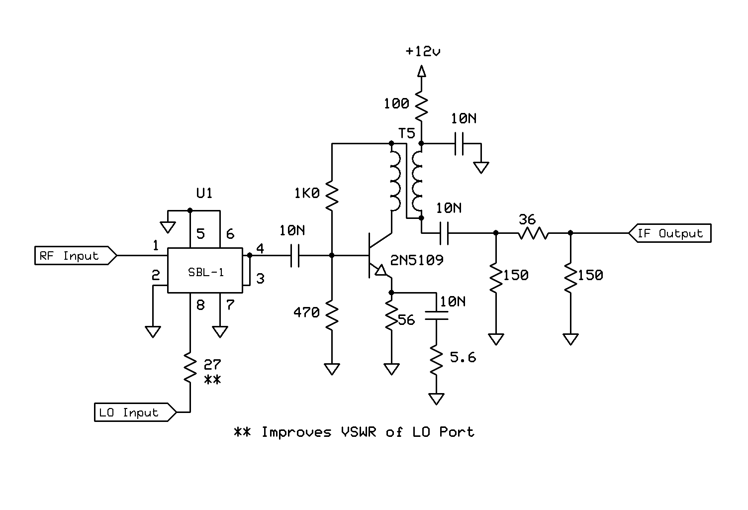
The Progressive Communications Receiver from November 1981 QST


There is significant distortion from the output of dual gate FET VFO buffer, I temporarily reduced the coupling capacitor from 10pF to 6P8 with little improvement. Also adjusting the gate 2 voltage had little effect except for reducing the output level so it was decided to add some filtering to the output as there is adequate output level. See below.
My first steps in this project were the I.F. amplifier then VFO construction in April 2018
No more progress(ive) updates to come!


A bit more progress today due to having a pre-formed chassis in the 'junk box' that I had recently earmarked for this project so it has now been pressed into service. I acquired this chassis in 1998 for another project that seemed important at the time but did not eventuate. I also had an unused Eddystone 898 slide-rule dial that is suited to this project too. Below are some photos of today's (Saturday afternoon's) endeavours. Fortunately for me, I had the original drilling template for the dial. Nibbling out the rectangular hole in the front panel was a time consuming process that I was not looking forward to but after an hour or so it was done! Just a bit of filing afterwards to tidy up the cut-out.
Saturday, 14th April 2018
The next step for this project is to settle on the rest of the receiver's layout before drilling too many holes in the chassis that may not be needed or drilled in the incorrect place! For the front panel, I need to allow for an S-meter, band change switch, AF and RF gain controls, preselector peaking, as well as a headphone socket, RIT etc etc..... Anything else? A notch filter would be nice too!
Today I drilled some PCB mounting holes in the chassis and also etched and drilled some more printed boards for this project. The 80 metre preselector/mixer and the convertor mixer board as well as the 40, 20, 15, 10 metre converter boards. Some photos of the boards prior to drilling are displayed below.


Sunday, 15th April 2018
Today I finished loading the components onto the detector/audio PCB. My version of these stages are different from the original article in that I've used an LM386 as the audio power amplifier. I have not tested this variation prior to this PCB build but I will test, verify and post my results here. My concern is whether I will have enough audio level to drive the LM386 effectively. The LM386 is not the best of choices as far as distortion and output power but it does do a reasonable job and I have a number of them in the parts bin. I've also had a bunch of the Mini-Circuits SBL-1 mixers in my possession since the early 1980's and used very few of them until recently. My next step is to load the components onto the 80 metre mixer PCB as well as the 2nd mixer PCB.
Over this weekend I also spent a couple or more hours on the chassis layout and where to locate some more of the printed boards as well as work out the 80 metre preselector tuning physical layout. I needed to keep the preselector capacitor as close as possible to the preselector PCB which is situated directly behind the VFO compartment but also needed the adjustment knob to be in a suitable position on the front panel. I had the two pulleys and belt already. They were left overs from another projects from years ago.
The two variable capacitors are identical with a maximum capacitance of 420pF. I would have preferred physically smaller ones but these are what I had in my parts collection. It's good to be able to put them back into useful service finally!


Friday, 20th April 2018
I've finished loading the components onto the 80 metre preselector/mixer board, the converter mixer board and the BFO board. I'd really like to use crystal oscillators instead of a DDS option for the converters but as yet I have not investigated the feasibility and cost of doing this.
A PCB artwork has been completed for a relay board which will take care of band-switching instead of using a multi-wafer rotary switch which I don't have. A small amount of DC current will be passed through each of the relay contacts whether open or closed. This to aid in contact longevity.
Getting closer now to be able to do some testing of the core 80 metre receiver. The RF and AF gain control pots were purchased from my local Jaycar Electronics store during the week so will fit them and begin wiring up the PCB interconnections at the weekend.
This afternoon the rear panel was fitted and some more holes drilled into the front panel to accommodate the various potentiometers and the 'S' meter. I'm going to use an old style 500uA FSD for the S-meter. I'll have to redo the existing 0-500 scale to make it look like a signal strength meter.
Wednesday, 25th April 2018 (Anzac Day)


Saturday, 28th April 2018
A power supply PCB artwork was designed last night. I allowed for three supply rails. +/- 12V and 9V. Actually there are two isolated +12V rails. I'll dedicate one to the detector and audio amplifier PCB to improve isolation and decoupling from the other receiver circuits. I'm not sure yet if I will need the -12V and +9V but who knows what additional features may get added in the future!
A bit more time spent on the front panel this afternoon. I fitted some of the controls and S-meter etc. to review the layout.
The 80 metre mixer stage was checked this evening with the spectrum analyser and tracking generator. Focusing mainly on the passband filtering stages ahead of the SBL-1 mixer. The preselector tuning capacitor adjusts the peak response between 3 and 4 MHz and that seems fine. However the skirts are not as steep as I expected and the attenuation either side of the peak not overly deep. The low pass section of the filter is functioning as expected. Insertion loss was measured as 6dB at 3MHz and 9dB at 4MHz. Allowing for some mismatch with my sampling technique let's say 3-6dB across the band. I will do so more tests with a 2nd board I have built and the output of the filter terminated not with the SBL-1 mixer but a 50 Ohm 10dB attenuator at the input port of the analyser.
I'm curious to know whether the same (or lesser) attenuation results can be achieved with a broadband filter design.
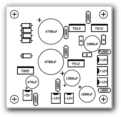
Power Supply PCB Overlay
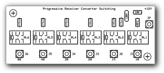
Band Switching Relay PCB Overlay


Powered up for the first time as a 'complete' receiver. With just a couple of metres of hook-up wire as an antenna I could hear some weak SSB signals on 80 metres. A quick check with the signal generator revealed all is OK and it can 'hear' down to at least 0.1uV. Audio from from my modified audio board using an LM386 sounds clean and distortion free with adequate volume for the 4" speaker.
1st May 2018
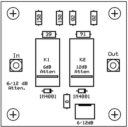
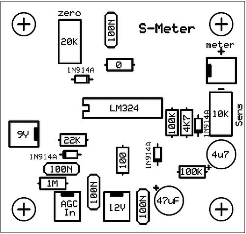
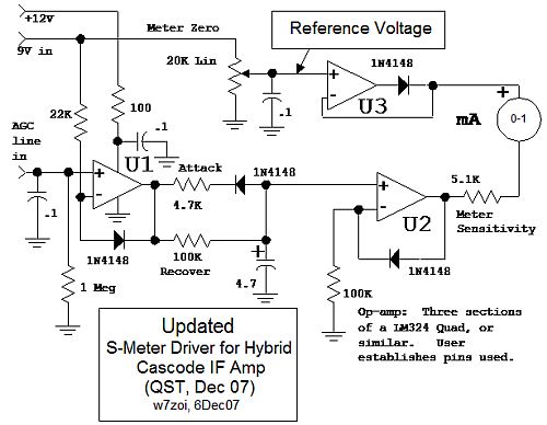
PCB artworks have now been done for the two boards below. I hope to etch, build and fit these at the weekend. The overlay on the left is a 6/12db 50 Ohm attenuator which can be switched in or out as required and provide either 0, 6, 12, 18 dB of signal attenuation. The overlay on the right is an S-meter driver circuit. A bit of 'googling' found the circuit on a W7ZOI web page. It is intended for use with the I.F. amplifier used here or the HYCAS I.F. amplifier circuit. My build of the HYCAS I.F. can be seen here.
Saturday, 5th May 2018
More front panel controls have been added as well as some grommets around the chassis to assist with cabling between the printed boards. The attenuator and S-meter printed boards were etched today and mounted in their respective locations. The attenuator is located on the rear panel adjacent to the antenna connector and the S-meter PCB has been mounted on the under side of chassis directly below the I.F. amplifier. This is a convenient location to pick up the AGC Voltage from the I.F. board and keep the interconnection wire as short as possible.
I've been giving more thought about where & how to place the four preselector boards, mixer board, band change relay boards and the four crystal oscillators. The only place for most of these to go is on the underside of the chassis. The underside is only 40mm deep. I already have the power supply board and meter driver board in position there so a total of 12 boards to be housed on the underside. It will be tight!
The PCB artwork for the crystal oscillators was completed early on Saturday. I was able to fit three oscillator circuits onto this size PCB so I will need two boards for the additional 5 bands. The board dimensions are 100mm x 60mm. A quick 'touch-up' with the pen in a couple of places and the board will be ready for etching.
The PCB artwork for the crystal oscillators was completed early on Saturday. I was able to fit three oscillator circuits onto this size PCB so I will need two boards for the additional 5 bands. The board dimensions are 100mm x 60mm. A quick 'touch-up' with the pen in a couple of places and the board will be ready for etching.


Not too much progress today due to other commitments although I did manage to etch two of the heterodyne oscillator PCB pictured above and make an aluminium plate/bracket to hold the 4" 4 Ohm speaker on the right rear side of the chassis. It sounds simple but took me exactly 1.5 hours to measure, manufacture and fit this plate and speaker to the chassis!
Sunday, 6th May 2018
Tuesday, 8th May 2018
The two crystal oscillator boards have been drilled and I've settled on the 5 bands I wish to add to the core 80 metre receiver. I will order the crystals today as it is a 5 to 6 week wait from Hy-Q Crystals in Melbourne. The bands are 40,20,15 and 10 metres, however 10 metres will be two 500KHz segments from 28 to 29 MHz. I'm uncertain as yet whether one preselector PCB will suffice or I'll need two to achieve the necessary bandwidth so will do some testing. It must be years since I bought crystals as they were around 20 bucks each last time and now they are $46.50!!!
I had considered the idea of adding a 6 metre converter for one of the bands but I'll save that idea for another project.
I had considered the idea of adding a 6 metre converter for one of the bands but I'll save that idea for another project.
5 crystals were ordered yesterday and now a 5 to 6 week wait until they arrive. I'll use this time to finish off the wiring of the core receiver as well as load the remaining boards with components. I also need to give consideration as to where they will be placed on the underside of the chassis which is only 40mm deep.
The image above is one of the filter/preselector boards that are required for each of the extra bands. I'll work my way through finishing each off and doing an alignment to see how the pass band looks. I plan to utilise the 40673 MOSFET RF amplifier for all bands except 40 metres which will have no gain before the mixer.
The image above is one of the filter/preselector boards that are required for each of the extra bands. I'll work my way through finishing each off and doing an alignment to see how the pass band looks. I plan to utilise the 40673 MOSFET RF amplifier for all bands except 40 metres which will have no gain before the mixer.
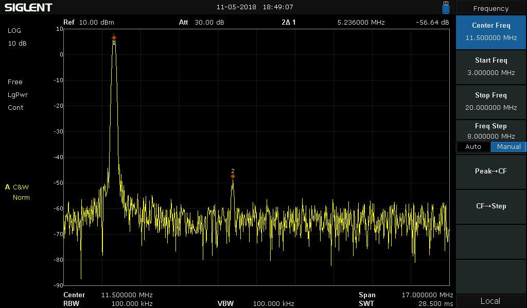

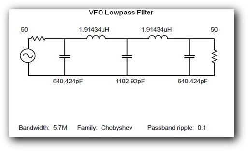
As a bit of a diversion, I redesigned the VFO low pass filter today and was pleased to see significantly lower harmonic levels at the output as compared to the output from the previous filter in the screen capture in the above left. The 2nd harmonic is now almost 57dB below the 5 MHz VFO carrier as opposed to 38dB previously. I guess it's of no real benefit but I did it just to see what could be achieved. The new filter circuit can be seen below. It's been fitted inside the VFO enclosure.
Friday, 11th May 2018


Saturday, 12th May
All four preselector boards have been assembled as per the photo below. The leftmost is the 10 metre board and the rightmost is the 40 metre board. A 40673 RF amplifier has been included for all bands except 40. The board on the lower right is one of the two 'band switches' that will select the preselector for the appropriate band. A similar board will connect the crystal oscillators to the 1st mixer board.
All four preselector boards have been aligned with a spectrum analyser and tracking generator and the plots can be seen below. The alignment was a bit difficult to get the desired response. It would have been very time consuming without the test gear mentioned above. None the less, it can be done by monitoring either AGC Voltage or recovered audio and tuning at the centre and upper and lower band edges.
A good starting point for the alignment is to adjust the coupling trimmer capacitor for minimum capacitance then peak the remaining trimmer caps for maximum gain at the upper band edge. Once done adjust the coupling capacitor for the desired bandwidth monitoring the lower band edge frequency. A further small adjustment to the bandpass tuning is necessary to get some 'balance'.
I'm curious to know why the 40 metre filter response's upper skirt is the shape it is. I think it may be due to the low pass filter fc being too high. The overall attenuation is also too high so further investigation is warranted.
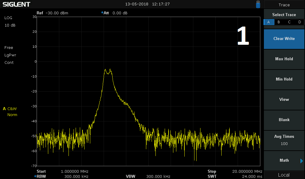
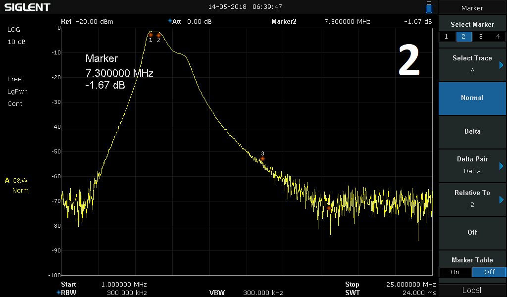
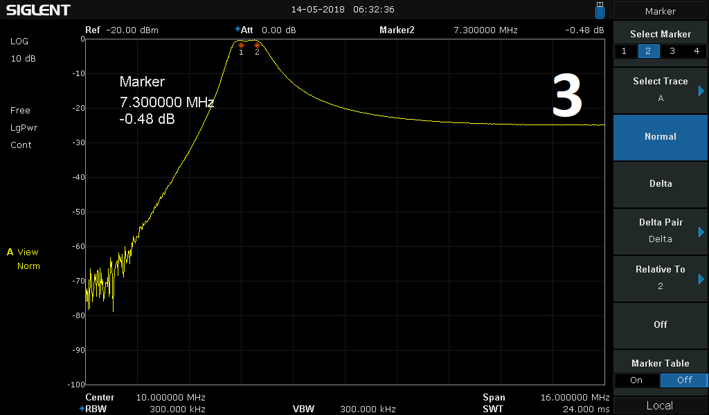
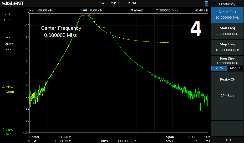
I had concerns about the 40 metre preselector attenuation & response above so I used 'Elsie' from Tonne Software to model a bandpass filter for 6.8MHz to 7.3MHz which is going to be the tuning range for my receiver's 40 metre band. Referring to the images below.
1. Is the original first-built response
2. Is the response of the modified filter
3. Is a sweep of the bandpass section only of the modified filter
4. The yellow trace is the bandpass filter only and the green trace is both bandpass and lowpass
Notice there is less attenuation now and a flatter response from 6.8 to 7.3MHz so I'll go with this modification.
I inadvertently started this project in April of 2016 by building the I.F. amplifier circuit on a homemade PCB. The 9 MHz SSB filter was removed from an old Wagner marine HF radio years after it was removed from service. The original idea was to use the I.F. amp in something other than this receiver. However, over time, I warmed to the idea of building the whole receiver. Anyone that has built a receiver like this will know how much time and effort is required. It's been an enjoyable & eventually rewarding project. After overcoming a few minor issues throughout the build and a bit of circuit customisation, I am now very happy with the performance of this receiver design and can recommend it to anyone who is contemplating building it.
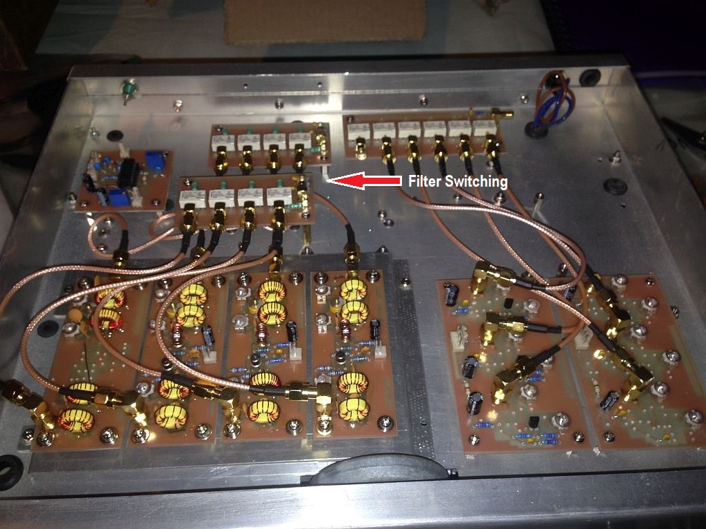
The circuit below includes a switchable RF attenuator and antenna switching. The antenna is connected directly to the 80 metre receiver front end when the band switch is set to 80. If one of the other bands is selected the antenna will be switched to the RF filter for that band and 1st Mixer via a band filter switching PCB then coupled back to the 80 metre receiver. A small amount of current flows through the relay contacts when activated to prolong contact life. Now that the switched 6dB/12dB RF attenuator is included on this PCB, the one described further up this page will not be required. This PCB has now built and tested.
Monday, 21st May 2018


I had a couple of hours to spare so made up a sub-chassis to mount the 40, 20, 15 & 10 metre filter boards on the underside of the chassis. The idea behind the sub-chassis is to reduce the total number of holes drilled through the main chassis as well as having to avoid all of the other M3 bolts & nuts already mounted through the main chassis. Six more PCB's to be fitted on the underside. It will be tight!
Click to download the article


Weekend, 26-27th May 2018
I've decided to rebuild the two band-switching relay PCB to reduce the switching capacity to 4 rather than the original 6 converters I had planned for. The main reason behind this is to reduce the physical size of the boards. Artwork, etching has been completed. I will need to transfer some components from old PCB to new.
The two crystal oscillator boards have now been mounted on the underside of the chassis.
An alternate design for the 40 metre band filter has been built and bench tested. It's a meshed capacitor-coupled bandpass designed with 'Elsie' software. See below. I'm unsure whether it will be used in this receiver. The frequency response/shape is quite good but the attenuation is slightly higher than the one in the original design. I will do some comparisons between the two in the future.
The RF attenuator and 80 metre band switching PCB has also been built and tested. It is the image on the 2nd from right below.
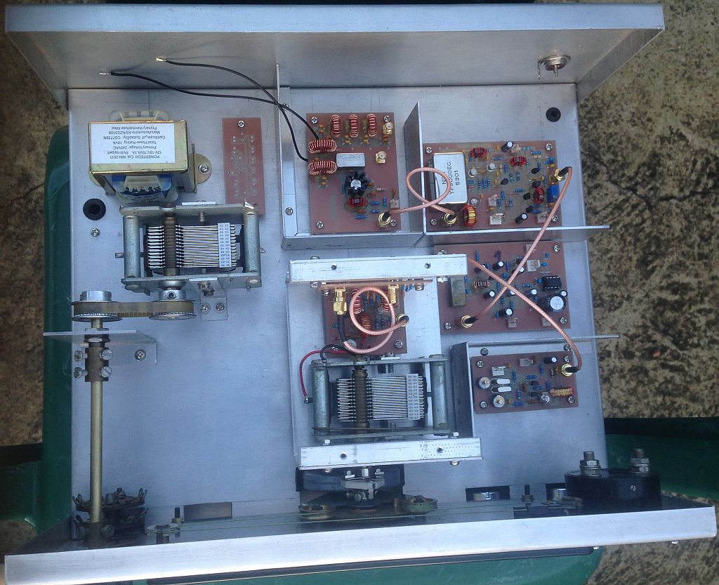
All of the printed boards have now been fitted to the chassis which will allow me to make up the wiring loom. A couple of boards still need to be drilled and have the components loaded.
The two crystal oscillator boards have now been mounted on the underside of the chassis.
An alternate design for the 40 metre band filter has been built and bench tested. It's a meshed capacitor-coupled bandpass designed with 'Elsie' software. See below. I'm unsure whether it will be used in this receiver. The frequency response/shape is quite good but the attenuation is slightly higher than the one in the original design. I will do some comparisons between the two in the future.
The RF attenuator and 80 metre band switching PCB has also been built and tested. It is the image on the 2nd from right below.
All of the printed boards have now been fitted to the chassis which will allow me to make up the wiring loom. A couple of boards still need to be drilled and have the components loaded.


Saturday, 2nd June 2018
The two new filter switching relay boards have been drilled and components loaded. The crystal oscillator boards have also been completed and ready to test once the crystals arrive.
I've ordered an old style 10K switched potentiometer from the USA so that I can switch the 240AC supply on and off via the volume control knob. I searched my junk box but could only find high value units of 500K or above.
This receiver is now at the stage where it can have a DC wiring harness made up and fitted permanently. A nice job to pass a few hours during one of these Winter evenings!
Some additional shielding will be added between the front-end filter PCB's and the crystal oscillator PCB's below.
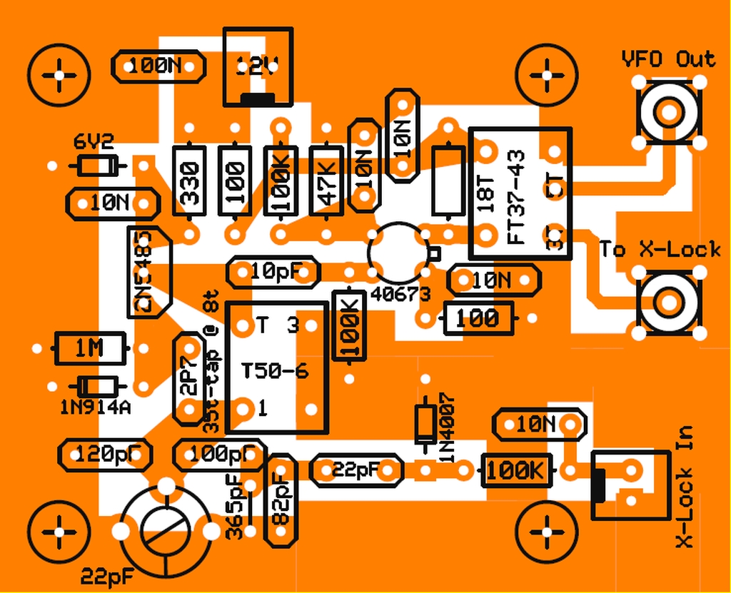
A modified version of the VFO was built today. This version switches extra capacitance into the circuit via PIN diodes to change the frequency by approximately 3 KHz when the opposite sideband is selected by way of switching BFO crystals. More testing needs to be done to ensure that VFO frequency stability has been maintained.
Initially I installed a Motorola MPF102 as the oscillator, which is one of the recommended choices in the publication but the circuit would not oscillate. Actually I tried up to 3 MPF102 purchased from different sources without success. So I checked my original build and for some reason I had used an 2N5485 in that circuit. I soldered in a 2N5485 and my new board oscillated straight away. I'm really curious to understand why the MPF102 will not oscillate!
Initially I installed a Motorola MPF102 as the oscillator, which is one of the recommended choices in the publication but the circuit would not oscillate. Actually I tried up to 3 MPF102 purchased from different sources without success. So I checked my original build and for some reason I had used an 2N5485 in that circuit. I soldered in a 2N5485 and my new board oscillated straight away. I'm really curious to understand why the MPF102 will not oscillate!
Weekend, 9th & 10th June 2018

I've decided to update this VFO PCB design even further to make provision to add a huff n puff VFO stabiliser circuit in the future. It will incorporate a 2nd RF output port as well as an input to a varicap diode.
Tuesday, 12th June 2018
The VFO artwork has been redesigned yet again and a PCB has been made for the latest version of the VFO circuit which incorporates an additional RF output and DC input to allow for an optional VFO stabiliser circuit to be fitted.
Monday, 2nd July 2018
The crystals for the band converters that were ordered in early May finally arrived today. I spent a few hours in the shed making the top and bottom covers for the receiver. There is not much to stop me completing this project now as all of the metal work has been completed.
A speaker grill pattern has been drilled into the side of the receiver's top cover. A lid from an old CB radio with speaker pattern perforations was bolted to the area and used as a drilling template. I'm quite pleased with the result.
A speaker grill pattern has been drilled into the side of the receiver's top cover. A lid from an old CB radio with speaker pattern perforations was bolted to the area and used as a drilling template. I'm quite pleased with the result.


Searching the internet I found a circuit for a marker oscillator that use a 6.4 MHz crystal and a CMOS divider IC. A PCB has been made for this circuit and it will be incorporated into the receiver for a switchable frequency reference of 25KHz or 100KHz.
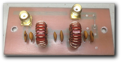
The filter has provision for a resistive attenuator at the output to reduce the VFO level after filtering to around +7dBm to the present to the local oscillator input of the SBL-1 balanced mixer. Values were selected to provide 4dB of attenuation. I used NPO ceramic capacitors which were on hand.
The images below show the output sine wave and harmonic content from the VFO before and after filtering with the lowpass filter with an FC of around 6.5 MHz. The filter was modelled with 'elsie' from Tonne Software.
The images below show the output sine wave and harmonic content from the VFO before and after filtering with the lowpass filter with an FC of around 6.5 MHz. The filter was modelled with 'elsie' from Tonne Software.
The assembled filter ready for testing
Saturday, 25th August 2018
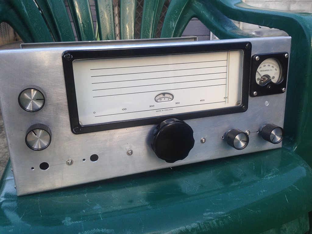
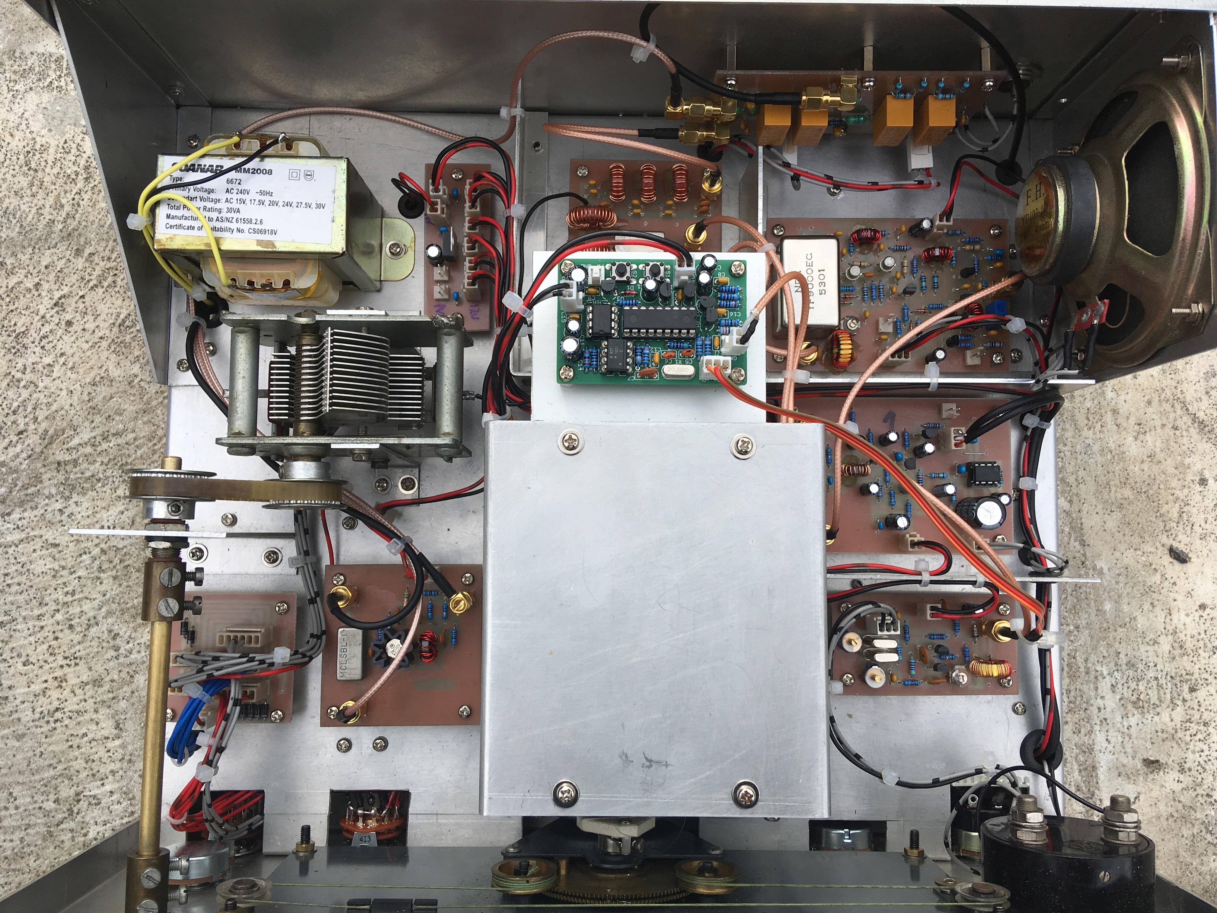
Today, after a break of quite a few weeks, I have completed the D.C. wiring of the 80 metre portion of the receiver and powered it up for some more testing. The image on the left below show the final state of the wiring on the top side of the chassis. The S-Meter is now yet functional.
Progressive Receiver
The wiring for the 80 metre band, which is the core of the receiver, has been completed and now awaits the 4 converters to be wired in.
Click Here For A Close-Up View
)
)
After another period of relative inactivity with this project, I've put quite a few more hours in and made some pleasing progress to get this close to completion. An "X-Lock" VFO stabiliser kit has been built and installed (above right) along with my modified 5 MHz VFO with the extra RF output for the X-lock as well as an input for applying the correction signal. The S-meter circuit has been wired and tested as well as the attenuator board on the rear panel. All co-axial cables and DC switching for 40 through 10 metre bands have been wired in. The crystal oscillators for 40, 20 and 15 metres have been installed and tested. All that remains to be built before completion are the two crystal oscillators for 10 metres.
The X-Lock was purchased from Cumbria Designs in the U.K. (which have since gone out of business). I'm very pleased with its performance and makes my homebrew VFO very stable. Only a few Hertz of drift was noted when left running overnight. You might ask "well why not use a DDS VFO" and the reason is that it would be difficult for me to combine the Eddystone dial with a DDS VFO.
The X-Lock was purchased from Cumbria Designs in the U.K. (which have since gone out of business). I'm very pleased with its performance and makes my homebrew VFO very stable. Only a few Hertz of drift was noted when left running overnight. You might ask "well why not use a DDS VFO" and the reason is that it would be difficult for me to combine the Eddystone dial with a DDS VFO.
27th, 28th October 2018
X-Lock stabiliser for VFO
Even though myVFO is quite stable over the short term I decided to fit this VFO stabiliser to add extra stability over the long term. The VFO PCB has been redesigned to make the integration easier.
Click Here For A Close-Up View
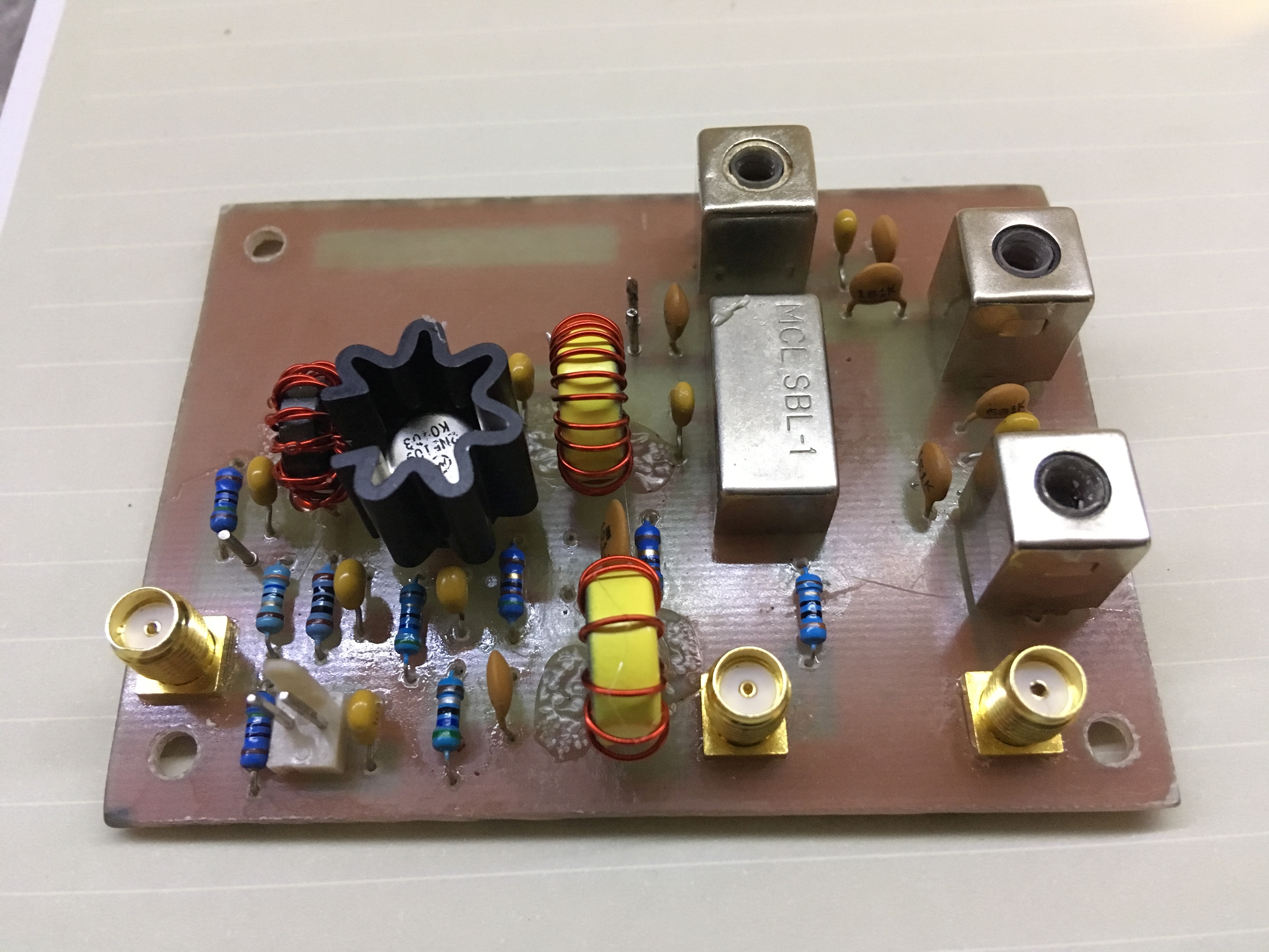
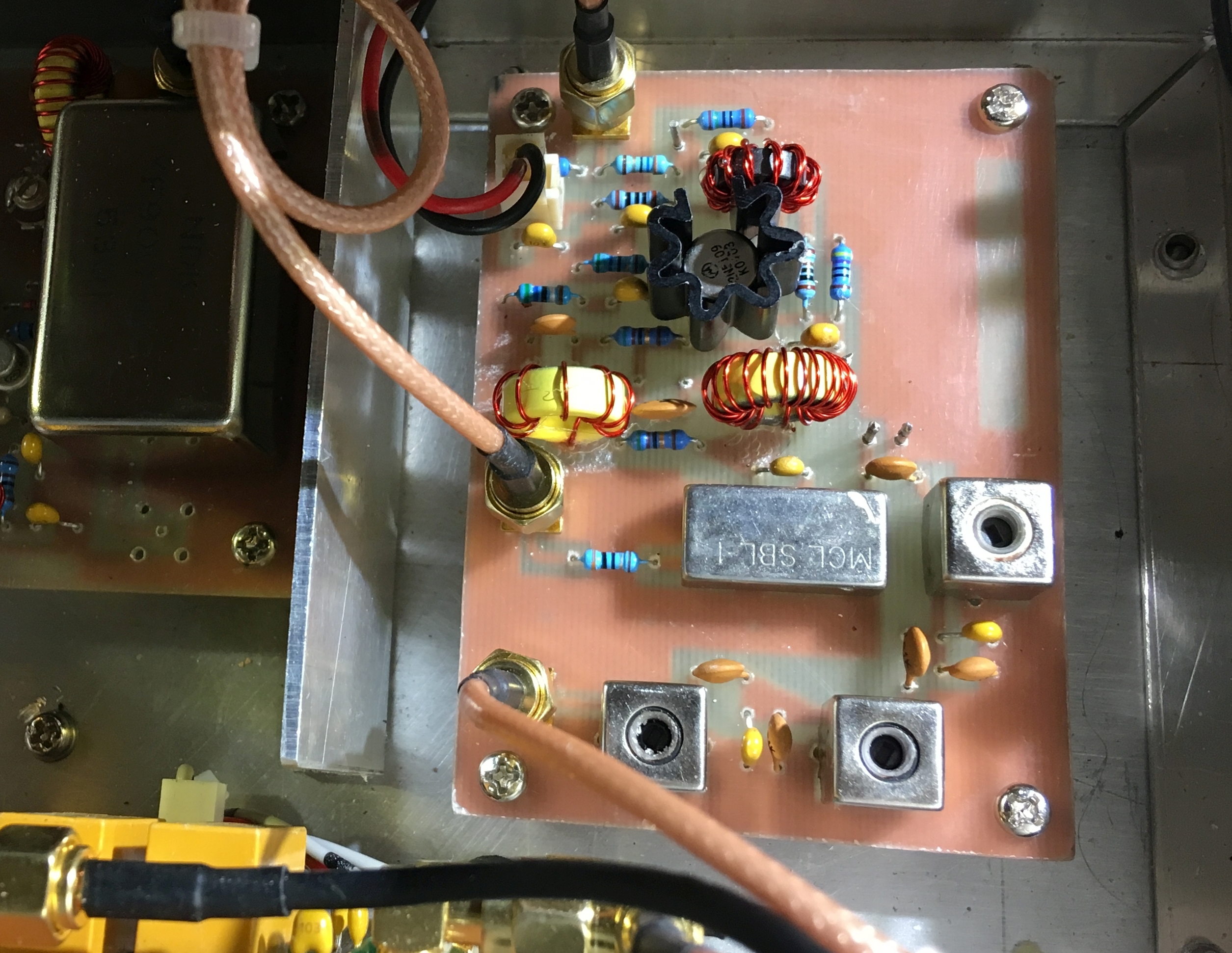
I have redesigned the 80 metre front end filter and mixer PCB in an attempt to reduce the unwanted mixer products that I believe are occurring there and generating 'birdies' all over the place, particularly on the higher bands. The 80 metre receiver is relatively free of these birdies. The new 80 metre bandpass filter is now fixed at a bandwidth of approximately 700 KHz so I can do away the pre-selector tuning capacitor used in the original design. I'm thinking that this new filter will provide a better termination at the RF port of the mixer too. The output of the SBL-1 mixer is now terminated by a 'bridged T' 50 Ohm diplexer. A PCB artwork was created and a PCB made & loaded with all components and tested today.
Once installed I was pleasantly surprised by the results. The receiver has good sensitivity over the entire 3.5 to 4.0 MHz portion of the band and all of the 'birdies' have gone! It seems to be as sensitive as the original design too. The images below are of the bandpass filter response and the assembled PCB.
Once installed I was pleasantly surprised by the results. The receiver has good sensitivity over the entire 3.5 to 4.0 MHz portion of the band and all of the 'birdies' have gone! It seems to be as sensitive as the original design too. The images below are of the bandpass filter response and the assembled PCB.
24th November 2018
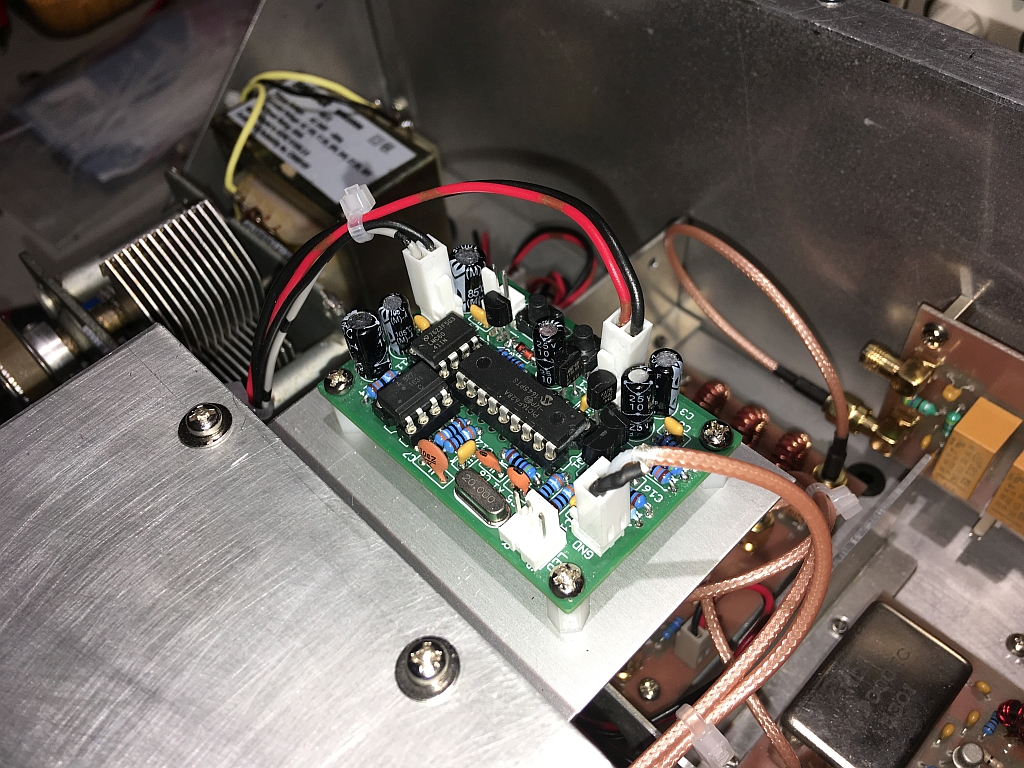
When testing the 15 and 20 metre band crystal oscillators I noticed considerable instability & spurious oscillations whilst adjusting the trimmer capacitors for maximum output. I could not find the 'sweet spot' where the frequency was correct and amplitude was stable. The original article stated that these adjustments are to be carried out when the oscillator is connected to the mixer and terminated. I checked my oscillator switching circuits for a potential problem that I may have introduced and even though a couple of changes were made the instability remained. Finally, I disconnected the oscillator output from the SBL-1 and connected it to a 50 Ohm termination. Upon retesting, the oscillators behaved perfectly but not when I reconnected them to the LO port of the SBL-1 mixer. Thinking about this for a while, I recalled the Rx mixer circuit of the Elecraft K2, where a low value resistor was placed in series with the local oscillator input to the balanced mixer. I figured this was to improve the termination to the mixer so I tried the same. I added 27 Ohms and to my surprise when retesting, the oscillators were now quite stable and predictable. I checked the return loss of the SBL-1 LO port and it was quite good. It appears that all is now functioning as desired. The image to the right shows where the 27 Ohm resistor was fitted in series.
As of today, Sunday the 28th October, I now have all six bands operational and everything is looking good. The receiver is quite sensitive on all six bands. A couple of strong internally generated 'birdies' are apparent on both 10 metre bands without an antenna connected so further investigation is warranted to see where/how these 'birdies' are being generated. One appears around 28.334 MHz and the other at 28.668 MHz. A couple of calculations and I discovered that Xtal Oscillator - VFO x 3 = 9 MHz, the I.F. frequency. I'll investigate this further as time permits.
Now that a new 80 metre band circuit board has been fitted I have removed the large variable capacitor that was used for signal peaking. A 25 KHz marker oscillator PCB has been fitted to the bracket that was left over after the cap was removed.
Click on any of these images for a closer look
First Mixer Circuit - Follows Converters
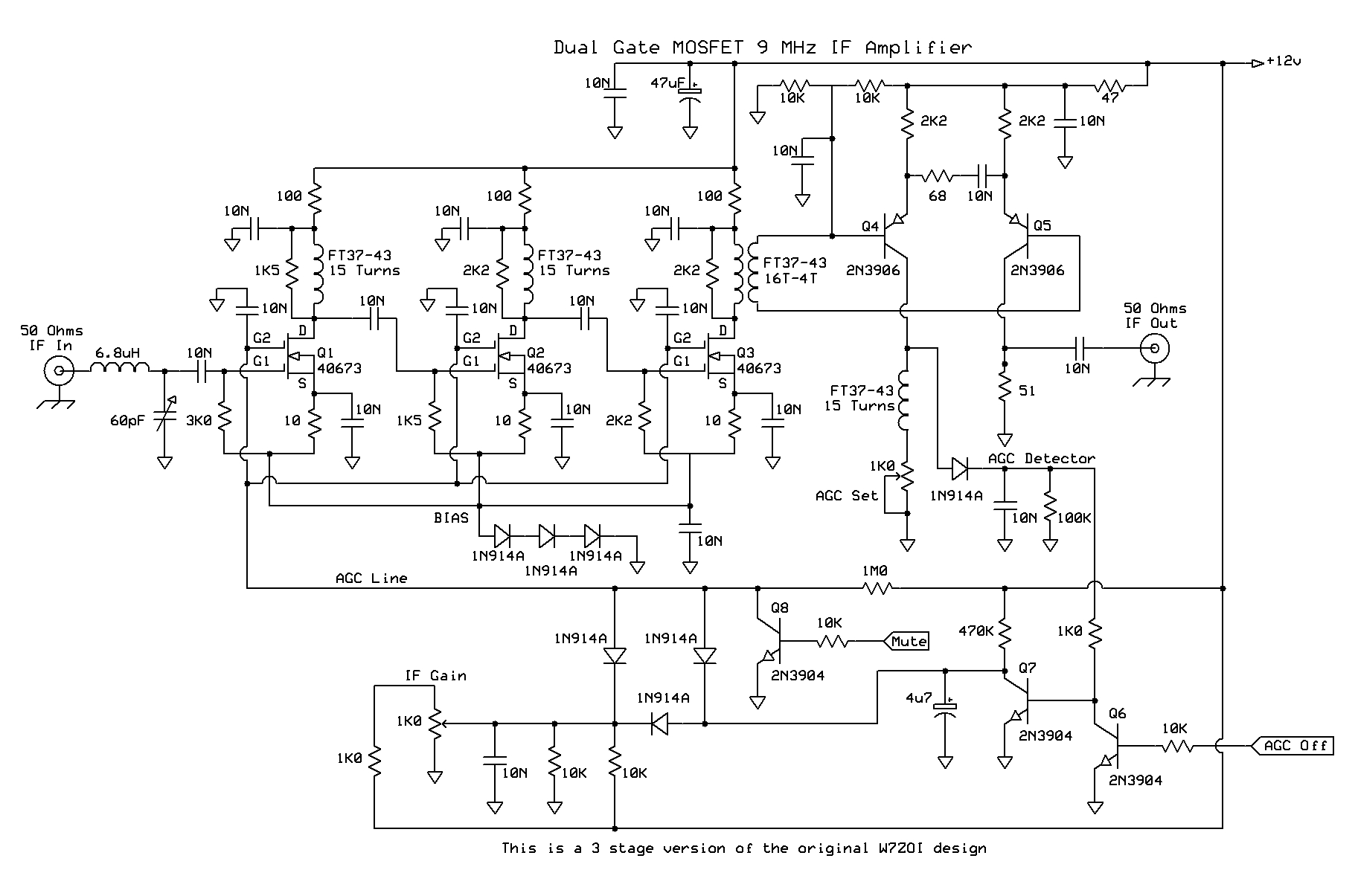
Compared to other designs I've studied and some measurements I have done on the original I.F. amplifier circuit as built, I found the overall gain including filter loss to be around 30dB. The original article does not give a gain figure for the design but I would expect to see around 20dB per stage less filter losses of 2dB or so in my case. There is also a reasonable amount of loss in the IF output half of the differential pair due mainly to the low impedance output of 50 Ohms, so the 30dB I have measured in my build may be correct. If you have built this circuit and can verify this figure I'd be pleased to hear from you.
In my version of this receiver, I have included R.F. amplifier stages on the 20,15 & 10 metre bands. The sensitivity on these bands is quite good but not so on 80 and 40 metres where there is no R.F. stage gain. As a side note, having an RF amplifier on some bands and not on others also poses a problem for maintaining S-Meter calibration due to the difference in system gain between bands.
In an attempt to improve overall performance, I have built a new I.F. PCB with three 40673 stages to give one extra stage of amplification over the original design. I guess it will be the dual gate MOSFET version of the well known HYCAS IF amplifer! I'll also give some thought to an S-meter 'correction' circuit for the bands with extra amplification.
5th of April 2019
More on the I.F. Amplifier Section
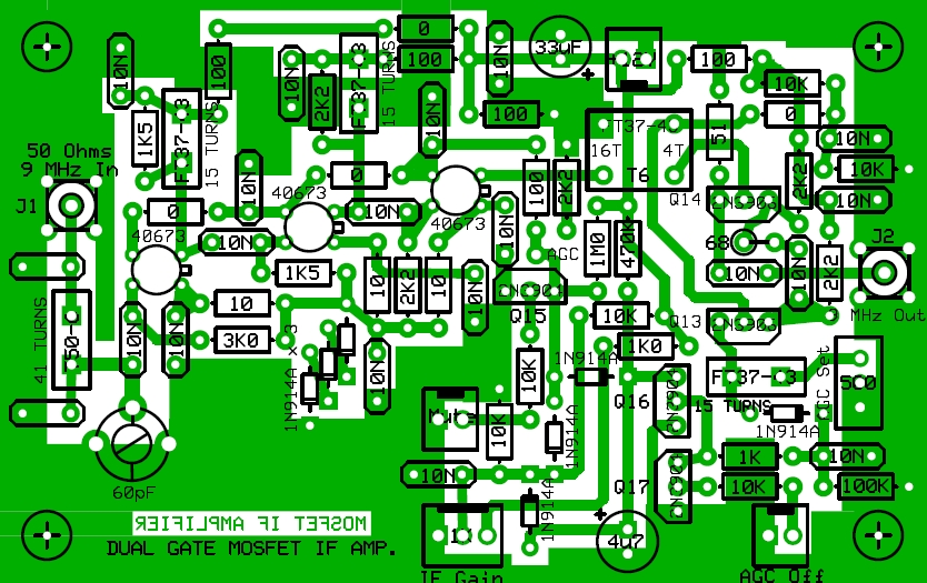
The new IF PCB layout to the left is the same size as my original build so it will fit onto the same mounting points in the receiver. There is no longer a space for the crystal filter on the board so it will mount on a smaller PCB located above the IF board with a shield between the two levels. The existing filter has a termination impedance of 500 Ohms so I will use transformers to match the filter to 50 Ohms of the mixer and IF amplifier. I've also done an artwork for another version using the BF998R dual gate MOSFET so I'm inclined to try that version too. The 'R' suffix is for mirrored pinout so I can mount them on the copper foil side of the PCB.
I have dedicated this project to my father, Ernie Millen, who passed away on the 11th of November 1981. He was solely responsible for igniting my interest in this fascinating hobby.

5th April 2019
Upon initial testing I had some instability issues (oscillating) without the AGC applied. The instability appears to be originating from the differential pair in the final stage although I'm not 100% sure just yet so further investigation is needed. It may be just a matter of too much overall system gain.
10th April 2019
With regard to the above, the value of the resistor in series with the capacitor that couples the emitters of the differential pair was increased from 22 to 68 Ohms and the instability is no longer evident. The overall gain including the crystal filter loss is approximately 50 - 55dB.
I think it would be wise to build this amplifier on a double sided PCB to possibly improve stability even though this single sided build works well.
| IF In | HYCAS Out |
MOSFET Out |
| -110 dBm | -55 dBm | -55 dBm |
| -100 dBm | -45 dBm | -48 dBm |
| -90 dBm | -35 dBm | -39 dBm |
| -80 dBm | -25 dBm | -30 dBm |
| -70 dBm | -15 dBm | -20 dBm |
| -60 dBm | -10 dBm | -15 dBm |
| -50 dBm | -10 dBm | -13 dBm |
To the left is a gain comparison (with AGC disabled) between the HYCAS I.F. amplifier I built and my homebrew 3 stage dual gate MOSFET I.F. amplifier. It shows that the MOSFET version has slightly lower gain over the range of input levels tested but this may be due to the fact that I have added 1500 & 2200 Ohm damping resistors across the drain chokes in the first two stages whereas the HYCAS design does not utilise resistors in those locations.
The new I.F. board has been installed in the receiver and I'm quite pleased with the receiver's performance now. I intend to do some measurements on the circuit to plot the gain control range.
The new I.F. board has been installed in the receiver and I'm quite pleased with the receiver's performance now. I intend to do some measurements on the circuit to plot the gain control range.
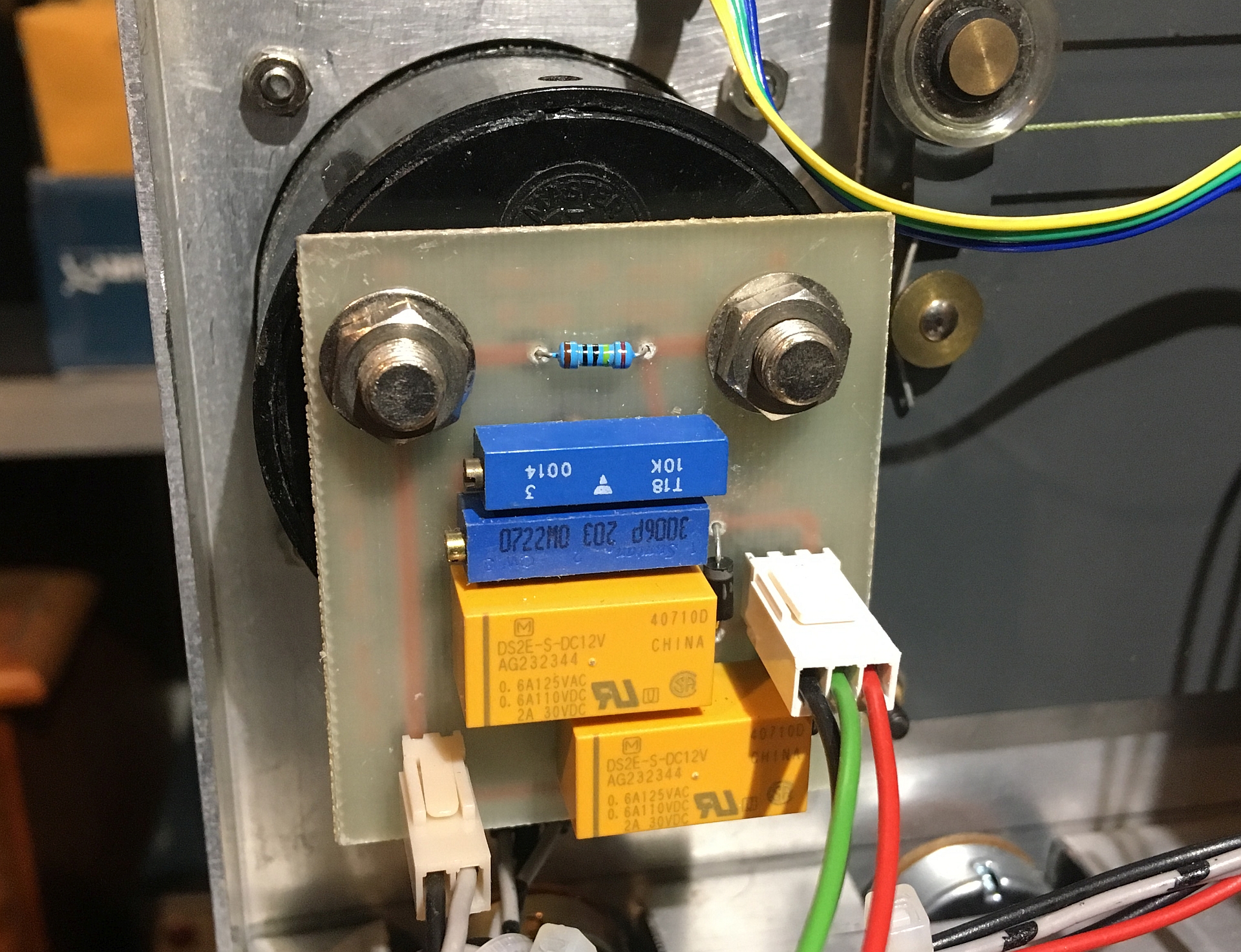
I built the circuit pictured to the left to correct for the difference in S-meter calibration between the various bands as it varied significantly from the 80 metre band reading when on 40 or 20,15,10 metres. The relays and associated trim pots are driven from the band switch. The reason for the differences in readings are due to the fact that all bands other than 80 metres have extra gain from the 1st mixer and band converters being switched in.
On 80 metres there is no extra gain as this is the core receiver.
On 40 metres there is extra gain from the 1st mixer stage.
On 20,15 & 10 metres there is extra gain from the 1st mixer as well as the 40673 MOSFET RF amplifiers.
On 80 metres there is no extra gain as this is the core receiver.
On 40 metres there is extra gain from the 1st mixer stage.
On 20,15 & 10 metres there is extra gain from the 1st mixer as well as the 40673 MOSFET RF amplifiers.
S-Meter calibration is initially carried out on 80 metres using the adjustment located on the S-Meter circuit further up this page. Then switch to 40 metres and adjust the 40 metre trimpot on the correction circuit PCB for the same reading. Finally switch band to 15 metres and adjust the 20,15,10 trimpot for the same reading. A level of 50uV was used as the reference signal for each band.
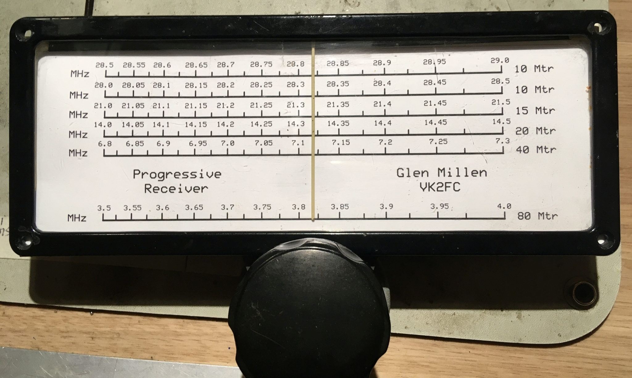
After one year in the making, this project is finally nearing completion. All that remains to do now is paint the case, label the front panel and apply the dial overlay above to the the Eddystone dial.
5th of May 2019

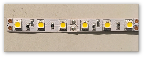
A length of adhesive backed 12 Volt LED strip was purchased from Jaycar Electronics. It was affixed to the front of the VFO enclosure to provide some dial backlighting. I will also investigate the possibility of adding a back light to the S-meter.
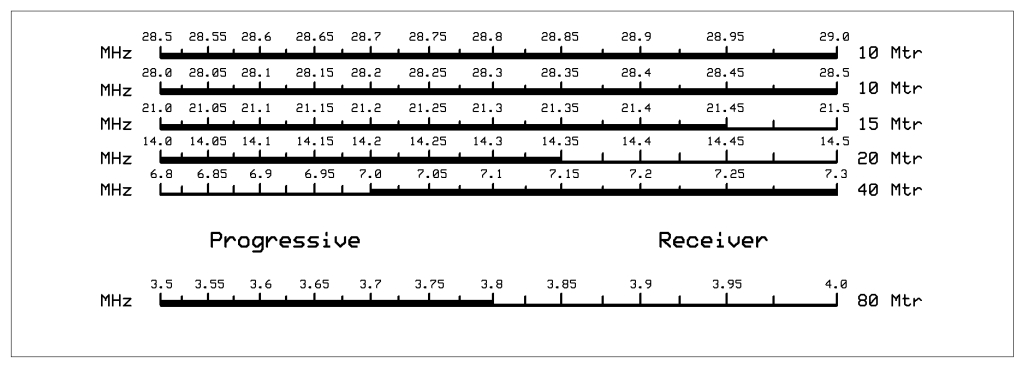
I used Express PCB to produce this dial overlay for the Eddystone 898 dial in my receiver. I'll print it onto adhesive backed white cardboard stock then apply it to the original plate on the dial. It took 3 or 4 hours to do the lay out.
Another version of the dial overlay placed on a spare 898 dial I have to see how it looks prior to fitment to the receiver