-- Dr. Ralph Taggart, WB8DQT, The ARRL Image Communications Handbook, 2002
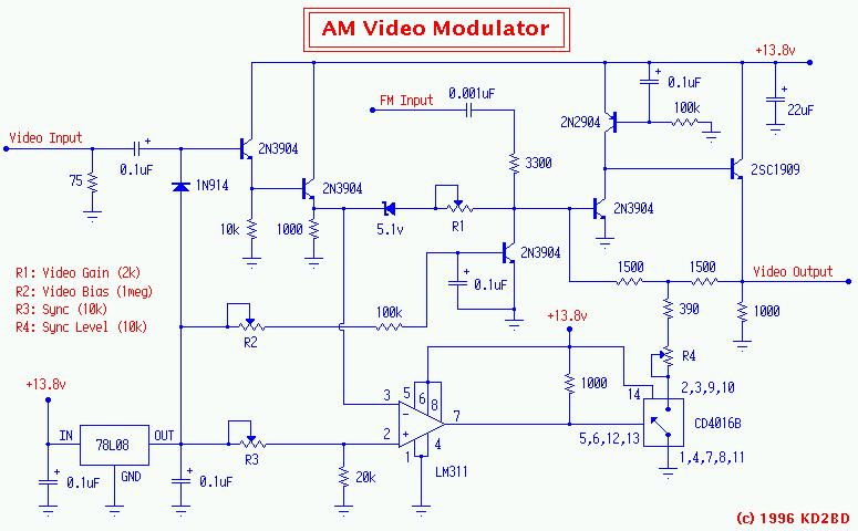
Building an in-band, duplexed ATV repeater system is not a trivial task. Just ask anyone who's tried. The output spectrum of the repeater's transmitter must be extremely clean, and both the transmitter's output as well as the receiver's input must be tightly filtered to achieve adequate isolation and reject interference from strong signals on neighboring frequencies.
When the Brookdale ATV Repeater System was first constructed, a PC Electronics model RTX-70 exciter was used in the transmitter portion of the repeater. However, the intermodulation distortion products generated by the exciter when amplified by a Mirage D100ATV-R amplifier were so severe, they completely overwhelmed the repeater's receiver, despite the extensive combline and interdigital filtering used in the system.
After much study and research, the cause of the exciter's strong IMD products was found to be the result of distortion and non-linearity in the exciter's video modulator, and not the modulated RF stages themselves. Once the original video modulator was replaced with the one described on this page, the harmful effects of IMD were reduced to imperceptible levels. An added bonus was a noticeable increase in the exciter's RF power output.
The clamped video is then level shifted through a zener diode and applied to a single video amplifier stage. A PNP transistor in the collector circuit functions as a constant current source for the video amplifier. The use of a constant current source rather than a collector load resistor in the video amplifier results in very high voltage gain with nearly rail-to-rail output voltage capability. Negative feedback around the video amplifier reduces the gain to the amount required, while it increases the bandwidth, flattens the frequency response, increases the linearity, and reduces any distortion products to extremely low levels.
A 2N3904 in the base circuit sets the `Q' point of the amplifier. FM subcarrier audio at 4.5 MHz is also injected at this point through a 3300 ohm resistor and a DC blocking capacitor. A high frequency 5-watt RF power transistor (2SC1909) serves as the last stage of the modulator. An NTE-235, NTE-236, or equivalent is suitable in this application.
Clamped video is also fed into an LM311 voltage comparator that serves as a video sync detector. Some builders have used an LM1881 sync separator chip for this stage. Either way, sync pulses detected by this circuit trigger a CD4016B silicon bilateral switch that lowers the negative feedback around the video amplifier and voltage follower at sync time to compensate for high power gain compression in any solid-state linear power amplifiers that may follow the video modulated stages. This method of sync expansion is unique in that it also compensates for audio subcarrier compression at sync time, resulting in a clean output signal with no sync buzz in the transmitted audio.
R1 is a video gain control. It is used to set the white modulation level. R2 is a video bias control. It is used to set the black modulation level. R3 is adjusted so that the LM311 delivers clean sync pulses to the CD4016B with an input signal present. R4 adjusts the sync modulation level. Up to 9 dB of sync expansion is possible with this circuit.
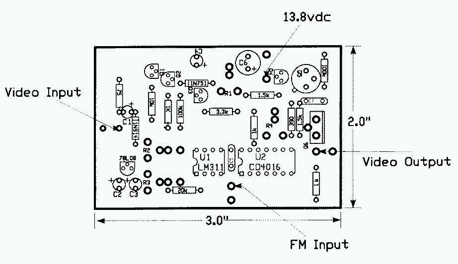
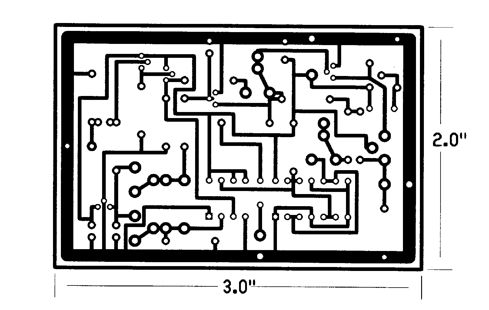
David Sudduth, KB0ZNP, was kind enough to develop a PC board design for this modulator using Circad 98 software, and offer the layout and foil patterns to anyone who wishes to duplicate this modulator. The original Circad 98 PCB data file is also available.
The following graphs show the results of a computer simulation of the video modulator when adjusted for a voltage gain of 20 dB. This simulation was performed using MicroCAP IV software, an electronic circuit analysis program by Spectrum Software.
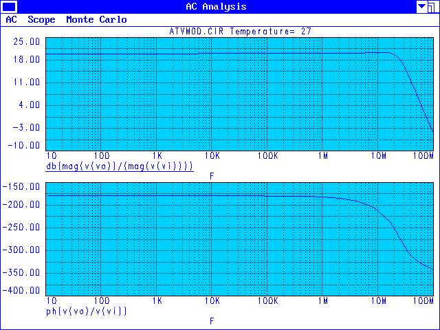
The top graph plots modulator voltage gain as function of frequency. The graph shows a wide and flat frequency response that extends to 20 MHz.
The lower graph plots modulator phase shift as a function of frequency. the graph shows a wide and flat phase response that is essential for accurate color reproduction. The phase response around the chrominance subcarrier (3.58 MHz) falls well within the +/- 10 degree specification used by commercial broadcasters.
|
|
John Magliacane |
