TCXO and associated components
Programming the Exciter (with
EEPROM contents example)
Hexadecimal conversion
spreadsheet
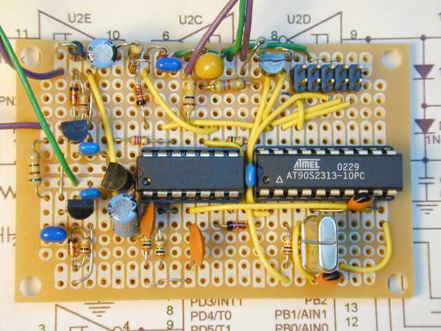
"Bare Bones" exciter
"All in One" DDS LowFER Transmitter
DDS
Exciter Using the Futurlec AT90S2313
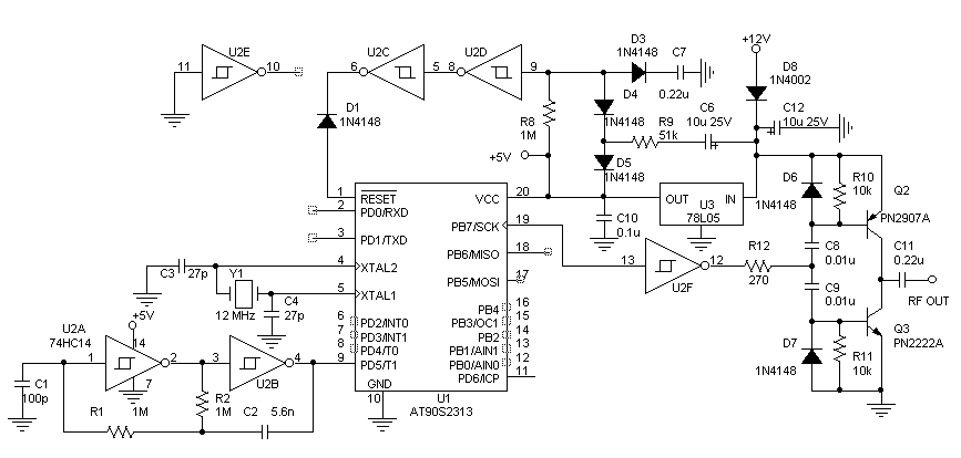
When I read the Internet article on "Building a Simple LF Exciter" by Murray Greenman, ZL1BPU, I decided that I had to have one! Direct Digital Synthesis (DDS) frequency generation has been around for quite a while, but most of the homebrew DDS projects are rather complex and use expensive chipsets. Murrays exciter has only 3 inexpensive ICs, and the whole thing can be built for under $50. Perhaps best of all, the exciter can be programmed via a PC to operate as a beacon, and the software is tailored for operation using modes that are popular among LF hams and experimenters. Murrays article is at http://www.qsl.net/zl1bpu/micro/EXCITER/Index.htm and there are also links to a very comprehensive users guide. His writeups are excellent, and you should view all of the information if you plan to build this project. I did a quick check of parts availability in the US, and quickly found sources for all of the ICs. To share the shipping/handling charges and to encourage more US LowFERs to experiment with the modes supported by the ZL1BPU exciter, I offered to purchase up to 10 sets of parts and to make them available at my cost. The offer was quickly "sold out". This article is intended to help those who purchased sets of parts to get their units running, and to provide ideas for anyone else who wishes to build this interesting and useful project.
Important Notice: As with any high-speed processor, it's easy for an undervoltage condition or a voltage transient to scramble the memory on the Atmel AVR chip. One fix for this problem is to add a voltage detector reset chip as described later in this article. Some time ago, Murray also suggested adding a 0.01 uF capacitor from the reset line (pin 1) of the microcontroller to ground. I found that this fixed a lot of problems, especially the apparent inability to load the EEPROM memory correctly. Unfortunately I never got around to updating the circuit diagrams or including a mention of this fix in my article. Maybe someday I will make the addition to the diagrams. In the meantime, I strongly suggest adding the 0.01 uF bypass capacitor on the reset line!
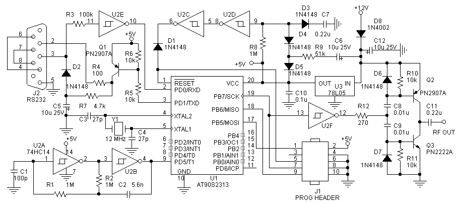
My version of the ZL1BPU exciter follows Murrays schematics very closely. The primary difference is in the oscillator section. Any good-quality crystal in the 10 to 15 MHz range can be used, but for stable operation and for proper frequency spacing in "Jason" mode (www.weaksignals.com), Murray suggests a 12.8 MHz temperature compensated crystal oscillator (TCXO). These can sometimes be scavenged from old cellphones, but my junkbox doesnt have any of those (not with the proper frequency, anyway). Digi-Key and Mouser Electronics both have TCXOs in their catalogs for about $15 in single unit quantities. Although this is by far the most expensive component of the exciter, its no more than the price of a good custom-made crystal.
According to the manufacturers specifications for the TCXO, the output level is 0.8 volts p-p, and this agrees with what I have measured. I was concerned that this would not provide an adequate drive level to serve as the external clock for the AVR microprocessor, so I added a 74HC4046 to the circuit as a buffer amplifier. Only the phase detector portion of the 74HC4046 is used; all other chip functions are disabled. This idea is used in the Almost All Digital Electronics frequency counter boards, and is very handy when you want to take a small signal (as low as 50 mV p-p) and turn it into a 5 volt logic-level signal. After building the exciter, I found that it seemed to work just fine with the TCXO output driving the AVR microprocessor directly. However, the AVR microprocessor specifications call for a 2 volt p-p drive signal on the clock input, so although the buffer amplifier may be optional, Id leave room for it on the circuit board just in case. I also added a 74HC4024 seven-stage binary counter to the circuit, which divides the 12.8 MHz signal down to 100 kHz. This provides a reference frequency that can be used to calibrate the TCXO against Loran-C, and which also has harmonics that can be checked against any of the WWV signals.
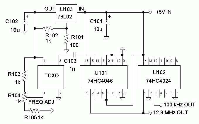
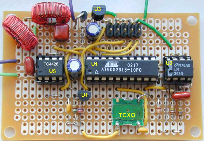
A schematic of the TCXO and the added components is shown in the figure below. The TCXO requires a supply voltage between 2.85 and 3.15 volts. There are some 3-volt regulators in the Digi-Key catalog, but they all seem to be surface mount parts, so I used a 78L02 2.6 volt regulator with resistors R101 and R102 to raise the output voltage to approximately 3.0 volts. As indicated above, U101 and U102 are optional. The output of the TCXO can be connected to the X1 input (pin 5) of the microprocessor, with C103 remaining in the circuit as a DC blocking capacitor. C102, a 10 uF capacitor, is "stolen" from the original exciter board parts list, where it appears as C6. In my board layout, the 220 uF capacitor C13 is located right at the input to the 78L05 regulator, so C6 is not necessary.
TCXO and associated components
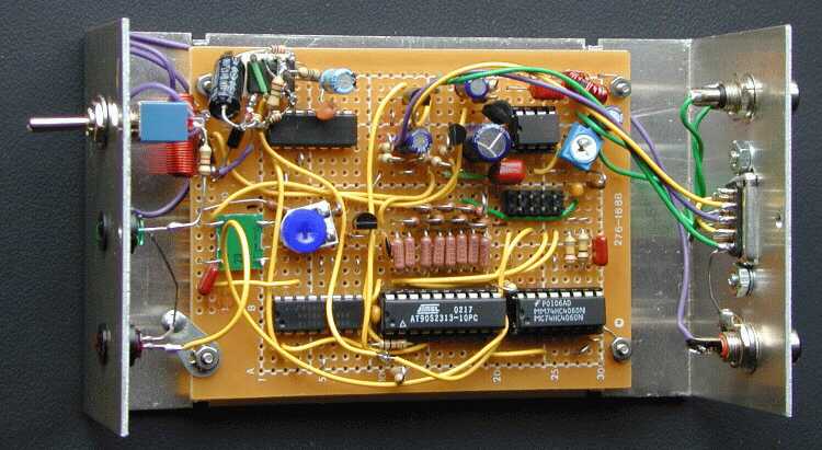
I originally planned to put the TCXO components on a small Radio Shack 276-150 prototype board that would be mounted as a "daughter" board. However, the entire DDS circuit and the TCXO components will fit on a Radio Shack 276-168 prototype board (dimensions approximately 2.8 by 3.25 inches). This makes for a nice compact unit, although the little board gets pretty busy and allows no room for future add-ons. It might be easier to use a more open layout like the one Murray shows in his users guide. The component layout I used is shown in the photograph below. One of the trickiest parts of the construction is to make the connections to the tiny pads on the surface-mount TCXO package. I did it by soldering four bare wires (clipped-off component leads) to the circuit board, positioning the TCXO upside down, and bending the wires down to contact the pads. Then a quick dab with the soldering pencil made the connections. Be sure to keep track of the TCXO pin numbers, and remember that they go clockwise when viewed from the bottom of the package.
The Radio Shack prototyping board is convenient for circuits with DIP packages, because it has groups of 3 connected pads on either side of buses that can be used to route the +5 volt power and ground. This saves a lot of point-to-point wiring. I used the board as is, with one minor modification. The 10-pin programming header has pins 4, 6, 8 and 10 grounded, while pin 2, on the same side of the header, is connected to +5 volts. I used a Dremel tool to cut through the copper traces and isolate a short section of the ground bus where pin 2 of the header is connected. A jumper (the green wire under the programming header) re-establishes the ground bus connection to the left of the header.
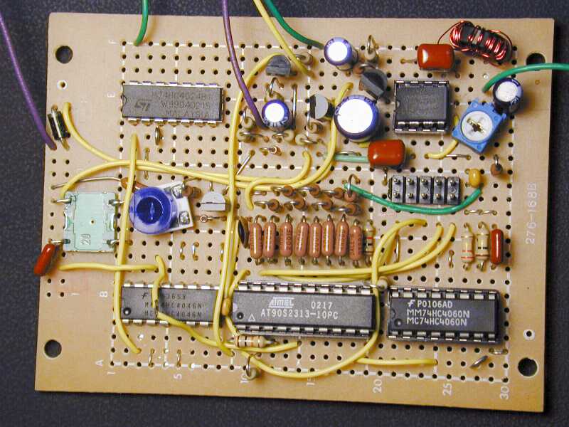
Component layout
I plan to use the DDS exciter primarily to drive an LF final which is remotely located at the base of the antenna. Once the drive level is set, it should not not need to be changed, so I used a board-mounted potentiometer rather than a panel control for the output level adjustment. The TDA7052A output amplifier has a voltage-variable gain adjustment. In Murrays original circuit, the level control is a 1 meg potentiometer from the control pin to ground. I used a 1k potentiometer, with another 1k resistor in series with the 5 volt supply to limit the maximum voltage to 2.5 volts. It takes about 2 volts to set the TDA7052A amplifier to maximum gain.
Another board-mounted potentiometer (R104 in the TCXO schematic above) is used to fine tune the TCXO frequency, which can be adjusted a few ppm in either direction by applying a voltage between 0.5 and 2.5 volts to the control pin. The circuit shown limits the voltage to the range of 1.0 to 2.0 volts. I had no problem setting the TCXO to give a reading of 12.800000 MHz on my frequency counter. With the control pin floating, the TCXO ran about 0.6 Hz low in frequency. Thats less than 0.5 ppm error, so the calibration pot may be needed only for really precise tuning. Actually it isnt needed even then, because the calibration can be corrected in the DDS exciter software. But I like to do things the old-fashioned way.
RF output is taken from the small toroid transformer in the upper right corner of the board. If you plan to use the exciter at very low frequencies, a larger toroid core or even an audio transformer would be advisable. However, even with the FT37-77 core, the response is fairly flat down to 50 kHz and below. I didnt use a tapped transformer; mine is simply a 1:1 transformer with 24 turns of #30 wire on both primary and secondary. A bifilar type of winding is commonly used in broadband transformers and has the advantage that you only have to thread the (doubled) wire through the core 24 times. You dont need to count the turns, just wind it until its full, because 48 turns is about all the little core will hold.
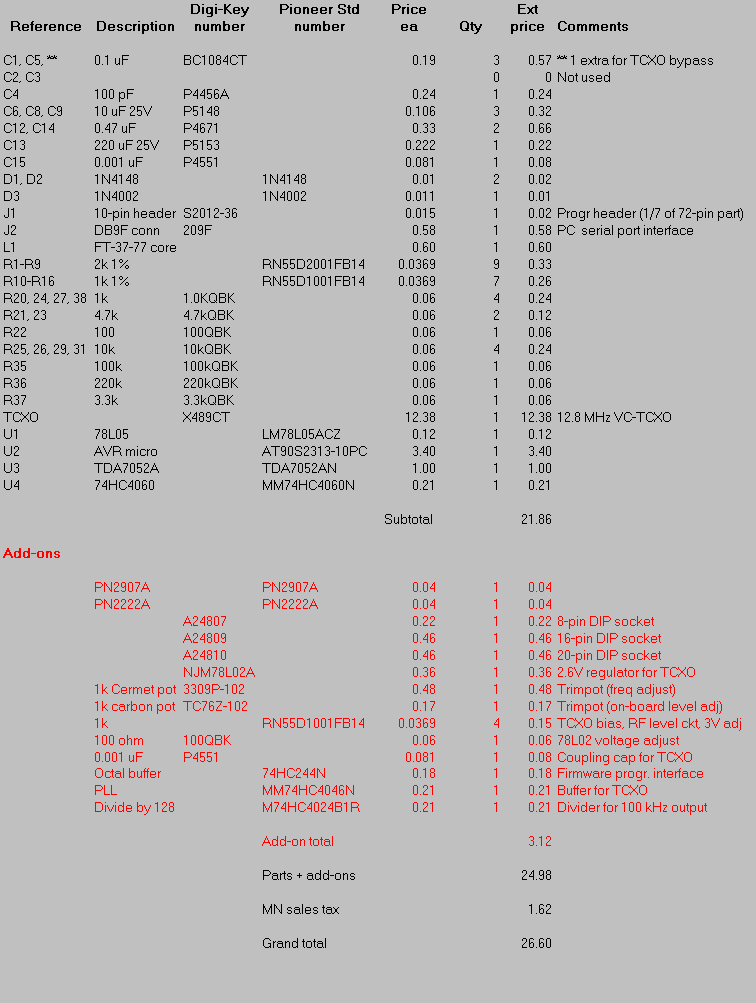
The parts list below includes all of the board-mounted parts, including the optional TCXO buffer and divide by 128 circuit. It does not include the circuit board, case, RF output connector, power connector or LEDs. I did not provide all of the parts for the programming interface, because I planned to pre-program the AVR microprocessors for those who ordered sets of parts from me, and programming is supposed to be a one-time operation. Unfortunately this may not be true, as discussed later.
Prices shown in the parts list are for an order quantity of 10 sets of parts. In most cases, there is little price difference between single lots and lots of 10, although the TCXO in single-unit quantities is a little over $15. It is always a struggle to get all the parts for even the simplest projects from one or two suppliers, and the shipping/handling charges can sometimes exceed the parts cost. In this case, all of the parts except the toroid core were available from two suppliers Digi-Key (www.digikey.com) and Pioneer Standard. I purchased the toroid cores from Bytemark (www.bytemark.com). Note: I learned in March 2003 that Pioneer Standard has sold its component business to Arrow Electronics (http://arrow.com). Supposedly they will recognize the Pioneer Standard part numbers given below, although I can't guarantee that they will be happy about supplying parts in single-unit quantities!
Problems -- Except for a couple of my own wiring errors, the board fired up and performed as expected. There is a minor error on one of the schematics which Murray may have corrected by now. The Vcc pin on U2, the AVR microprocessor, is incorrectly labeled as pin 7. Like most digital ICs, the power and ground pins are at opposite corners of the chip, and the Vcc pin is actually pin 20.
The microprocessor in the DDS exciter seems to be very susceptible to voltage transients. Im not sure how they are getting in, but if I turn other connected equipment on or off, the microprocessor may hang up and the memory (not sure if it is just the EEPROM memory or the program memory as well) can get scrambled. When that happens, it is necessary to re-program the microprocessor. This was happening during bench testing, and I blamed the haywire nature of all the connections. However, it still happened at times with the exciter mounted in a metal box (admittedly, with the box open and with scope leads attached). I added a 0.001 uF capacitor from the reset line of the microprocessor to ground, and also installed a small RF choke in the 12V power lead. After incorporating the reset circuit described below, the exciter has been operating reliably, as long as I don't do anything silly like firing up the HF rig on 75 meters with the programming cable connected.
Memory loss can also occur when the exciter is turned off and back on. This may be happening because the programming pins are in an unknown state during the rise and fall of the supply voltage. I noticed that the exciter did not always come up on the right frequency, and sometimes one or more characters in the message would be mis-sent, so I ran a test to quantify the problem. During this test, the programming cable was plugged into the board, but not the serial cable. After each off/on cycle, I verified the EEPROM contents using the Atmel software, and if necessary, cleared the memory and re-programmed it. When the switch on the exciter box was used to turn power off and on, the EEPROM failed verification about 7 out of 10 times. It didn't seem quite as bad when I switched the 12 volt power supply, but the failure rate was still about 50 per cent. Obviously this had caused a bit of frustration!
Murray confirms that others have observed a memory corruption problem, but obviously not to the extent that I have, and apparently nobody has developed a solid fix for it. I have no way of knowing whether the memory corruption happens as the power is ramping up or when it is ramping down, so I designed a circuit that would hold the reset line of the microprocessor low for a brief period whenever the power is turned on or off. The circuit is more complex than I would like, and Im sure someone can come up with a simpler way of doing the same thing. But the circuit does seem to work. With the reset circuit connected, there were no EEPROM verification failures in 10 off/on cycles with the local switch, and 10 off/on cycles with the power supply switch. At that point I decided to quit while I was ahead. No doubt there are external influences such as keying up my kW amplifier (on HF, that is) that may scramble the EEPROM, but at least it now appears possible to turn off the power without losing the program.
The reset circuit is shown below. In the description of operation, I have assumed a 12 volt supply, but the exciter (and this circuit) will work at other voltages. U301 is an LM393 dual comparator. The more common LM339 quad comparator (available at Radio Shack) should also work if you use the correct pin numbers. (Ground all the pins on the two unused comparators.) R301 through R303 form a voltage divider with taps at 1/3 and 2/3 of the supply voltage. R304 and R305 form another divider that provide a voltage of ½ the supply voltage after C302 is charged. When the 12 volt power is turned on, C302 is discharged and the voltage on pin 3 of U301A is near zero, but the voltage on pin 2 rises almost instantly to about 4 volts. This pulls down the output pin, which is connected to the reset pin (pin 1) of the AVR microprocessor, holding it in the "reset" state. After about half a second, the voltage across C302 rises above 4 volts, and the reset pin is allowed to "float". The outputs of the LM393 are open collector; that is, they look like an open circuit when not pulled low.
When 12 volt power is first removed, C302 is charged to about 6 volts, but the voltage on pin 5 of U301B drops rapidly, again pulling down the microprocessors reset pin. Capacitor C303 maintains power on U301 until the voltage on the remainder of the exciter circuit has dropped to a point where the reset circuit is no longer needed. Note: the "12 volt "connection is made on the power-supply side of diode D3 in Murrays circuit diagram for the exciter.
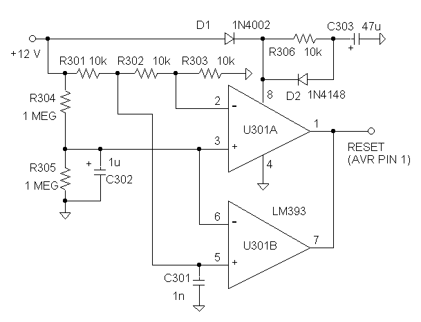
Power-up/power-down reset circuit *
I mounted the 8-pin LM393 comparator IC dead-bug style on a corner of my circuit board, and the associated parts are more or less hanging in space around it. In retrospect, a larger board would indeed have been a good idea.
*Note: I later found that an inexpensive voltage detector IC in a TO-92 package will replace all of the components shown above! Further details are given in the description of the "All in One" DDS exciter.
Programming is a relatively simple task using the Atmel software. But be sure to download version 2.65 as suggested in Murrays users guide, because the current version from the Atmel web site may not work. The parts list above includes the 74HC244 octal buffer that is used in the programming adapter, but does not include the other necessary components. The only part for the adapter that cant be found at Radio Shack is the connector that plugs into the 10-pin programming header on the exciter board. I got the connector and ribbon cable for my homebrew programming adapter from an old IDE card in my junk box. Cables like that were commonly used to connect the serial ports to the IDE board, prior to the time when all of those functions were incorporated into computer motherboards.
At first, programming the exciter to change modes
and send different messages was a humbling process for an old fogey like
me. It took a while to learn the commands and start thinking in hexadecimal.
The KISS mode is preferred, because it allows access to all of the functions
of the exciter. However, it has one disadvantage: a single missed keystroke
means that you have to start all over. Sometimes it is easier to go into
the Atmel software and key the numbers into the EEPROM buffer memory, and
then load them into the device via the programming cable. (This also has
a disadvantage because I didn't mount a connector on the outside of the
box.) Murray explained the organization of the EEPROM contents, and I have
summarized the information (to the extent that I understand it) in the
picture below. The first two bytes in the memory are ignored -- apparently
these are the most susceptible to corruption. Then there are three bytes
to set a default frequency, followed by a default mode and offset, The
8th byte sets the baud rate for communication with the PC via the serial
port. After that there are several bytes that relate to a function that
has not been implemented, so it probably makes no difference what is entered
there. Finally there are some FFs to fill out the first line.
Starting on the second line are the commands to
set up the beacon message. I believe the initialization commands for frequency,
mode, rate and shift can appear in any order. In this example the frequency
is 182.201 kHz and the mode is 1, which is "ASK" (amplitude shift keying,
or plain old on-off keyed CW). I start out with a CW identifier at 12 WPM,
which requires a setting of 0007. No frequency shift is desired, so that
parameter is set to zero. Maybe this command isn't even necessary for mode
1. Then come the hexadecimal representations of the Morse characters in
my CW identifier, based on the table in the user's guide. It happens that
my CW identifier ends on line 2, but the CW message could continue until
the EEPROM memory is full.
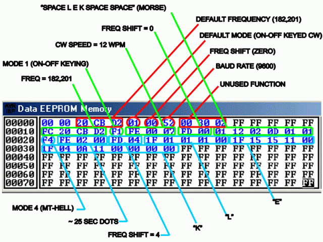
EEPROM contents example
In this case, after the CW identifier is sent, the mode is changed to mode 4 (multi-tone frequency shift keying to provide a graphic "Hellschreiber" display of the letters of the identifier). No new frequency is specified, so the baseline will be the same as the frequency of the CW message. The "dot" length is set to about 25 seconds. At this point I don't know how the timing is defined in mode 4, and the hexadecimal number of 0200 for 25-second dots was arrived at partly by scaling the sample script in the user's guide, and partly by trial and error. The frequency shift is set for 4 steps (approximately 0.4 Hz between rows in the Hellschreiber display). Finally, the hexadecimal character strings for the "LEK" Hellschreiber identifier are entered, with 00s added between each character to provide spacing. The user's guide contains a complete table of Hellschreiber fonts. I found that it wasn't necessary to add a second 00 byte to the one that was already at the end of the string for the "L", and that the "E" looked better when one of the "15" bytes in the table was omitted. This will explain the discrepancies between the EEPROM coding and the font table in the user's guide, for anyone who is patient enough to follow that closely! At the end of the "K" string there are some trailing zeros for spacing, followed by a bunch of FFs. When the program encounters the first FF, it jumps back to the beginning of the beacon message and starts over with the CW identifier.
My exciter is mounted in a 3" X 5.25" X 2.125" box, as shown in the photo below. The reset circuitry is clustered in the upper left corner of the circuit board. I used RCA connectors for both power and RF output connections. With luck I wont plug the connectors into the wrong jacks too many times.
Exciter mounted in enclosure.
The exciter has no problem driving my complementary-pair 1 watt final amplifier, which is remotely located at the base of my antenna. A drive setting of 4 volts p-p is adequate, and although the exciter is capable of more drive, the output from the final doesnt increase once the drive is between 3 and 4 volts p-p. In its initial testing, the exciter has been used to send multi-tone Hellschreiber format using Murrays font table, at dot speeds ranging from a few seconds up to 30 seconds. Reception reports so far have come from a number of states, with Steven Brooks in Arizona currently holding the DX "record" at over 1300 miles. Even though MT-Hell may not have quite the weak signal capability of QRSS30, it certainly stands out on the Argo display.
Hexadecimal conversion spreadsheet
Murray's software will do the necessary decimal to hexadecimal conversions for use when programming in KISS mode or entering data directly into the EEPROM buffer. But I thought it would be convenient to put everything I normally use into a spreadsheet that could be brought up as a separate window. If you have Excel 97 or later, it should be possible to download ZL1BPU-freqcalc.xls and use it for your own calculations. I'm not a power Excel user so this is not a very elegant spreadsheet, but it should be fairly easy to use. The example below is what you should see when you open the file. As indicated, the cells with numbers in red are for user entries; don't mess with the other cells unless you want to change the way the calculations are performed! If your copy of Excel does not have the data analysis toolpack enabled, you need to go to the "Tools" menu, click on "Add-ins", and check the "Analysis toolpack" item. This will enable the DEC2HEX and HEX2DEC functions in Excel.
As can be seen from the example below, there are five different places where you can enter a desired frequency and obtain the corresponding hexadecimal code. That way you can do a new calculation but leave a few of your "favorites" displayed. Entering a frequency in the 5th row (where 185299 appears in this example) will immediately show the next twenty 0.1 Hz (approximately) steps. This might be useful if you want to squeeze in among a group of existing LowFER beacons such as the 185.3 kHz "watering hole".
The spreadsheet will also perform the frequency calibration function if you don't know the exact frequency of your reference oscillator but have a way of checking the output frequency. For example, in the "barebones" version of the exciter to be described later, I used an inexpensive 12 MHz microprocessor crystal. Entering the value of 12000000 for the crystal frequency, I find that an output frequency of 182.201 kHz requires a hexadecimal entry of 22FB8B. But when I look at the Argo screen, I see that my frequency is 12.7 Hz above BRO, who is transmitting on 182.200 with a GPS-disciplined frequency standard. When I entered the desired frequency of 182201 in cell A11, the predicted frequency automatically appeared in the "Crystal calibration" calculation in cell J13. After entering the measured frequency, in this case 1822127 Hz, in cell K13, the spreadsheet says that my actual crystal frequency is 12000771. Now if I type that frequency into cell B4, all of the hexadecimal numbers will be corrected (including the number used to set the baud rate). Note that you can't just copy the calculated crystal frequency from cell L13 and paste it into B4, because Excel will recognize that as a "circular reference". You can do a "paste special" and paste only the value, but it's not that hard to enter the number manually.
By measuring the actual frequency at the test point (pin 7) of the 4060 dot clock generator, you can get the correct hexadecimal values for a desired baud rate, QRSS dot time, or CW speed in WPM. Murray's documentation (if I'm reading it correctly) says that the CW speed in WPM is the baud rate divided by 1.2. I think it's the other way around. Anyway, 12 WPM CW is supposed to have a dot length of 0.1 second, and the speeds sound about right when I use the numbers from this spreadsheet. Note that in the "bare bones" exciter circuit described later, the symbol clock comes directly out of the oscillator and there is no divide-by-four circuit. The actual output frequency of the clock oscillator (nominally 64 Hz) would have to be entered in cell G6.
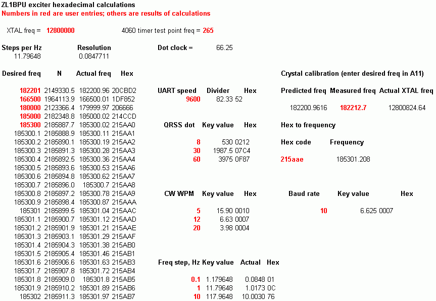
Excel spreadsheet example
After playing with the exciter for a while, I decided that it would be nice to have a second one on hand, so that one is available for experiments on the workbench while the other one is running the beacon message. After all, they can't copy you if you're not on! Since I normally use a fixed level, square wave signal to drive my LF final, I built a "bare bones" version that does not have the R-2R ladder network to provide a sine-wave output, and I replaced the TDA7052A amplifier chip with a complementary-pair output circuit. This is the same output circuit that I have used for years in my LowFER final amplifer, so that with the addition of an output filter, this "exciter" can serve as a complete LowFER transmitter.
"Bare Bones" exciter circuit
The circuit diagram of the Bare Bones exciter doesn't look much simpler than Murray's original version, and in fact it seems more intimidating at first glance. However, everything is on one schematic page here, including a power on/off reset function. There are no hard-to-find components in the circuit, and I believe everything in the diagram can be purchased from a single vendor like Digi-Key. I didn't generate a parts list, because with the exception of the AVR microprocessor, I used components that I already had on hand. A 74HC14 hex inverter provides multiple functions, including the "symbol clock" generator, power on/off reset, level translator for the RXD serial input, and buffer/driver for the complementary pair final. A square-wave output is taken from PB7 (pin 19) on the AVR chip. If you look at this output on a scope, it can be disconcerting because the output is not a constant, 50 per cent duty cycle square wave. But as Murray points out in his user's guide regarding the sine-wave output of the original version, "When you are marvelling at the waveform, remember that all the 256 points do not appear in every sine wave cycle". In other words, it looks like the output is not quite a stable sine wave, and this effect is magnified when only the most significant bit of the output waveform is used. However, my LowFER final amplifier delivers the same field strength with the bare-bones exciter as it does with the sine-wave drive from Murray's original version, and the spectrum on the Argo screen is just as clean. It's also the same as the output obtained with my old exciter, which does deliver a 50 per cent duty cycle square wave. By the way, my final amplifer has a power limiter circuit that restricts the DC input to no more than 1 watt no matter what happens to the drive or the antenna tuning.
"Bare Bones" board layout
As seen in the above photograph, it is
possible to construct the whole circuit on a Radio Shack number 276-150
"general-purpose IC PC board", which is about 1.8 by 2.9 inches overall.
There are even a few holes left over! As with the first version of the
exciter I built, a larger board would have made the layout easier, but
I'm running out of room in the shack. At the left end of the circuit board,
there is a 51 ohm resistor, which is in series with the output coupling
capacitor C11. This resistor does not appear in the schematic, but I added
it to reduce the drive to the remote final amplifier. Although the amplifier
will tolerate a 12 volt p-p drive level, it can get by with considerably
less.
I used an inexpensive 12 MHz microprocessor
crystal in this version of the exciter, although a 12.8 MHz TCXO is a worthwhile
investment at $15. It's nice to know exactly what frequency you're on!
Besides that, a 12.8 MHz reference is desired (perhaps required) for Jason
mode operation. The particular crystal I used seems to be quite stable,
and the output frequency held within +/- 0.1 Hz during an overnight run
with the exciter sitting exposed on the workbench. However, the shack temperature
varied by only a few degrees, and other cheap crystals might have considerably
more drift, so your mileage may vary. If C4, C5 and the crystal are removed,
there's enough room to stick the little TCXO package in the lower right
corner of the board.
Now if you already have a ZL1BPU exciter and want another really bare-bones unit with a fixed beacon message, you can use the original circuit to program the EEPROM, and eliminate the programming header and all of the serial interface components. The resulting self-contained beacon transmitter schematic would be as shown below.
A really bare-bones beacon transmitter.
"All in One" DDS LowFER Transmitter
If you aren't confused enough by all of my adaptations of Murray's design, here is one more. Maybe this will be the last! I'll call it the "All in One" transmitter because it makes my previous circuit by that name obsolete. This circuit incorporates a couple of features that may be of interest even to those who wish to use a separate final amplifier.
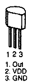
First, and most important, this circuit uses a voltage detector (also known as a "microcontroller supervisor") chip to provide the microprocessor reset function. I found out about these chips (to my chagrin) after building the earlier versions of the exciter. A little 3-terminal device in a TO-92 or surface-mount package replaces all of the components in my earlier reset circuits! Devices with different voltage thresholds and different output configurations are available from suppliers like Digi-Key. For this application, I chose a device (MCP120-475D) with a threshold range of 4.50 to 4.75 volts, and an N-channel open-drain output that is active low. The pinout diagram for the TO-92 package is shown below.
Another thing that is different in this circuit is the use of a power MOSFET driver in place of the complementary-pair final. Several versions of these drivers are available, but for a 1-watt output I chose the TC4426, a dual 1.5 amp driver in an 8-pin DIP package. According to the data sheet, the supply current with no load and a 12 volt supply is only a few milliamps at 200 kHz, and the output impedance per channel is typically 7 ohms. Theoretically this device could make a fairly efficient LowFER final amplifer, and in actual tests it compared favorably to the complementary-pair final. If nothing else, it is easily capable of driving a remote final at the end of a terminated 50-ohm line. The major advantage over the complementary-pair final is a significant reduction in parts count.
As seen in the circuit diagram below, the parts count of the circuit is very low, even though it incorporates the final amplifier and output filter. I used a filter designed for a 50-ohm load and for operation in the LowFER band. Component values can be scaled for use at 136 kHz or for other load impedances. In this version, I used T50-3 (grey) toroid cores for the inductors. Theoretically it takes 60 turns of wire to give 63 uH of inductance. I have trouble keeping track of the turns count, so I simply measured off two 37-inch pieces of #30 enamelled wire and kept the windings as tight as possible. My DMM, which may not be accurate at low inductance levels, says that the coils came out just about right. It all gets ironed out when you tune the antenna, anyway! Larger cores like T80-3 will allow the use of #26 wire and should have somewhat lower losses. I measured an efficiency of about 70 per cent, which is probably within a dB of the best you can expect to do with a simple final amplifier circuit. Note that I didn't provide a means of measuring the final amplifier current separately. Instead, I simply pulled the TC4426 out of the socket and measured the current drain of the rest of the circuit (27 mA in my case) so that it can be subtracted from the total to allow a calculation of the final amplifier input power.
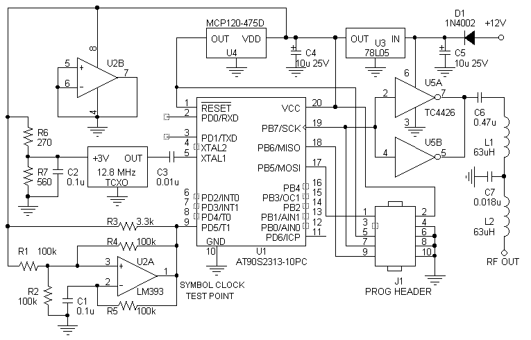
"All in One" DDS transmitter circuit
One half of an LM393 dual comparator is used for the symbol clock oscillator. The other half could serve as the level converter for the RxD line, but I elected not to incorporate the serial interface at all because I find it easier to use the program interface to load the beacon messages. A resistive voltage divider provides the 3 volts for the TCXO, and I chose not to use the voltage trimming pin since the frequency calibration can be done in the software. Of course, an inexpensive crystal oscillator as shown in Murray's original circuit or in the "bare bones" version of the exciter can be used in place of the TCXO if extreme stability is not required.
The complete transmitter, less case and connectors, is shown in the photograph below. Once again, everything will fit on a Radio Shack 276-150 prototyping board. It helps to use 1/8 watt resistors! And if I had to do it over again, I would move the programming header to the right to reduce the congestion in that part of the circuit board.
""All in One" DDS LowFER transmitter layout
Except for the toroid cores for L1 and L2, all of the parts shown in the list below can be purchased from Digi-Key. Where quantities are shown in red, it indicates the minimum quantity in which Digi-Key sells that particular part. I don't usually mind these minimum quantity prices, because the extra parts will be used eventually on another project (or I substitute a part that I already have on hand). You can also beat these prices by shopping around, because at the time of this writing, all of the parts were available from multiple suppliers in the US. For example, Mouser sells TCXOs for a couple of dollars less, and does not usually have minimum quantities on components. Unfortunately the shipping/handling charges usually eat up any savings if you have to split the order among multiple suppliers!
Parts list for "All in One" DDS Transmitter
I hope that by presenting all of these variations, I haven't confused the issue or made the concept look more complicated than it really is. The idea is to provide a number of options so that the individual homebrewer can "mix and match" the portions of the circuit that are suited to his application (and the contents of his junkbox). Whatever version you build, the ZL1BPU exciter is a great project have fun!
DDS Exciter Using the Futurlec AT90S2313 Development Board
Well-known LowFER Dex, (NC, W4DEX) discovered an AT90S2313 development board that is available for under $20 from Futurlec at http://www.futurlec.com/ATDevBoard.shtml Since it uses the same processor as the ZL1BPU exciter, it looked like a possible way to come up with an almost "instant" exciter at a very low cost. I finally got around to ordering one, and have used it successfully to generate QRSS, DFCW and MT-Hell signals to drive my LowFER final amplifier, with the addition of a few inexpensive components on an add-on board.
The photograph below shows a little more detail than the one on the Futurlec site. This is the board as it is was received -- everything in the picture, including the standoffs, came in the package. The overall size of the board is 5.75 by 2.25 inches. As advertised, it has the 90S2313-10PI chip installed. That's the industrial version, which usually costs a bit more than the -10PC part. The crystal is an 8 MHz unit, which is lower than I would like, but it worked just fine in my experiments. There are IC sockets for add-on peripherals such as a real-time clock (including a backup battery holder under the board) and for expansion EEPROM. The board also has a whole array of connectors and headers to communicate with the outside world. Maybe eventually I will acquire some programming knowledge and be able to take advantage of these features, but for now we'll concentrate on the features that the ZL1BPU DDS exciter needs. Basically you need a parallel-port programming header and an optional RS-232 serial interface, plus a way to get at the input/output lines of the microcontroller. No problem; in fact a parallel port programming adapter (with cable) and the MAX232 serial interface chip are included. There is a small prototyping area on one edge of the board. Theoretically you could install a single IC like a 74HC14 hex inverter on the prototyping area to serve as a dot clock generator and a buffer/driver for an LF final, and you'd be ready to go. However, I decided to leave the board in its pristine state and put the additional components on a separate board.
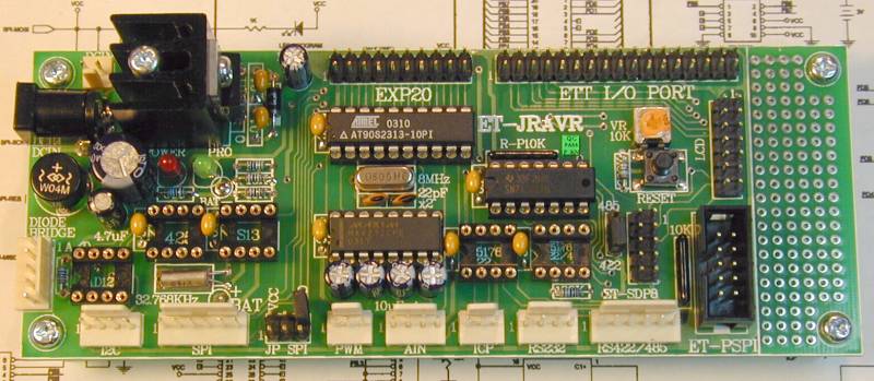
Futurelec AT90S2313 Development Board
Although the development board itself appears to be of good quality and a very versatile tool, the documentation that came with it leaves a lot to be desired. There is no printed manual; everything came on a CD. That's fine with me, but with so much available space on the CD they could at least have provided a more readable schematic. Perhaps they didn't do that because the schematic is incomplete and not accurate anyway. The programming software that comes on the CD does not appear to be usable for this application, and there are no details on how to make the parallel programming interface work. However, there is nothing wrong with the board itself, and in this writeup I will attempt to present all the information needed to get it up and running.
As mentioned before, the schematic, both in pdf format and as a jpg file, is difficult to read and contains some errors. For example, the 4-pin header for the RS232 connection is shown with pin 4 as Vcc and pin 1 as ground. It's actually the other way around. I used the 34-pin expansion header to make connections to the daughterboard on which I mounted the 74HC14 clock oscillator/buffer. The power, ground, and PBx data lines are shown correctly in the supplied schematic, but the PDx port connections are not. I haven't checked out the 20-pin header for accuracy, since I had some old floppy drive cables in my junkbox, and that was a convenient source for the 34-pin connector and cable. If you need to make up your own cable, it would be easier to use the 20-pin expansion port. Futurlec's on-line catalog does not list the 34-pin connectors but they do have the 20-pin version. Don't forget to order the pins along with the connector bodies! For those who want to use the 34-pin header, I have included a readable and correct (I hope) diagram of the expansion port below.
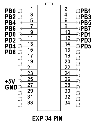
34-pin Expansion Port Header Diagram
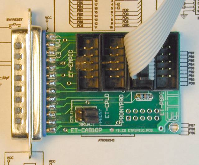
There are four connectors on the programming interface, but there is no mention in the documentation of which one to use. One connector is labeled ET-PSPI; the same as the connector on the development board, and that's the first one I tried. It does in fact work with the programming software on the CD-ROM. Unfortunately, as far as I can tell, that software loads only the "device firmware" (the flash EEPROM) and not the on-chip EEPROM that contains the message memory, default frequency, RS-232 baud rate, etc. It also has no utility for viewing and editing the EEPROM contents. I searched the Web and found a variety of AVR programming software, none of which seemed to work with the supplied interface. I finally determined by trial and error that if you plug the programming cable into the connector labeled PRONYPRO on the interface board and set the two jumpers to the PRONY position, the cable will work with the Atmel ISP software that I had been using with Murray's cable. I assume that the label is supposed to say "PONYPROG", one of the popular chip programmers I ran across during my search. As a clarification, the connector label is offset -- you need to use the connector adjacent to the ET-PSPI connector; that is, the third one away from the DB25 end of the interface board. The photo below shows where to set the jumpers and plug in the cable.
Programming Interface
The AVR ISP v2.65 programming software does not seem to be available on the Atmel web site any more, but I did find this site http://www.paladino.ch/paladino_technical.htm where it is listed as a file called avrtools.zip. The information that is in Murray's documentation and elsewhere in this article applies to the v2.65 software, and the same procedures are followed for programming the development board.
To program the chip on the development board, you follow the same procedures as for other versions of the DDS exciter. You will need to load both Murray's firmware (EXC_D5A.HEX, or perhaps he has a "B" version available now) AND an EEPROM file into the chip before it will start putting out a signal. If you load the .HEX file into the AVR ISP software's program buffer and an EEPROM file into the EEPROM buffer, and then program the device and the EEPROM, theoretically the exciter should start chugging away. However, here is one place where the development board with its supplied programming cable behaves differently from the other versions of the DDS exciter. Previously, I have used Murray's suggested programming adapter, which has a tri-state buffer. That cable can be left plugged in while the exciter is working. With the development board, as long as the programming cable is plugged into the board (and the computer), the microcontroller's reset line is held low. It is necessary to unplug the programming cable before anything will happen. Then you should see activity on the output lines of the microprocessor.
With no "dot clock" supplied to PD5 (pin 9 of the micro), the chip will just sit there and put out the default frequency that is contained on the first line of the EEPROM memory. You can monitor the signal on the MSB of the output -- pin 19 of the micro. There will be a lot of jitter in the waveform and a number of frequency components are present, but a counter will display the correct frequency and you should be able to hear it in a receiver. Note that the hex code for the frequency and UART rate will be considerably different than the examples given earlier in this article, if you are using the 8 MHz crystal that comes on the board. When I first tested the development board, I fed the signal from pin 19 into a 74HC14 hex buffer that drove the coax going out to my final. Two sections of the buffer were connected in parallel, and I put a 51 ohm resistor in series with the coax. There was a horrible looking waveform on the coax, but the final output was essentially the same as with a "clean" drive signal. I used two other sections of the 74HC14 to provide the dot clock signal, and LEK showed up on screen captures from W3EEE and W3NF. The exciter obviously works!
Although it apparently makes little difference because a LowFER antenna acts as a narrowband filter, I prefer to have a somewhat "cleaner" signal going out to my 1-watt final amplifier. If I were running a high-power Part 5 transmitter, I would definitely want to make sure that there are no serious spurious outputs. So after the first night's testing, I used a somewhat more elaborate circuit between the development board and the coax. Essentially I went back to Murray's original idea with the R-2R ladder network acting as a D/A converter, and followed that by a one-transistor active lowpass filter and a 74HC14 buffer. The complete circuit and a photograph of my "daughterboard" are shown below. I built the daughterboard on a Radio Shack 276-168B general purpose prototyping board with the ribbon cable connected in the middle. So far, everything has been squeezed onto one half of the board to leave the other half open for afterthoughts or other experiments. Some day I may try an 8-bit D/A converter in place of the R-2R network, although the simple resistor network seems to do a very good job. Remember that the resistors in the R-2R network must be 1 per cent. None of the other component tolerances are critical. At 185 kHz, the output of the low-pass filter (at the test point labeled TP1) is a pretty clean-looking sine wave. Then I mess it up by running it into a section of the 74HC14 that turns it back into a square wave, but without the jitter seen on pin 19 of the micro. Three sections of the 74HC14 connected in parallel drive the coax going out to the final amplifier in my garage. Two remaining sections of the 74HC14 serve as the dot clock oscillator that puts out a square wave at about 64 Hz. Both of the expansion headers on the development board already have +5V and ground connections, but I wanted to bring in a 12 volt connection to power the active low-pass filter. To do that, I ran a wire on the bottom of the development board between an unused pin on the expansion header and the input pin of the 5 volt regulator (which is also connected by a trace on the board to the + pin on the diode bridge). This is the only modification that I have made to the development board itself.
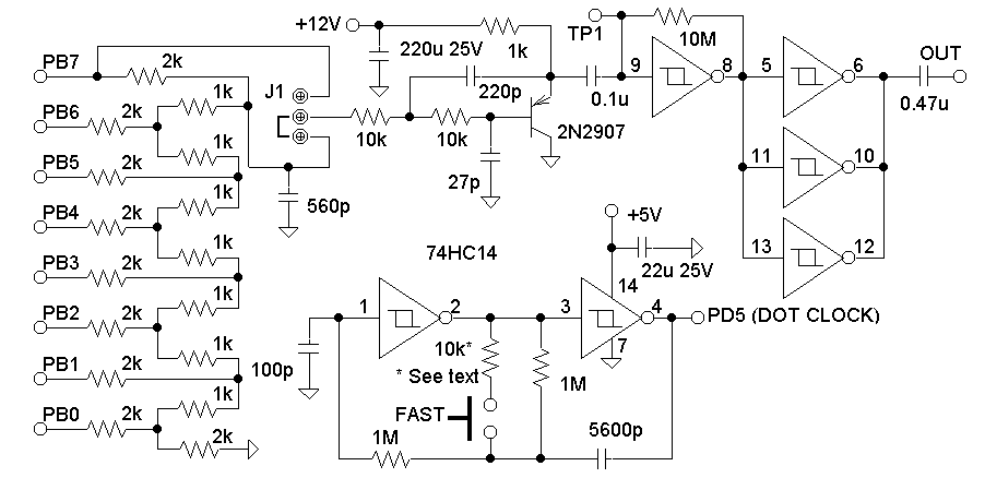
Daughterboard Circuit

Daughterboard Layout
For experimental purposes, I installed a jumper so that the input to the low-pass filter can be connected either to the output of the R-2R ladder network or directly to pin 19 of the microcontroller. It does make a significant difference in the waveform at TP1. It would have been considerably easier to use two ribbon cable connectors and another 34-pin board header than to strip all of the wires in the ribbon cable and solder them to the board. However, that requires a circuit board with side-by side rows of isolated pins with 0.1 inch spacings, and I didn't have one on hand. You may also wonder why I ran wire jumpers between the R-2R network and the pads to which the ribbon cable is connected. When using the R-2R network on the output ports of the microcontroller, which also serve as programming ports, it is necessary to unplug the daughterboard cable during programming. Otherwise the AVR ISP software says that it can't find the device. Apparently the resistors are pulling down one or more lines that are supposed to be high. However, Murray's programming interface works with the R-2R network in place, so I'm not exactly sure what the problem is. The moral of this story is: don't hard-wire the resistors to the output ports -- use something that can be unplugged! If I decide to break the connections to the resistor network at some time in the future (at least to PB5, PB6 and PB7, which are used for programming), it will be easy to cut the jumpers. Anyway, it seemed like a good idea at the time. Probably a better solution is to put a 10-pin header on the prototyping portion of the development board itself, and wire it so that it can be used with Murray's programming cable, which I already have. Then the board can be programmed and the operation of the exciter can be verified without going through the process of plugging and unplugging two cables.
The DDS exciter, in all the versions I've tried, may do unexplained things when it is powered up, like putting out a carrier on a strange frequency for a while. Starting the message with a normal-speed CW identifier, as opposed to a very slow-speed mode, seems to help to shorten the initialization time. I've also seen the first MT-Hell character get messed up, but once things settle down it works beautifully. Just don't get too concerned if something weird happens initially when you power up the exciter. In the circuit diagram of the daughterboard, I have added a "fast forward" button that speeds up the dot clock generator and gets through the process more quickly. This also provides a fast way of verifying that QRSS messages have been programmed correctly, which can otherwise be a very time-consuming process. On the circuit diagram I show a 10k resistor that gets switched in parallel with the 1 meg resistor when the button is pushed, speeding up the clock by a factor of about 100. That's too fast to verify anything other than the QRSS mode. In order to see it, you have to speed up Argo, Spectran, or whatever spectrogram software you are using to view the signal, and in the process you lose the frequency resolution necessary to view modes like DFCW and MT-Hell. For those modes, perhaps a 100k resistor in place of the 10k in my circuit would be appropriate. You could also switch in a trimpot to provide a variable speed-up factor, or simply use a 1 meg pot in place of the fixed resistor to provide a variable-speed clock. Then you could change QRSS speeds without re-programming the exciter.
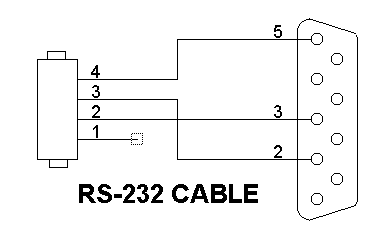
After I had ordered the development board, I found a serial interface cable on the Futurlec site under the "development board accessories" category. $2.50 doesn't sound like a bad price, but the description says that it plugs into a 5-pin connector, whereas the RS-232 connector on the 90S2313 development board has only 4 pins. Hmmm. Anyway, I made my own cable with parts that I had on hand. Futurlec has what look like the necessary connectors in their listing -- a DB9 female connector and a polarized 4-pin connector (part number POLHDCON4, which requires PLHDPIN pins). A connection diagram of the serial port interface cable I made is shown below. Since most of my operation has involved beacon messages which don't get changed very often, I simply program the messages via the parallel port interface and don't even need the serial connection. However, it doesn't cost much to add the serial port capability -- just the price of two connectors and some wire! In order for the serial interface to work, the UART rate in the 8th position on the first line of the EEPROM memory must be set to the appropriate value for the clock frequency. With the "stock" 8 MHz crystal in the exciter, the correct value for a UART baud rate of 9600 is 33 (hex).
Other tidbits that I probably forgot to mention:
The coaxial DC power jack on the development board accepts a 5.5mm X 2.5mm plug. Radio Shack's part number is 274-1573A. You can also feed in power via a 2-pin polarized header. I believe the Futurlec part number for the mating connector is POLHDCON2, which costs considerably less than the coaxial plug -- even though you have to buy the connector pins separately in a package of 10.
Futurlec has a variety of other components including resistors, capacitors, ICs and connectors, plus prototyping boards and plastic cases. It should be possible to get just about everything needed for this project from them. They list the 1k ohm 1 per cent resistors needed for the R-2R network, but they don't seem to have any 2k resistors. At 2 cents each, I guess it wouldn't be a budget buster to put two 1k resistors in series. Futurlec's prices are lower on most items than those of other suppliers, and their shipping charges are very reasonable. My order had a lot of items besides the development board and took over three weeks to get here. However, I have heard from other LowFERs who have gotten much faster service from them.
Frequency stability of the stock 8 MHz crystal is not exceptional but should be adequate, even for modes like QRSS. I observed a drift of 0.2 to 0.3 Hz when the temperature in the shack changed by about 10 degrees F. A 12.8 MHz TCXO or a PTC thermistor attached to the crystal can would provide a more stable signal. Using the 8 MHz crystal offers one advantage -- the smallest frequency resolution is approximately 0.053 Hz, as opposed to 0.085 Hz with a 12.8 MHz clock. The upper frequency limit is not as high, but the circuit performs well up to 200 kHz.
The development board (and daughterboard) can run on supply voltages from 9 to 12 volts DC, and I'm sure you could use a standard 13.8 volt supply with no problem. There is even a diode bridge in the power circuit that should protect against power supply reversal; in fact you could probably run the thing from an AC supply. Current drain of the development board itself is about 37 milliamps. The daughterboard takes another 30 mA or so, depending on how heavily the 74HC14 buffer is loaded.
As with all other versions of the DDS exciter, one nice feature is that the output frequency can be set to anything from the audio range to 200 kHz or more. This offers many possibilities for calibration against precise frequency sources like WWVB or a TV horizontal oscillator signal. And even if you don't have a stable receiver to use for checkout, you can set the output frequency to the audio range and verify your transmission format with audio spectrogram software such as Argo, Spectran or Spectrum Lab.
If you are starting from scratch, this is probably the easiest way to get "on the air" with a DDS exciter. Most of the circuit functions are performed by a $20 pre-wired board. And if, unlike me, you have some programming knowledge, there is an almost endless variety of expansion possibilities!