Solid State Circuits 8 -

3. This circuit provides relatively simple AM detection using a diode detector followed by a solid state amplifier with a positive going AGC output with time constants for AM, CW and SSB. If the circuit is to be used for broadcast reception as well as speech only communications then the AM time constant may need to be increased to prevent bass audio frequencies from affecting the AGC -
The gain of the two transistor AGC DC amplifier on the right hand side of the circuit is determined by the 82R and 5K6 resistors.
The AF stage connected to the AF Output should have a high input impedance compared to the 5K6 RF filter resistor to avoid attenuation of the audio signal.
The two BC214 devices could be replaced by a rail to rail CMOS op-
This page contains a series of AM detectors, showing in addition how a control voltage for an AGC system may be obtained.
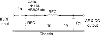
1. A basic detector using a single diode. The OA47 and OA90 germanium diodes will give the best sensitivity as they have the lowest conduction threshold of approximately 100mV but the worst temperature stability. The conduction threshold of silicon diodes like the 1N4148 is about 700mV and Schottky diodes like the HP2805 is about 400mV.
This can be overcome by forward biasing the diode as shown in some of the following circuits but the bias should be temperature compensated using the same type of semiconductor.
The diode must see DC continuity to ground otherwise it will not work correctly. The time constant of the load seen by the diode must be shorter than the period of the highest audio frequency otherwise distortion will occur. The DC output may be used, after filtering, to feed an AGC circuit.
The classic crystal set is based on this type of detector -
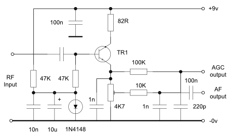
2. The infinite impedance detector was often used in the days of valves as an AM detector and a semiconductor version is shown below. The conduction threshold of the base emitter silicon diode is overcome using a forward biased silicon diode to provide a temperature compensated bias supply.
One slight disadvantage of this circuit is that it has a tendency to oscillate at high frequencies which can usually be cured by inserting a low value resistor, say 22R or 47R, in series with the base connection and/or increasing the 1n emitter capacitor a little.
The BC109 (Ft=150MHz) will be fine up to a few MHz but will need to be replaced with a suitable RF device for higher frequencies. A BF199 (Ft=550MHz) gives a flat frequency response to well above 50MHz but being a low current gain device may require the 47K resistor driving the 1N4148 to be reduced to 22K.
The base emitter diode of TR1 has a reverse breakdown voltage of about 5v so do not overdrive the circuit.
4. The following circuit uses the same detector as in (3) above but with a more flexible AGC arrangement. Rail to rail output CMOS op-
The gain of each op-
The minimum AGC rise time for all modes is set by the 470K resistor and capacitor C1. On AM the rise and fall times are set by the 470K resistor and the 100n capacitor and should be just sufficient to prevent low audio frequencies from affecting the AGC voltage. The AGC fall times on CW/SSB are set by the 4M7 resistor and the 1u or 100n capacitors sepending on the switch position. A ‘Hang’ facility has not been implemented but could be provided with some additional components.
The non-
The circuit around IC1 could be reconfigured to avoid the voltage drop across diode D4.

5. A version 2 example PCB layout may be downloaded from here which includes:
- a semiconductor version of an infinite impedance detector (shown in item 2 above) using a BF199 and with audio and positive going AGC outputs
- a product detector based on an NE602 mixer followed by a CA3140 op-
amp - see here for a similar circuit.
A 9v stable and hum free DC supply for both detectors and about 200mV pk-
The board has been deliberately made small to fit into an existing project but could be larger if that is more convenient or easier for the constructor. Screening may be required around this module to prevent the BFO signal leaking into the adjacent IF module.
The NE602 has a limited dynamic range so a good AGC system is required to prevent any signal overloading.
6. Product Detector
A very simple product detector for SSB/CW may be constructed using a variation of the MOSFET mixer shown here by replacing the collector tuned transformer T2 with a 1K resistor, 1n RF decoupling capacitor to ground and increasing the value of the other decoupling capacitors to cater for audio frequencies. The BFO injection to gate 2 will be about 4v peak to peak so screening may be required to prevent pickup by the early IF stages.