
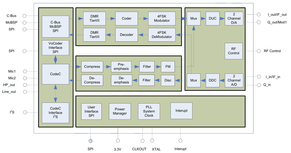
Figure 1
HR_C5000 is Hong Rui independent research and development in line with ETSI TS102 361 (DMR) standard digital intercom dedicated chip.
Chip using 4FSK modulation and demodulation technology, 12.5K channel using 2-slot TDMA communication mechanism to achieve 2
Way digital voice and data communication transmission, support full-duplex, half-duplex communication.
Chip design uses the physical layer, data link layer and call control layer layered design, independent open user interface, fully open
Put the state information and configure the interface, user-depth development of the second to support the agreement parameter configuration, suitable for digital intercom
Handsets, private cluster terminals and low-speed data, voice transmission terminal applications,
support for trunk and end-to-end use.
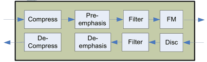
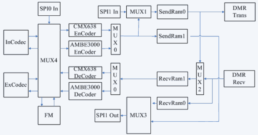
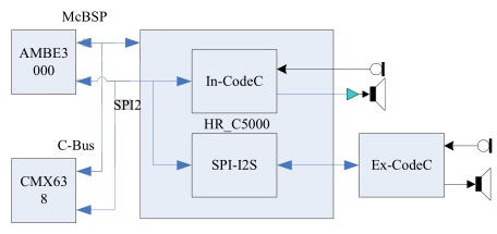
Chip using C-Bus and McBSP interface seamless docking CMX638, AMBE3000 other vocoder chip, while mentioning
For standard SPI interface, flexible selection of vocoder, support for encrypted voice, data interface, while digital voice recording, playback
And a tone input providing interface.
Built-in CodeC, Mic input and Line output, providing Mic gain control and LineOut volume control, there are
Effectively reduces user peripherals and configures standard I 2 S interfaces for external CodeC.
Chip built-in high-performance dual-channel AD / DA unit to support baseband IQ, can be configured IF IQ, can be configured IF and two
Point modulation and other RF interfaces to provide independent IQ bias voltage adjustable design, IQ Road, you can set the cepstrum.
Using standard analog walkie-talkie processing unit to support 12.5KHz / 25KHz channel communication.
3.3V power supply chip, built-in power management module, to achieve low-power design.
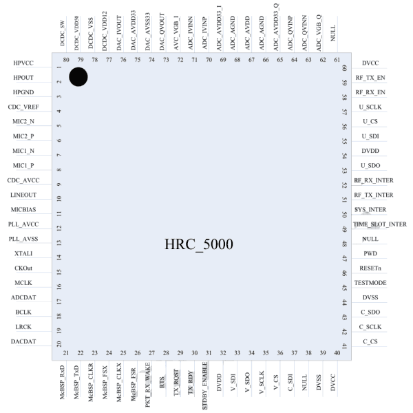
The product is available in 80-pin LQFP or VQFN packages.
| Pin | Name | Category | Description |
| 1 | HPVCC | AI | HP power supply 3.3 V |
| 2 | HPOUT | AO | HP output (n.c. in MD380) |
| 3 | HPGND | AI | HP output |
| 4 | CDC_VREF | AI | HP output |
| 5 | MIC2_N | AI | Mic2 input N |
| 6 | MIC2_P | AI | Mic2 input P |
| 7 | MIC1_N | AI | Mic1 input N |
| 8 | MIC1_P | AI | Mic1 input P |
| 9 | CDC_AVCC | AI | Codec analog power supply, 3.3 V |
| 10 | LINEOUT | AO | Line out (MD380: via PA to speaker) |
| 11 | MICBIAS | AO | Mic bias voltage (MD380: just a C to GND?) |
| 12,13 | .. | .. | supply voltages and GND |
| 14 | XTAL | DI | Clock input (MD380: 29.4912 MHz, X201) |
| 15 | CKOut | DO | Clock output (MD380: n.c.(?) ) |
| 16 | MCLK | DI | CodeC clock input (MD380: n.c.(?) ) |
| .. | .. | .. | .. |
| 21 | McBSP_RxD | DO | AMBE3000 Interface (CMX638: C_CDATA) |
| 22 | McBSP_TxD | DI | AMBE3000 Interface |
| 23 | McBSP_CLKR | DO | AMBE3000 Interface |
| 24 | McBSP_FSX | DI | AMBE3000 Interface |
| 25 | McBSP_CLKX | DI | AMBE3000 Interface |
| 26 | McBSP_FSR | DO | AMBE3000 Interface |
| 27 | PKT_RX_WAKE | DO | AMBE3000 Interface |
| 28 | RTS | DI | AMBE3000 Interface |
| 29 | TX_RQST | DO | AMBE3000 Interface |
| 30 | TX_RDY | DI | AMBE3000 Interface |
| 31 | STDBY_ENABLE | DO | AMBE3000 Interface |
| .. | .. | .. | .. |
| 41 | C_CS | DO | CodeC interface with vocoder SPI2 |
| 42 | C_SCLK | DO | CodeC interface with vocoder SPI2 |
| 43 | C_SDO | DO | CodeC interface with vocoder SPI2 |
| 44 | DVSS | AI | Digital ground |
| 45 | TESTMODE | DI | Test mode |
| 46 | RESETn | DI | Reset |
| 47 | PWD | DI | Sleep (Power Down?) |
| .. | .. | .. | .. |
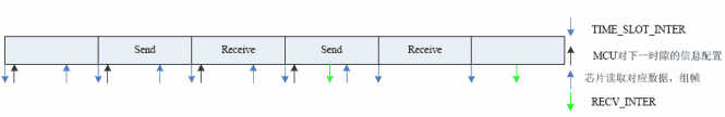
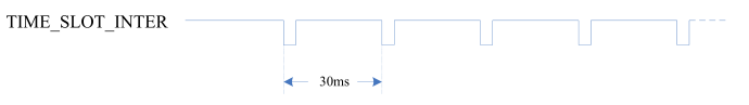
| 49 | TIME_SLOT_INTER | DO | 30ms interrupt |
| 50 | SYS_INTER | DO | System interrupt |
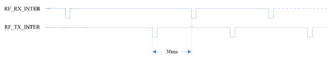
| 51 | RF_TX_INTER | DO | RF transmission interrupt |
| 52 | RF_RX_INTER | DO | RF receiving terminal |
| 53(HR-DS) / 55(MD380) ?? | U_SDO | DO | User Interface SPI0 (serial data out) |
| 54 | DVDD | AI | Digital power supply 1.2V |
| 55(HR-DS) / 56(MD380) ?? | U_SDI | DI | User Interface SPI0 (serial data in) |
| 56(HR-DS) / 58(MD380) ?? | U_CS | DI | User Interface SPI0 (chip select in) |
| 57(HR-DS, MD380) | U_SCLK | DI | User Interface SPI0 (serial clock in) |
| 58 | RF_RX_EN | DO | RF receive channel open signal |
| 59 | RF_TX_EN | DO | RF transmit channel open signal |
| .. | .. | .. | .. |
| 73 | DAC_QVOUT | AO | Q-channel DAC output (IF Q-path / baseband Q-path / IF / two points) |
| 74 | DAC_AVSS33 | AI | DAC Analog Ground |
| 75 | DAC_AVDD33 | AI | DAC power supply 3.3V |
| 76 | DAC_IVOUT | AO | I-channel DAC output (IF I-path / baseband I-path / IF / two points) |
| .. | .. | .. | .. |
| 80 | DCDC_SW | AO | DC-DC switching output |
| Type | Address | Read/ Write |
Name | Default Value |
Definition | Description |
| Reset | 0x00 | W | DMRnRst PHYnRst CodecRst FMnRst VocoderRst UDCDDCRst IISRst CoderCRst | 0x00 | Bit7 Bit6 Bit5 Bit4 Bit3 Bit2 Bit1 Bit0 |
0 DMR protocol reset 0 Physical layer reset 0 Codec reset ... ... ... ... ... |
| Hardware Config | 0x01 | W/R | RFTransIQMode RFRecvIQMode RFTransMode RFRecvMode Bit1HasNoName Bit0HasNoName | 0x14 | Bit 7 Bit 6 Bits 5..4 Bits 3..2 Bit 1 Bit 0 |
0 for IQ, 1 for QI 0 for IQ, 1 for QI 00 = TX intermediate frequency mode 01 = TX intermediate frequency IQ mode 10 = TX baseband IQ mode 11 = "two-point modulation mode" (?) 00 = RX intermediate frequency mode 01 = RX intermediate frequency IQ mode 10 = RX baseband IQ mode 11 : not specified in the datasheet I/Q balancing: 1=on, 0=off (??) reserved |
| 0x02 | W/R | TransIsigCenter | 0x00 | Bits 7..0 | Bias value for TX, I-channel | |
| 0x03 | W/R | RecvIsigCenter | 0x00 | Bits 7..0 | Bias value for RX, I-channel | |
| 0x04 | W/R | TransQsigCenter | 0x00 | Bits 7..0 | Bias value for TX, Q-channel | |
| 0x05 | W/R | RecvQsigCenter | 0x00 | Bits 7..0 | Bias value for RX, Q-channel | |
| 0x06 | W/R | Vocoder- and SPI selection | 0x40 | .. | see table 12 in chapter 8 | |
| 0x07 | W/R | IFFreq2 | 0x0B | Bits 7..0 | IF frequency, upper 8 bits | |
| 0x08 | W/R | IFFreq1 | 0xD9 | Bits 7..0 | IF frequency, middle 8 bits | |
| 0x09 | W/R | IFFreq0 | 0x54 | Bits 7..0 | IF frequency, lower 8 bits | |
| 0x0A | W/R | CLKOutDiv | 0x02 | Bits 7..0 | External clock output freq | |
| 0x0B | W/R | PLLM | 0x0A | Bits 7..0 | PLL M register | |
| 0x0C | W/R | PLLBP PLL Sleep PLLDO PLLN | 0x82 | Bit 7 Bit 6 Bits 5..4 Bits 3..0 |
0=in use, 1=bypass 0=normal operation, 1=sleep PLL output divider PLL input divider (see note in chapter 6) | |
| 0x0D | W/R | Codec Ctrl Suspend Sleep Switch2 AntiPop | 0xC8 | Bit 7 Bit 6 Bit 5 Bit 4 Bit 3 Bits 2..0 |
Codec Ctrl: details further below Suspend: details further below Sleep: details further below Switch2: details further below AntiPop: details further below reserved | |
| 0x0E | W/R | HPoutEn HPMute HPOutVol LineOutEn Mic1En Mic2En Switch1 | 0x00 | Bit 7 Bit 6 Bits 5..4 Bit 3 Bit 2 Bit 1 Bit 0 |
HP output enable 0=off,1=on 1: HP output muted 00=0dB...11=6dB Line Out enable: 0=off, 1=on Mic1 enable: 0=off, 1=on Mic2 enable: 0=off, 1=on Switch1 (?) : 0=off, 1=on | |
| 0x0F | W/R | ADLinVol | 0xB8 | Bits 7..3 | 11101: 9 dB .. 00000: -34.5 dB MD380: Modifying bits 7..3 during transmit affects the volume of DTMF tones and the voice signal, depending on reg 0x0E. Details further below. | |
| 0x0F | W/R | MicVol | Bits 2..1 | 00: 0 dB 01: 6 dB 10: 12 dB 11: 20 dB | ||
| Parameter Config | 0x10 | W/R | ModulatorMode TierMode ContinueMode LayerMode ISRepeater ISAligned RepeaterSlot | 0x30 | Bit 7 Bit 6 Bit 5 Bits 4..3 Bit 2 Bit 1 Bit 0 |
0 for DMR, 1 for FM 0 for Tier1, 1 for Tier2 0 = Continue, 1 = TimeSlot 00=phys. layer, 01=?table?, 10=Layer 2 0 for non-relay, 1 for relay 0 for offset, 1 for alignment 0 indicates Slot1, 1 indicates Slot2 |
| 0x11 | W/R | LocalChanMode | 0x80 | Bit 7 Bit 6 Bit 5 Bit 4 Bit 3 Bit 2 Bit 1 Bit 0 |
'Repeated'/'Direct' simplex(?) 'Repeated'/'Direct' duplex(?) 'Repeated'/'Direct' simplex with RC'(?) 'MStoFixedDuplex' (?) 'SingleFreqSimplex' (?) 'EmbeddedOutboundRC' (?) 'DedicatedOutboundRC' (?) reserved | |
| 0x12, 0x13 | don't exist ? | |||||
| 0x14 | W/R | LocalSrcAddrL | 0x01 | .. | .. | |
| 0x15 | W/R | LocalSrcAddrM | 0x00 | .. | .. | |
| 0x16 | W/R | LocalSrcAddrH | 0x00 | .. | .. | |
| 0x17 | W/R | LocalGroupAddrL | 0x01 | .. | .. | |
| 0x18 | W/R | LocalGroupAddrM | 0x00 | .. | .. | |
| 0x19 | W/R | LocalGroupAddrH | 0x00 | .. | .. | |
| 0x1A | W/R | LocalBSAddrL | 0x01 | .. | .. | |
| 0x1B | W/R | LocalBSAddrM | 0x00 | .. | .. | |
| 0x1C | W/R | LocalBSAddrH | 0x00 | .. | .. | |
| 0x1D | W/R | LocalUnAddrL MaskUnaddr | 0x00 | .. | .. | |
| 0x1E | W/R | LocalBroadcast MaskBroadcast | 0x00 | .. | .. | |
| 0x1F | W/R | LocalEMB | 0x10 | .. | .. | |
| 0x20 | W/R | LocalAccessPolicy | 0xAA | .. | .. | |
| 0x21 | W/R | LocalAccessPolicy1 | 0xA0 | .. | .. | |
| 0x22 | W/R | EncodeStart EncodeStop DecodeStart DecodeStop | 0x00 | Bit 7 Bit 6 Bit 5 Bit 4 Bits 3..0 |
1 = vocoder encoding begins 1 = end of vocoding 1 = vocoder decoding begins 1 = vocoder has finished decoding reserved | |
| 0x23 ..0x2F | not specified in the datasheet | |||||
| External Codec | 0x30 | W/R | BCLK_CNT_H | 0x00 | Bits 7..0 | Mclk / BCLK division ratio, upper 8 bit. See Chapter 10, External Codec Clock |
| 0x31 | W/R | BCLK_CNT_L | 0x00 | Bits 7..0 | Mclk / BCLK division ratio, lower 8 bit | |
| 0x32 | W/R | LRCK_CNT_H | 0x00 | Bits 7..0 | Mclk / LRLK division ratio, upper 8 bit | |
| 0x33 | W/R | LRCK_CNT_L | 0x00 | Bits 7..0 | Mclk / LRLK division ratio, lower 8 bit | |
| FM | 0x34 | W/R | FMBpfOn FMCompressorOn FmPreEmphasisOn FmBandWidth | 0xF0 | Bit 7 Bit 6 Bit 5 Bit 4 |
0 = band-pass filter off, 1 = on 0 = compression off, 1 = on 0 = pre-emphasis off, 1 = on 0 = 12.5 kHz, 1= 25 kHz |
| 0x35 | W/R | FM_dev_coef | 0xA0 | Bits 7..4 Bits 3..0 |
FM modulation factor reserved | |
| RSSI | 0x43 | R | RSSILevelH | 0x00 | detected RSSI level, upper 8 bits | |
| 0x44 | R | RSSILevelL | 0x00 | detected RSSI level, lower 8 bits | ||
| DLL (Data Link Layer) | 0x50 | W/R | LocalDataType | 0x00 | Bits 7..4 Bit 3 Bit 2 Bits 1..0 |
TX time slots DataType or A ~ F 0 = data, 1 = voice reserved LCSS for each transmit time slot |
| 0x51 | R | DLLRecvDataType DLLRecvPI DLLRecvCRC SyncClass | 0x00 | Bits 7..4 Bit 3 Bit 2 Bits 1..0 |
received data type received PI 0=received data check ok, 1=error 00=no sync hdr, 01=voice, 10=data,11=table RC | |
| 0x52 | R | DLLCC | 0x00 | Bits 7..4 Bit 3..0 |
received CC (?Colour Code?) reserved | |
| CCL | 0x60 | W/R | TransControl | .. | .. | .. |
| 0x61 | W | LocalDestAddrL | .. | .. | .. | |
| 0x62 | W | LocalDestAddrM | .. | .. | .. | |
| 0x63 | W | LocalDestAddrH | .. | .. | .. | |
| 0x64 | W/R | LocalVoiceOACSU,... | .. | .. | .. | |
| 0x65 | W/R | SPEn,... | .. | .. | .. | |
| CCL / LC | 0x66 | W/R | LocalLCPF,... | .. | .. | .. |
| ... | ... | .. | .. | .. | .. | .. |
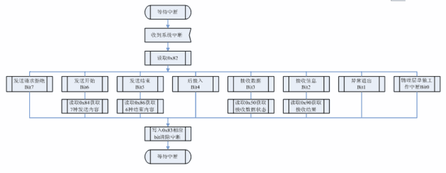
| Interrupts | 0x82 | R | InterRequestDeny InterSendStart InterSendStop InterLateEntry InterRecvData InterRecvMessage InterQuit InterPHYOnly | Bit 7 Bit 6 Bit 5 Bit 4 Bit 3 Bit 2 Bit 1 Bit 0 |
send request rejected transmission is started transmission is complete 'after the access' received data (available?) receiving information 'indicates exit' physical layer receives a single interrupt | |
| 0x83 | W | InterClear | Bits 7..0 | corresponding interrupt register (0x82?) is cleared according to the bit position | ||
| 0x84 | R | SendStartVoice SendStartCSBK1 SendStartCSBK2 Over_VocoderRespon SendStartData SendStartDataPart SendStartDataFull |
Bit 7 Bit 6 Bit 5 Bit 4 Bit 3 Bit 2 Bit 1 Bit 0 |
Voice delivery OACSU request is sent for the first time OACSU requests a second transmission Vocoder config returns an interrupt Data transmission Partial retransmission of data Data are all retransmitted reserved | ||
| 0x85 | W/R | SendStartMask | Bits 7..0 | Enable the SendStart interrupt(s?) | ||
| 0x86 | R | SendStopVoice SendStopVoiceErr SendStopOACSUExp ? SendStopData SendStopDataErr SendStopConfigExp |
Bit 7 Bit 6 Bit 5 Bit 4 Bit 3 Bit 2 Bit 1 Bit 0 |
'The voice ends normally' Exception: End of voice (TX timeout) Voice OACSU waits for a timeout reserved The data ends normally Data abort (transmission timeout) Data acknowledgment timeout reserved | ||
| 0x87 | W/R | SendStopMask | Bits 7..0 | Enable the SendStop interrupt(s?) | ||
| 0x90 | R | RecvDataCRC | Bit 7 | Data fragment CRC test result. 0 = correct, 1 = CRC error. | ||
| .. | .. | .. | .. | .. | The firmware seems to access other regs, but we don't know for what purpose yet... |

| Slot frame type | Coding | "Whether voice" (?) |
| Voice LC Header | 0000 | 0 |
| Voice A | 0001 | 1 |
| Voice B | 0010 | 1 |
| Voice C | 0011 | 1 |
| Voice D | 0100 | 1 |
| Voice E | 0101 | 1 |
| Voice F | 0110 | 1 |
| Voice Terminator | 0010 | 0 |
| CSBK | 0011 | 0 |
| MBC Header | 0100 | 0 |
| MBC Intermediate | 0101 | 0 |
| MBC Last | 0101 | 0 |
| DataHeader | 0110 | 0 |
| DataRate1_2 | 0111 | 0 |
| DataRate3_4 | 1000 | 0 |
| DataRate1 | 1010 | 0 |
| Idle | 1001 | 0 |
| Reserved | 1011 | 0 |
| Reserved | 1100 | 0 |
| Reserved | 1011 | 0 |
| Reserved | 1110 | 0 |
| Reserved | 1111 | 0 |
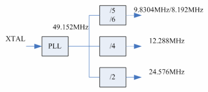
[0x0b] = 0x28 = PLLM ( PLL Multiplier )

[0x0c] = 0x33 = 0b0011 0011
                  |||| \\\\_ PLL input divider,  PLLN  = 3
                  ||\\______ PLL output divider, PLLDO = 3
                  |\________ PLL 'not sleeping'
                  \_________ PLL 'in use' (not bypassed)
XTAL := 29.4912MHz  =: 2.94912e+07
PLLM := 0x28
PLLN := 3
PLLDO:= 3
CLK  := XTAL * PLLM / PLLN / (2*PLLDO)  =: 6.5536e+07
65.536 MHz ? No way. Let's try another formula ("PLLN register value PLUS ONE", based on experience with other chips):
CLK := XTAL * PLLM / (PLLN+1) / (2*PLLDO) =: 4.9152e+07 = 49.152 MHz, q.e.d.
| HR_C5000 | STM32F405 | Note |
| U_SDO | SPI0 data C5000 → STM32 | |
| U_SDI | PE5, "DMR_SDI" | SPI0 data STM32 → C5000 |
| U_CS | PE2, "DMR_CS" | SPI0 chip select STM32 → C5000 |
| U_SCLK | SPI0 clock STM32 → C5000 |

| Cmd | W | IsRead (no default) OPMode | Bit 7 Bits 6..3 Bits 2..0 |
1:next operation is READ, 0:WRITE reserved see list below |
| Cmd | W | IsRead (no default) OPMode | Bit 7 Bits 6..3 Bits 2..0 |
1:next operation is READ, 0:WRITE reserved 011 indicates that the voice code voice data is operated |
| Address | Physical layer mode | Layer 2 mode | Three-tier model |
| 0x00~0x09 | Physical layer data | LC | LC |
| 0x0A | CSBK, Header | LC | |
| 0x0B~0x0C | Custom, Rate1 / 2 | spare | |
| 0x0D~0x0F | Rate3/4 | spare | |
| 0x10~0x12 | Rate3/4 | ||
| 0x13~0x18 | Rate1 | ||
| 0x19~0x1C | |||
| 0x1D~0x23 | |||
| 0x24~0x2F | |||
| 0x030~0x7FF | Text Message |
| Operating(?) | Cmd (1 byte) | Addr (1 byte) | Data0 (1 byte) .... DataN (1 byte) |
| Write control packet | 0x05 | 0x00 | The entire control packet data N <= 19 |
| Read back data pack | 0x85 | 0x00 | Returns the entire packet N <= 9 (?!) |
| Type | Address | Read/Write | Name | ? | Definition | Description |
| Hardware Config | 0x06 | Vocoder638 | Bit 7 | 0: CMX638 interface off, 1: CMX638 interface on | ||
| Vocoder3000 | Bit 6 | 0: AMBE3000 interface off, 1: AMBE3000 interface on | ||||
| DMRFrom | Bit 5 | 0: input from VoCoder,1: input from SPI1 | ||||
| VocoderFrom | Bit 4 | 0: represents output of the protocol layer to the vocoder, 1: represents input of the protocol layer to the vocoder, including self-loopback and custom sounds | ||||
| SPIFrom | Bit 3 | 0 represents protocol layer output, 1 indicates the Vocoder output, protocol layer recording or vocoder recording | ||||
| CodeCMode | Bit 2 | 0 means built-in, 1 means external | ||||
| OpenMusic | Bit 1 | 0 for off, 1 indicates on | ||||
| LocalVocoderControl | Bit 0 | 0 means that the system automatically controls, 1 indicates CPU control | ||||
| Parameter Config | 0x10 | ModulatorMode | Bit 7 | 0 means DMR, 1 indicates FM |
 [0x30]=0x00     [0x31]=0x17     [0x32]=0x02     [0x33]=0xff
 (Mclk/BCLK,hi)  (Mclk/BCLK,lo)  (Mclk/LRCK,hi)  (Mclk/LRLK,lo)