A PCB for Rxcontrol PIC 18F2550 based ADS-B decoder
NEW!
Jetvision.de decided to reissue the PICADSB8 decoder in their shop
Additionally, please check the new development for the FPGA based decoder.
(C) DL4MEA 10/2010
At the moment there are just a few PICADSB9 kits or PCBs left over, and I will not
order new ones but instead concentrate on the next generation. Your
miniADSB receiver will not become obsolete but a very good extension of
that. A web page will be set up as soon as the prototypes are
available. Expected availability in higher numbers is end of this year.

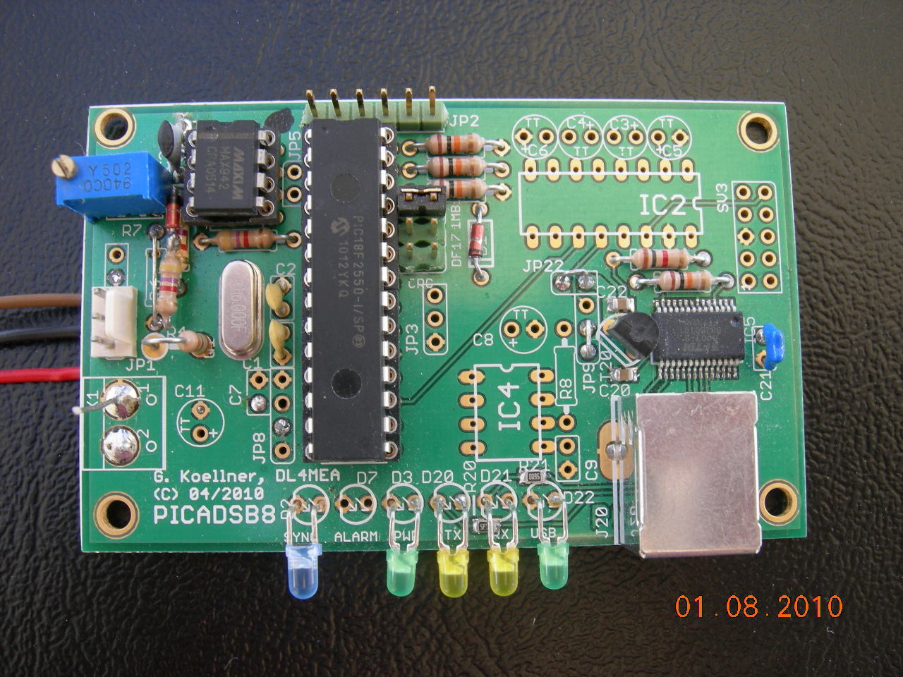
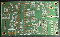
PICADSB
Version 8 (click on it to get a higher resolution top view)
|
Scope:
ADS-B telegrams, as they are
sent from aircrafts on 1090MHz, are widely used as source for a passive
radar system. While in the past the few commercial units that were on
the market appeared quite expensive, Andy presented here
a receiver which has a quite reasonable price and also a very
good performance.
The receiver's output, which actually is a signal level
indication of 10MHz bandwidth around
1090MHz, requires a decoder which transfers the telegrams into
a format that can be
understood by common MMI software, such as COAA
PlanePlotter.
There are mainly two decoders known, an ATMEL
based decoder
solution and the PIC 18F2550 solution by Bertrand Velle, which I choose as
basis simply because I
have a very handsome PICKit-2 programmer. I also added an RS232 to USB
converter in order to interface easier to all PCs, to connect several
units to one PC, to provide power and, as it developped over time, also
to increase the data rate by a significant factor. |
Let me say a few words about the meanwhile 3 versions that I provide:
This development would not have been possible without the
response of the users. All experience that is brought into this circuit
was only possible because it is widely used and the bottlenecks were
discovered by using it under various conditions. The recent PICADSB9
meanwhile shows to be the very best of all, doing its job pretty
perfect and satisfying all requirements. Since the improvements were
mostly done at the AD converter, I provide all information how to
modify the elder boards in case that you have problems with nearby
planes (doughnut effect) below.
As soon as a lately discovered bug in Planeplotter's local
decoding is removed, I can show the range that I can receive with my
simple setup.
For the future we are planning a few more improvements, but these will
require some more time to develop, also much time has been spent for
this project and other things had been dropped, so it will be a little
bit slower.
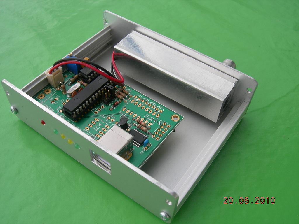
The ready unit
With a slightly modified miniADSB (connector leaving at the bottom) and PICADSB8/9, these 8 units were built.
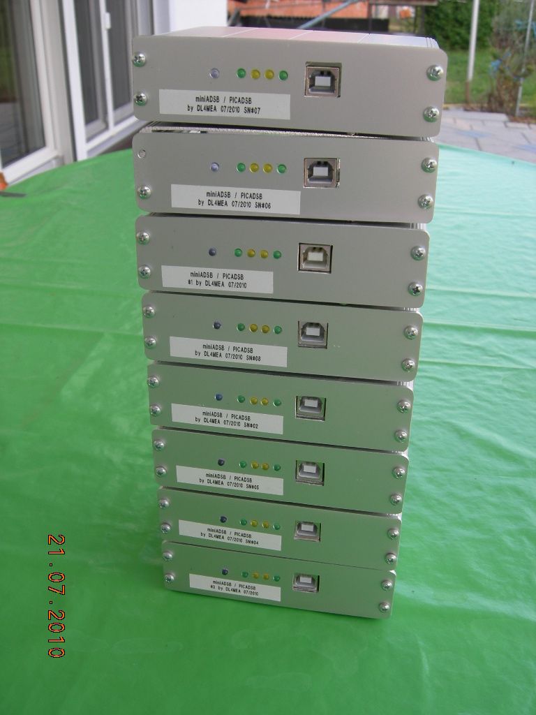
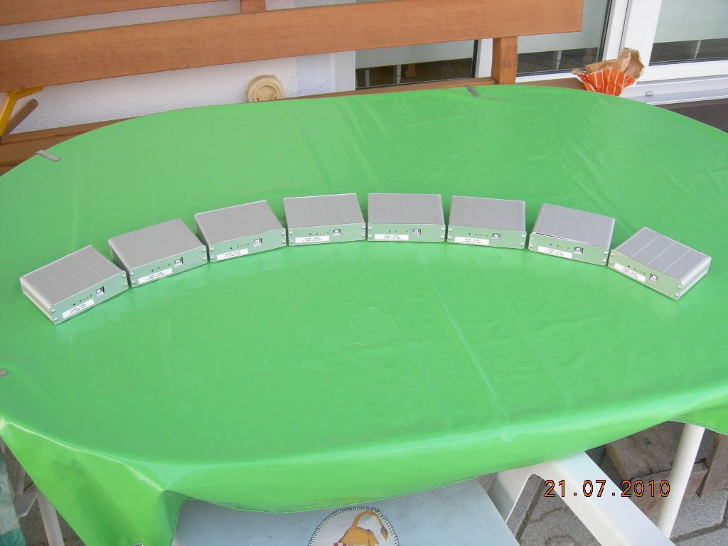
All are already spoken for some friends, but for futher
questions how to get one of these units, please scroll down to the
chapter "future".
Links:
ADS-B Telegram Format
MiniADSB Receiver and Forum
RxControl
web page by Bertrand Velle, and blog
in french (translated
to english by google)
COAA
PlanePlotter GUI software
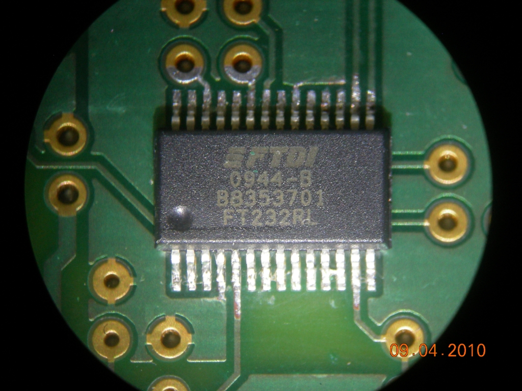
FT232RL Serial to USB converter and driver
Antenna
that I am using but with only quarter wavelength radials (see also FAQ
section)
A possible transmitter,
intended for use on ultralight planes.
Schematic:
(click on the image to get PDF)
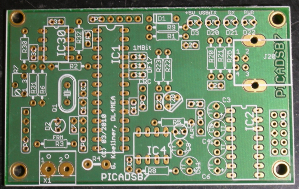
Here you can get the PICADSB8 schematic (PDF)
Here you can get the PICADSB7 schematic (PDF)
Description:
Basically this is the decoder circuit as
introduced by Bertrand Velle with some extensions.
Serial Interface:
There are two options for the serial interface: Standard
RS232 using a
MAX232 or Serial-over-USB using an industry standard FTDI FT232R
converter. The driver for this can be found here.
You can output data
on both ports at the same time, but only receive control commands from
one interface, which has to be selected by Jumper 9:
| Jumper JP9 |
1-2 |
2-3 |
| Serial Control |
Standard RS232 (MAX232) |
Serial over USB |
Powering from USB
After the port enumeration, the
power for the PIC and the receiver can
be supplied from USB. There are so many decoupling capacitors on the
board and I did not see any performance degradation compared to
supplying the receiver from an external, high quality power supply.
| Jumper JP22 |
1-2 |
removed |
| Power
from USB |
powered
from USB |
external 5V supply (using
connector X1) |
In the current design, and as the kits with pre-soldered FT232
are
delivered, the power to the PIC is always on. In case that you do not
like this but have the power applied just after enumeration, download
the tool from FTDI's web page and reconfigure your FT232 to get
permission for 250mA right and switch on power after getting permission
from the PC.
Input connector JP1
To make clear how the input connector JP1 is wired.
| JP1 Pin |
Function |
miniADSB suggested color |
| 1 |
+5V
(use 47R as Rfuse) |
red |
| 2 |
GND |
black |
| 3 |
analog
input |
blue |
| 4 |
GND |
leave free |
| 5 |
RSSI
input |
leave free |
Analog to digital converter
PICADSB7/PICADSB8: The board also includes a
comparator circuit around IC30. The reference
is built through a low pass filter 470k/56pF. With this, the comparator
level is aligned upwards when strong signals are received.
The input signal must be shifted below the comparator level, which is
done using the poti R7 and resistor R6. Adjust this for highest
sensitivty, means a maximum telegram rate at all.
PICADSB9: With the
experience of the two versions we found that the comparator's reference
doesn't raise quickly enough at strong signals. The combination of
D31/R33 now does this much quicker, and so does R31 discharge with
around 10 times longer time constant. Additionally the biasing is done
in a different way now, removing the DC part from the input signal with
C12 and re-biasing below the comparator's reference level through an
adjustable DC voltage. This will keep the amplitude of weak signals
unchanged!
This is also close to the improvement suggestion for ADS-B reception
which is telling to set the comparator level to the top signal level
minus 6dB. More about this further down on this webpage.
I regularily see planes in a distance of 220nm with this decoder, and
do not have a doughnut effect for the planes passing by for the local
Munich airport (and if I say close, they are at around 2nm
distance).
There is an option to supply an
already digital signal to the input. Since this is a very basic system
design decision, it is done using a solder bridge on the solder side.
In this case that you select this option, ommit at least the poti R7
and R31.
| Solder
bridge SJ1/SJ2 |
SJ1 |
SJ2 |
| Analog
to digital conversion |
analog
input
local AD converter
(as for miniADSB receiver) |
digital
input
external AD converter |
Place
plan and bill of materials: (click
on the
image to get PDF)
The new PICADSB8 board has some minor cosmetic changes:
- The LEDs and the USB connector are aligned on the long side
of the board, so it can easier be mounted into a box
- There is a Push-Pull comparator used, which will provide a
better signal to the PIC (this is part of the semi-kit)
- The LED current limiting resistors 680R are SMD and the
100nF blocking capacitors (also part of the semi-kit)
- The two additional resistors that avoid the oscillator
problem are part of the PCB
- Instead of the LM311 a new Push-Pull MAX942 is used (later removed, did not improve reception)
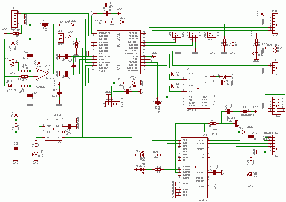
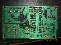
PICADSB8 top components
 |
PICADSB8 bottom components
 |
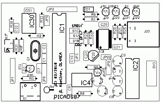
The new PICADSB9 board has a major functional improvement in the AD converter (see in detail below):
- Returned to the LM311 comparator, which is much cheaper. The pullup was made 820R for a faster raising edge
- Cosmetic change: Leaving a little bit more space for the potentiometer R7
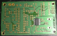
PICADSB9 top components
 |
PICADSB9 bottom components
 |
Basic
parts - always needed
R1
R2 10k
R3 R9
680R
(2)(4)
R4
FUSE or 33R
C1
C2 22p
C10
100n (4)
C11
47µF (5)
C7
47n (5)
D1
1N4148
D2
LED 3mm blue
D3
LED 3mm green
IC1
PIC
18F2550
Q1
Crystal 16MHz
JP1
5 or 3 pin header
JP2
6 pin header (1)
JP5
2 pin
header (1)
JP8
4 pin header (1)
JP9 JP3 3 pin header
S1A S1B S1C
2 pin header
(1) may be ommited if not used
(2) see extra note about resistors used at LEDs below
(4) SMD 0805 for PICADSB8/9
(5) Some users reported problems if this capacitor is equipped
Important Note:
On PICADSB7, you have to solder two
resistors 10kOhm to the bottom of the PCB! (see below)
|
Parts that are needed if using
RxControl alarm function
R5 560R (2)(4)
C9
47n
C8
2µ2
D3
LED 3mm red
IC4 NE555
Parts that are
needed for USB interface
R20 R21 R25
680R
(2)(4)
R22
10k
(3)
R23
1k
(3)
C20 C22
100n (4)
C21
10n
D20 D21
LED 3mm yellow
D22
LED 3mm green
IC5
FT232RL
T20
BC558 (3)
J20
USB female Type B
JP22
2 pin header
or bridge (3)
Parts that are needed for
standard RS232 interface
C3 C4 C5
C6 10µ
IC2
MAX232
SV3
10pin 2row pin header
(3) only used if power over USB is used |
Parts that are
needed if using the LM311/MAX942 analog to digital converter
PICADSB7/8 components:
R6
4k7
R31 470k
R32 820R
R7 4k7
spindle trimmer
C31 100n (4)
C32 56p
IC30 LM311N
IC3 MAX942
PICADSB9 components:
R6
4k7
R7 4k7
spindle trimmer
R31 47k
R32 820R
R33 4k7
R34 470k
C12 100n (4)
C31 100n (4)
C32 82p
D31 1N4148
IC30 LM311N
Hint:
From PICADSB8 on, I also provide a 3 pin cable free of
extra charges. Swap the black and the brown cable before
mounting! The spring in the connector can be released with a
sharp knive easily. Then the colors are:
Red = +5V
Black = GND
Brown = Signal
|
Change History:
26.03.2010:
R32 is 1k instead of 1k8
30.03.2010: Not for PICADSB7, but the
miniADSB
receiver: Add a 10kOhm SMD across the input if you are using an antenna
which is not grounded
10.04.2010: R30 is 0R instead of 10k, R7
is 4k7 spindle trimmer
11.04.2010: R3 R9 R20 R21 R25: Adjust to
your LED current: (5V - ULED) / ILED,
suggested 560R is for low current LEDs
13.04.2010: add two 10k to bottom as
described below (these are to solve the oscillator on/off problem)
02.05.2010: rewrote R2 (10k) to the parts list.
05.05.2010: added PICADSB8 information
25.05.2010: if you have problems with your PIC operating
correctly, first remove C7. If still exists, then also remove C11
28.05.2010: on PICADSB8 the comparator is a MAX942
29.05.2010: Improvements added (see below), hint added how
to use the cable that comes with PICADSB8 (see parts list)
17.06.2010: PICADSB9 introduced
01.08.2010: R4 changed to 33R, top photo (1st in web page)
replaced, note about power control settings added in RS232 setup section
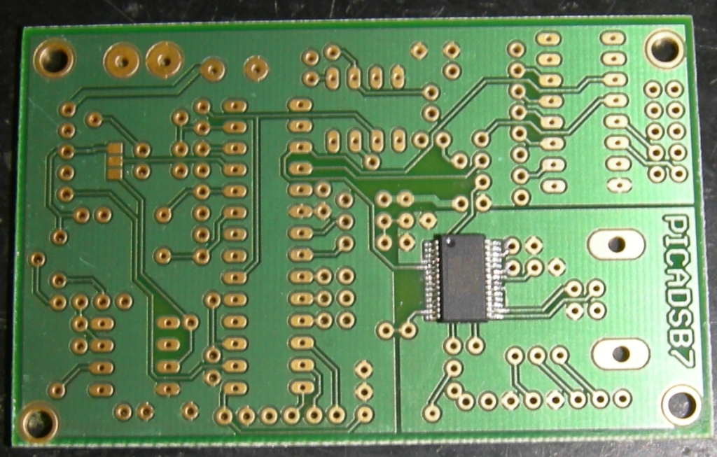
Some pictures of the PICADSB7 PCB
PICADSB7 PCB top |
PICADSB7 PCB bottom with FT232 |

FT232 soldered to bottom |
Important
Note: On
PICADSB7, you have to solder two resistors 10kOhm to the bottom of the
PCB. With some PIC types, the oscillator switches on and off in an 5sec
time frame without these:
 see at top, middle
(click on the picture for larger version)
see at top, middle
(click on the picture for larger version)
RS232
Set Up:
If you are using the standard serial interface with MAX232,
setting
up the connection to the PC is pretty common and shall not cause any
problems.
In case that you decided to use the Serial over USB, the
operating
system will probably ask you to install an USB driver when connecting
the unit for the first time. You will find the on FTDI's web
page here.
After you have installed the driver, open the device manager and check
which COM port became assigned to the new unit. That is the number you
have to use in your MMI application.
There are 6 LEDs on the board:
| LED name |
suggested
color |
meaning |
| D22 |
green |
USB is plugged |
| D21 |
yellow |
blinks when data are
transmitted from PICADSB to PC via USB |
| D20 |
yellow |
blinks when PICADSB
receives data from PC |
| D3 |
green |
ON when PC has enumerated
(recognized) the USB port |
| D7 |
red |
alarm LED |
| D2 |
blue |
SYNC LED: flashes whenever
a telegram start was received and is beeing processed |
There is a transistor on the PCB that allows power switching.
Unfortunately the default setting of the FT232 initialisation of the
newer devices is different, or my 1st samples were not standard, due to
that I connected the power switching device to a wrong pin. If you see
both green LEDs on immediately after plugging the USB connector, then
you have this issue.
If your unit works, don't need to change.
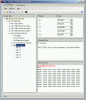
If you see reset problems, download the FT_Prog tool from FTDI's web page, and change the setting of IO Controls C2 to PWRON# as shown in this picture.
Afterwards, you will see the LED besides the USB connector going on
immediately after plugging in USB, and the other green power LED just
lightens just after the port was detected by the PC (bell in the
loudspeaker)
Initialisation:
In case that you connect the unit for the first time, for
testing
purposes, open a simple terminal application to the COM port
that PICADSB uses. (Most users have Hyperterm (which cannot handle 1MBit) available, but
there
are also Teraterm or Putty).
Jumper S1C selects the serial interface
parameters:
| Jumper
S1C |
removed |
1-2 |
| Serial
Interface |
115kBit,
8Bits 1 Stopbit, no parity, no handshake |
1MBit, 8Bits 1 Stopbit, no
parity, no handshake |
The RxControl software supports several data formats. The AVR raw format (Type
"3") is are just a hexdump
of the received frame. With this format the decimal conversion of the
received data is done in the MMI software, for example PlanePlotter. On the terminal, it looks like
*8D484395990052B2E80B027D687F;
*8D3C65039990FB9E286404A0043E;
*8D4BAA499945161668800268C26E;
*8D3C662B903D006914A84A707D6A;
*A028023C2010C231595820AA9001;
In case that you want to see the messages in the RxControl clear text
decoded format (Type "1"), you have to enter your
own coordinats in HEX format to the PIC. Here is how you convert your
location into hex:
| Format |
Longitude |
Latitude |
| DD MM SS |
48° 21' 56" |
11°
28' 42" |
| divide
seconds by 0.06 |
56 / 0.06 = 933 |
42 / 0.06 = 700 |
| DD
MM.MMM |
48° 21.933' |
E 011° 28.700' |
| remove
comma |
004821933 |
001128700 |
| convert
to hex |
0x004993AD |
0x001138FC |
Now, in the terminal application, press 'P' button (capital
letter!) and enter
the LON and LAT values from these hex values.
Then you will get an output like this:
+,0,17,3C1193,,,1,49.222290,11.221088,20700,,,,,,;
+,0,17,4BAA4B,,,1,47.995777,12.357646,34975,,,,,,;
+,0,17,40600E,,,,,,,,-64,333,-249,,;
+,0,17,3C4984,,,1,48.425453,11.477677,8850,,,,,,;
+,12,17,40600E,,,1,48.533550,11.472689,35025,,,,,,;
+,0,20,300096,,,,,,4525,,,,,,;
+,15,17,40600E,,,,,,,,-64,333,-249,,;
+,10,17,4BAA49,,,,,,,,0,-278,183,,;
FAQ:
What is so
special with your AD converter?
The AD converter is using a very short time constant in order to create
the comparator's reference and herewith somewhat aligns to the signal
strength, strong signals will be decoded as well as weak signals. I
live in the approach path to Munich airport's runway 28L and some
planes are even flying over my house. These are decoded as well as
planes up to a distance of 200nm. There is no doughnut effect.
How can I
distribute processing load in the best way?
The RxControl software does not receive and decode in parallel due to
processing power. Let Planeplotter do the decimal conversion, use the
AVR raw format (format '3').
I will get the PIC in the
kit preprogrammed. How do I update it later?
There are many PIC programmers described in the internet, which allow
programming of the PIC. I cannot suggest a special one. If you point me
to some descriptions, I can have a look at them and later name them
here.
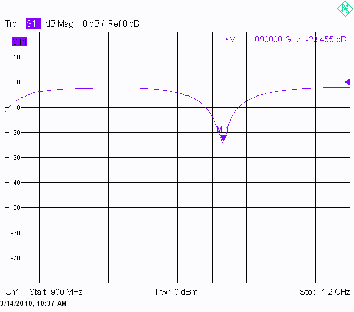
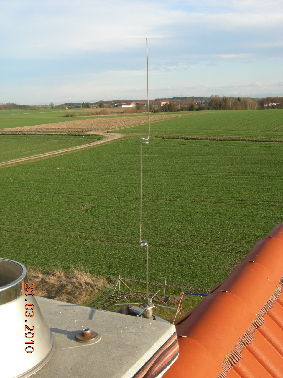
What is the best antenna?
I am using this antenna but with
quarter wavelength radials only. Don't know what the author hopes to
gain from longer ones. I have measured one on a network
analyzer. If you leave the antenna rod in free space (as in
the
picture below), make the top section about 2mm longer, if you put a
20mm plastic tube over it, shorten the top section by 5mm. I do not
know the influence of a wide diameter (50mm - 100mm) plastic tube,
maybe this is then just matching the given length.


Click on the pictures for higher resolution (drawing from orignal web
page, in order to copy before it disappears there)
A final note for manufacturing: Take a long wire and put markers for
the
sections on it: 136mm -> 65.5mm -> 205mm -> 65.5mm
-> 190mm.
Then first
roll the inductors (1.5 turns onto a 9.5mm drill) and second do the
90° bends in order to get it straight.
Note: Add a
10kOhm SMD across the input if you are using such an antenna which is
not
grounded in order to prevent ESD descruction of the SAW and the first
amplifier!
Another good antenna, which is easy to build (you may leave away the loop with acceptable degradation) can be found on Edward's page.
Which connectors and
which cable shall I take for the antenna?
I suggest using an N connector for it. Do not use silicone for
waterproofing, since this never makes it waterproof. There is Spinner
PLAST2000, a special more fluid silicone, quite often offered for a
reasonable price in eBay. Once you have seen this working, you will
never use silicone again.
Which cable shall I use
and does a preamplifier improve my reception?
Up to 5m a RG58 is sufficient, up to 15m you can use RG213, and above
that you are starting to get losses. I am currently using 25m long
HCF1/2" cable, which is high quality cable with just 3dB insertion
loss. For longer cables, you may try to use a simple preamplifier which
was built for 23cm amateur radio band in order to improve the
reception, but don't
use one with 2 stages and don't use such which
have filter for 1296MHz built in.
You only have to overcome the cable loss, otherwise you may get
problems with strong signals. (These are assumptions from my experience
as a radio amateur and not based on measurements!)
Which range can I expect seeing planes?
Of course this mainly depends on the location of your antenna. Some
nearby or flying over planes can be received indoor and with just a
screwdriver in the antenna connector once the poti is aligned correctly. We did so quite often just for fun.
Otherwise, we've seen planes up to 225nm distance regularily. With
PICADSB7/8 and when aligning the poti there for highest sensitivity, it
got the doughnut effect. PICADSB9 no longer has this effect, I see the
nearby Munich airport (15nm) as well as 225nm distant planes. I do not
have a preamp! Just by this I now discovered that the local decoding in
Planeplotter is not sufficient because it puts all planes into my own
CPR segement, instead of the 5 ones that I really receive the planes.
This performance, in my opinion, is incredible!
AD Converter Improvement:
After using the miniADSB receiver together with the PICADSB decoder for
a while, we got some experience about the problems of the decoding
of the input signal into a processor's digital signal.
These problems are known to those who life close to an airport or have
a lot of very near flying aircrafts. If you do see planes up to 150nm
or even more and if you do not suffer from seeing a gap at nearby
planes, please don't read further. Keep it as is and be satisfied. You've been warned.
In my case, living at the landing path of one of the Munich's airport
runways, I often missed planes passing by at a distance of 800ft or so
when the poti was aligned for highest sensitivity and most distant
planes. We (it means Andy and I) investigated the reason that the
AD8313 detector has a very slow and delayed falling edge when it
receives strong signals. If then the
comparator is working with a very low reference voltage, the PIC cannot
see the '0' in the 2nd phase of the bit. Chances to make the RF decoder
faster are expensive and we do not want to touch the RF part since it
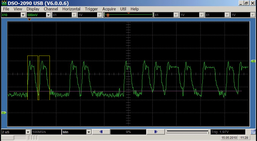
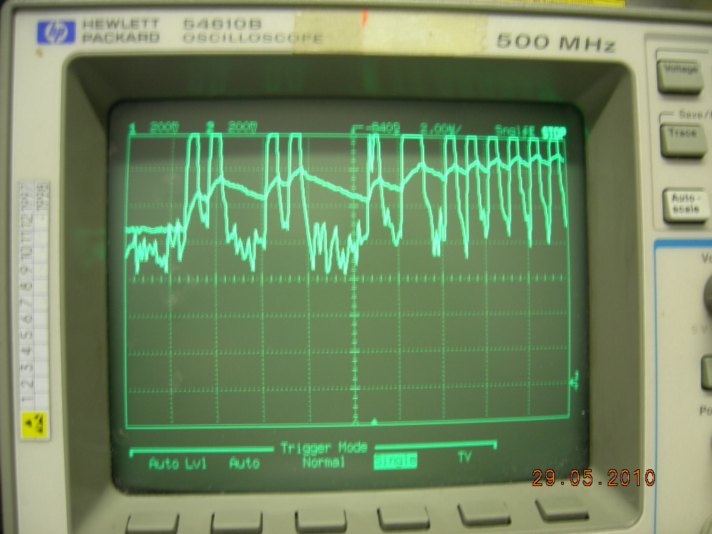
is complicated but stable. This picture shows an extreme situation:
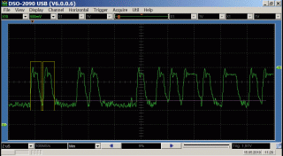 |
Green: ADS-B signal
Magenta: Comparator reference
Yellow: Output of AD converter
It is clearly visible that the PIC, which samples the input at 25% and
75%, reads a '1' at both times and so does not recognize the sync at
all. |
So it is necessary to raise the comparator reference as quick as
possible and then hold it for as long as the frame lasts. First idea
was to use a Sample & Hold circuit controlled by the PIC, but I
found it much easier. Here is the modified circuit:

|
As you see, the RC combination was
made a little
bit faster, using R31 (47k) and C32 (82p). But it will even be
charged faster using the diode D31 and R33 (4k7). Due to the
voltage drop across the diode the reference always stays around 200mV
below the voltage peaks.
The result can be seen on the right side. The reference level (in the
middle) raises quickly and drops slowly. Even in the middle of the
signal, it is defined fine in the upper half of the signal; a methode
which is also suggested in some official documents.
This modification can be done very easily by exchanging components on the PCB and soldering D31 and R33 across R31.
NOTE: The modifications are shown for an LM311 comparator. Pins at the MAX942 in PICADSB8 are different! |
 |
There is another modification visible in the above excerpt
from the schematic: The input signal is no longer totally
attenuated to go below the comparator's reference. Instead, the AC part
is split away from the input and a DC bias is added through a high
value resistor. Due to this, especially low amplitude, weak signals,
are kept with their worthful original amplitude.
- For this modification I suggest to bridge R6 in PICADSB7 and PICADSB8.
- Also, you have to cut two traces: The one that goes from the
signal input (JP1, Pin1) to the poti (solder side), and the wire from
the poti's slider to the comparator (PICADSB7: solder side, PICADSB8:
top side, below the poti).
- Use a 100nF (prefered axial -like resistors-) capacitor and connect the input to the comparator input
- Use a 470k resistor and connect the potentiometer's middle pin to the comparator input.
- Use a 4k7 resistor and connect the potentiometer's pin that was
connected to the signal input before to any pin that carries +5V (or
use a leakage at the bottom copper plane)
- As a check: with a DC voltmeter you now must be able to set the DC voltage at the comparator's input from 0V to 2.5V.
WARNING! Last modification is a little bit
complicated and you know what you are doing. There is no warranty
neither a repair service for damaged boards.
 |
This shows how I modified the PICADSB9 PCB in a semi-perfect way:
R31 is replaced by a standard 47k resistor, the 1N4148 diode is
soldered just over it, between the cathode of the diode and R31 there
is a small SMD 0805 4k7 recovered from miniADSB because I only install
the one between Pin 7 and Pin 8 and ommit the pullup and protection
resistor there.
Besides the SMD resistors, you can also see the PCB trace cut off that leads from the poti's wiper to Pin3 of the comparator. |
![[HOME]](../icons/home.gif) Last updated 04.10.2010 07:00 ((X) home () Munich, St. Martin Straße, S-Bahn station) by
DL4MEA
Last updated 04.10.2010 07:00 ((X) home () Munich, St. Martin Straße, S-Bahn station) by
DL4MEA