Old 23cm Modulator

Old 23cm Modulator
Features:
1) All components should be easy to find (in Auckland).
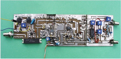
23cm Circuit Description:-
The incoming video signal goes via a PAL pre-emphasis network which is DC. coupled to pin 1 of I.C.1 (NE592 modulator). Pin 1 is biased to approximately half supply rail voltage mainly by means of the two 1.5k resistors connected to it. The sound IF, typically a 5.5 MHz carrier or with an additional second carrier of 5.74 MHz is AC. coupled in, after the pre-emphasis network to pin 1 of IC. 1. The second input, pin 14 is also biased at about 1/2 supply rail. VR 1 alters the amount of signal gain / deviation of the FM signal by changing the amount of internal feedback inside the NE592. VR 2 allows a small amount of H.F. boost which can be omitted, if not needed. Pins 7 and 8 of the NE592 are the positive and negative going outputs, one of which is connected to the top end of VR 3 bias trimpot.
VR. 3 sets the bias via an air wound choke to varicap 1 to give best modulation linearity. The wiper is typically 4.5 Volts plus or minus 1/2 a Volt. Adjustment of this also alters the overall FM deviation, so re-adjustment of VR1 may be required.
The oscillator consisting of TR1 (BFR91) in common base arrangement, a microstrip, two varicaps and several other components, is based on an early B.A.T.C. design which has been modified for this particular application. The base is coupled to ground via a SMD capacitor, with positive feedback being provided by the 68 ohm emitter resistor and inductance from the 1.5 turns (3mm diameter) choke wound using the resistor's pigtail lead. The frequency is set by the combination of the 2 varicaps, the length of the microstrip and to a lesser degree, other reactive elements of the oscillator.
Two varicaps are used so that the deviation is reasonably constant throughout the VCO tuning range. This is done by keeping the average bias voltage constant on varicap 1, and varicap 2 has the dc. tuning voltage applied via an air wound choke to adjust the FM carrier's centre frequency. The oscillator can be used without the P.L.L. circuit by adding VR 4 to varicap 2 to give the desired tuning volts. Connection between the 2 varicaps is made by a 4.7 pf or two paralleled 2.2 pf SMD capacitors. If the V.C.O. is working as intended, there should be around 0.5 of a Volt for 1200MHz output, and around 11 Volts for 1300 MHz. Moving the connection point of varicap 1's anode up or down the end of the microstrip by a few millimetres will alter the frequency range if the full range can not be had to begin with.
The second microstrip samples a small amount of the oscillator signal and via Cx1, couples it into the base of TR2 (BFR91). Cx1 is about one "twist" of insulated hook-up wire about 5mm in length giving around 1/2 pf worth of capacitance. If Cx1 is too great and results in over-coupling, then TR2 can sometimes break into spurious oscillation at around 1.8 GHz. Some typical symptoms are that any attached PLL will not lock and the DC tuning voltage does not have any effect on the output frequency. TR2 is a common-emitter amplifier stage which feeds the IC2 pre-scaler and the IC3 pre-driver stage. Cx2 connects to the input of the IC2 (SAB6456). It is made up of insulated hook-up wire about 7mm long that sits along the collector lead of TR2.
IC 2 (SAB6456) is a divide-by-256 pre-scalar IC that has it's output connected to the PLL board. The legs of the IC are cut short so that the body may sit flush with the PCB for best operation at 23cm. The output should read between 4.8MHz and 5.08MHz which is suitable for coupling into the hi-Z PLL input.
An 8dB pi-pad, which helps to give some degree of isolation, is connected between TR2 and the input of the IC3 (ERA-5) pre-driver MMIC amplifier. A de-coupled 9.8 Volt supply is fed to the output pin via a resistor and 3-turn air-wound choke to supply power to the ERA-5. The output signal is coupled via a SMD capacitor to the next stage.
IC 4 (78L08) provides a nominal 9.8 Volts, increased from it's normal 8 Volts, by means of an amber LED in series with it's ground pin (white, red, green or blue LEDs are not suitable as their voltage drop is different). A 5 Volt supply to the pre-scaler IC and for TR2 base biasing is provided by a standard series resistor-Zener combination and smoothed by a 1nf SMD bypass capacitor.
Other additions that can be used for SHF ATV : Frequency read out display, Video processor, Dual Sound Carrier, 15 watt power amplifier. Teletext boards for test cards, FM ATV Receiver, 23cm Line Amp and 23cm Ga-As FET preamps.
Text / Drawings Copyright (C) 2001 ZL1WTT / ZL1VFO

M67715 Amplifier by ZL1WTT
The exciter stage feeds RF through the bandpass filter to the pin 1 input of the M67715 Hybrid Amplifier module. Pins 2 and 4 are the + 8 Volt supply pins, with pin 3 as the gain control pin and pin 5 the final output.
The LM2941 regulator does 2 different jobs.
1) The PLL lock detect line is connected to the on/off control pin. When the PLL controlled oscillator drops out of lock, the bias voltage will drop and the Tx amplifier will be shut down.
2) The gain of the M67715 is controlled by the bias voltage from the regulator. This is normally set at around about 4 to 6 Volts and is adjusted by the 25k trimpot. The 7808 regulator feeds to the M67715 as well as the LM2941 regulator.


PLL Section
The Phase Lock Loop circuit is made up of 3 ICs from the 4000 CMOS series, consisting of a 4060, 4046, and 4059 and TR1, TR2 .IC1 is a 4060 which has a crystal reference oscillator formed around pins 10 and 11. The 4MHz reference is divided by 1024 producing a 3.90625kHz signal available at pin 15. This divided reference signal is supplied to IC2. IC2 is a 4046 which is used for it's Phase comparator section. IC2 feeds out the dc control voltage via a R-C integrator from pin 13. The lock detect signal comes from pin 1 through a second delay circuit to transistor TR2 (2N2222A). It works as a three-second delay switch for the LM2941 regulator on 2 watt amplifier board.
IC3 is a 4059 programmable divider. A small sample of the 23cmoscillator signal is divided by 256 by the on board pre-scaler chip, and isfed to the base of the TR1(BC549) transistor. It outputs a 12 Volt logic level to the input pin of IC3. The 4059 ICs are set to the divide by 10 mode, which allows programming in standard BCD mode. It divides the input frequencyby the divisor set by the programming pins and outputs a 3.90625kHz square wave as a result (When in lock) to the 4046 for comparison against the divided down crystal reference Signal. By changing the logic states applied to the programming pins of the 4059, the TX frequency can be set to any frequency in the 1200-1299 range in 1 MHz steps.
Some example 23cm frequencies --
1250 MHz 0001,0010,0101,0000
1281 MHz 0001,0010,1000,0001
(C) 2001 ZL1WTT ZL1VFO