A SIMPLE GPS DISCIPLINED REFERENCE
By Murray Greenman ZL1BPU
A straight-forward GPS reference, with real time clock.
Use GPS 1pps reference and a high performance OCXO.
INTRODUCTION
This design came about as a result of efforts to design a high stability reference
which locked to a 10MHz source. With some minor hardware adaptation and completely new firmware, it proved
possible to design an excellent GPS Disciplined Oscillator (GPSDO) using the same circuit board.
The design gently locks a high performance 10MHz OCXO to the GPS or other 1pps reference, and
is capable of providing an accurate reference, with high stability at the
level of a few parts in 1012. The unit operates without requiring any intervention or control.
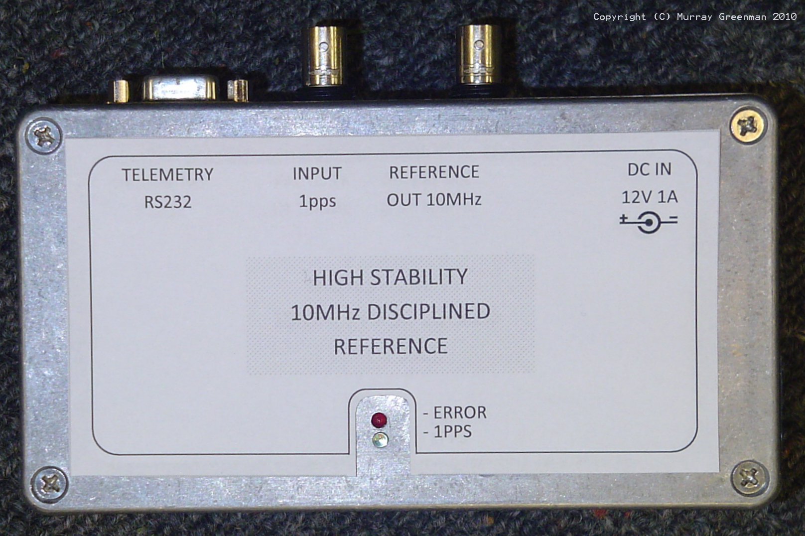
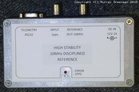
A serial link provides telemetry and a user-set real-time clock. Controls are provided for
initial calibration. The OCXO sine wave output can drive 50 Ohm loads (1V p-p).
There is also an optional regenerated CMOS 1pps output which can be used to
operate other devices, and it would be easy to swap this for a CMOS 10MHz output instead.
The Simple Reference in Hammond box
Dimensions: w=150mm h=100mm (including connectors) d=55mm
(Click on image for a larger view)
The clock and reference continue to operate when GPS is lost, and although the
reference frequency will then very slowly change due to OCXO ageing,
it is held digitally at the current operating point until GPS returns. The clock
will be accurate to parts of a second per year (provided power is not lost),
even if GPS is occasionally or frequently lost.
Here is a summary of the special features of the Simple Reference:
- 10MHz GPS disciplined reference accurate to about 0.5mHz (5 x 10-11)
- Stability (Allan Deviation) much better than 1 x 10-11 (depends on OCXO)
- Completely reliable real-time clock, set to UTC or local time
- Ride-through (holdover) operation with GPS lost <1 x 10⁻⁹/day (depends on OCXO)
- Serial control and telemetry - long term phase, frequency and stability plot on PC
- High performance 16-bit maths, 14-bit PWM monotonic frequency control
- Uses high performance OCXO with built-in voltage reference
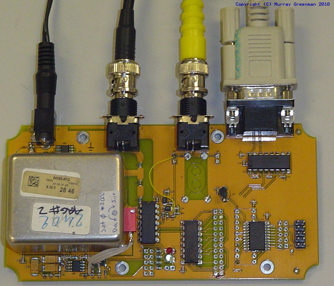
The Simple Reference can be built on a two-layer PCB
The unit is not difficult to build, although performance will be best if a double-sided PCB
with extensive ground plane is used.
There are six ICs and one transistor. One of the ICs in the photo above is not used. The prototype
used surface mount components extensively, mostly to save space. There are no components on the back
of the board except the LEDs, which are fitted when the unit is placed in the box.
The circuit board shown above was designed to fit into the lid of a standard Hammond 1590WP1 diecast box on 10mm spacers.
No, I cannot supply
circuit boards, boxes or other parts!
The high stability performance is achieved through the use of a
high quality SC-cut Oven Controlled Crystal Oscillator (OCXO). This is the most expensive component in the unit,
and must be of the 12V operated type with an ~8V reference output, since this temperature controlled
low noise reference is used to operate the voltage control circuitry. The
RAKON CFPODO family is ideal.
Other manufacturers (Vectron, TEMEX, Morion, Trimble, NDK etc) make similar products. Suitable devices
can often be found on internet auction sites for US$30 or so. Use the best oscillator you can afford.
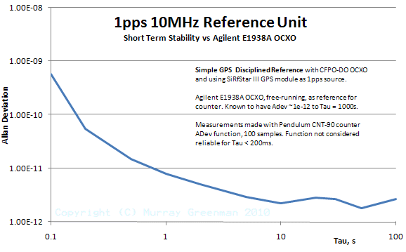
Short Term Stability Performance of prototype unit using CFPO-DO3 OCXO
The serial
data can be used for time and performance logging, or could be adapted as an SNTP source. The real time clock is independent of GPS time, but has the same accuracy as the reference. The clock can be synchronized to within a few ms of the 1pps reference. The phase and frequency information
can be used for calibration or long-term tracking of the reference oscillator performance.
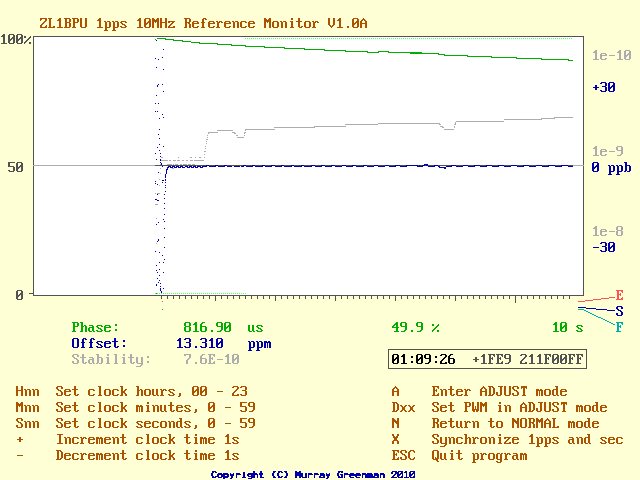
A special companion PC monitoring program 1PPS10A has been designed for this unit,
and is supplied with the firmware.
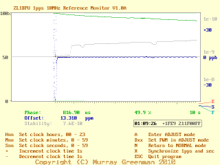
Oscillator performance monitoring with 1PPS10A
(Click on image to view full size)
The main chart (see above picture) scrolls from right to left with time, and has a time scale of minutes, 10 minutes and hours below.
Three telemetry values are plotted on the main chart:
- The PWM duty cycle % is plotted in green (resolution 0.006% dark green, resolution 0.1% dotted light green)
- The offset frequency calculated by the unit is displayed in dark blue (8x LSBs), range �30ppb
- The stability estimate, based on how many seconds have elapsed since a phase change of 100ns
was detected, is displayed in grey. This is a log value, range about 4 x 10⁻⁷ to 1 x 10⁻¹⁰.
The default chart speed is 10s per step (1.5 hours across). The chart speed can be changed via a run-time
script parameter, and is easily set for 24 hours or more to be seen at a glance. The chart sampling rate
is constant at one sample per second, so no data is lost at lower chart speeds. No data is stored, however, so if you
want to analyse the data in different ways, you will need to write your own program or spreadsheet script to capture the data.
Beneath the graph, three status flags are plotted, so it is easy to tell if a change of state has occurred.
These flags (ERROR, SETUP and FAST) are shown as colour coded dots or lines.
Various telemetry values (reference phase, frequency offset and stability) are also reported as text,
again colour coded to match the graphs. Within the black box at the right the complete telemetry string is displayed, showing the
time and other values. The information is transmitted every second just after the regenerated 1pps event,
and will be received completely before the 50ms duration 1pps output pulse ends.
The picture above illustrates the first hour or so after a warm start. You can see the PWM value slowly dropping as the oscillator stabilizes. At the same time, the stability steadily increases. Steady state is reached after about 10 hours, although the OCXO is
within �2ppb (2 in 10-9) within two minutes (10 minutes from cold).
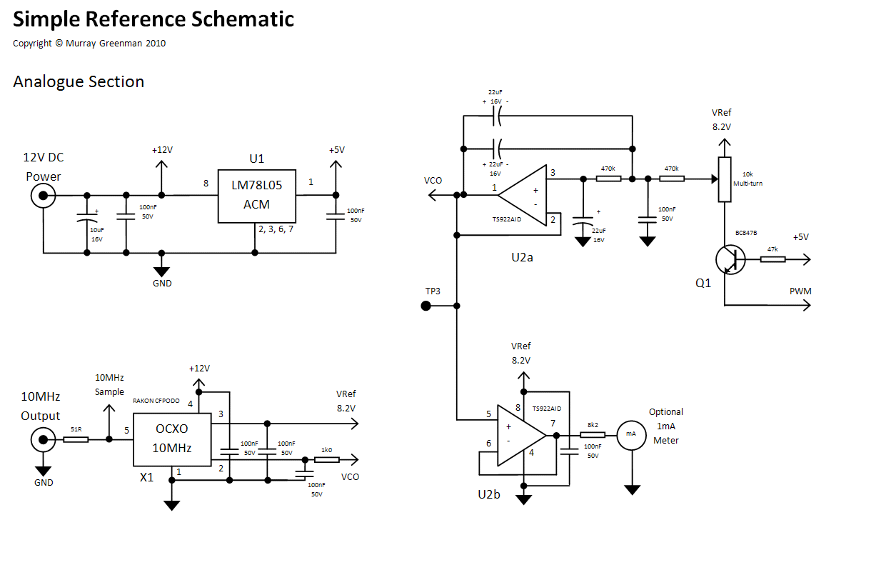
DESCRIPTION - ANALOG SECTION
Follow the full-size Simple Reference Analog Schematic as you read this description.
Power for the unit comes from an external 12V regulated source (typically a switch-mode wall-wart), which
directly operates the OCXO. The connector is the usual coaxial power connector. A small regulator U1 provides power for the logic section. No standby power is provided, although a 12V 7AH SLA could be used with an appropriate switch-over diode and charging arrangement. The steady state current draw from 12V is 200mA,
and the same supply could operate the GPS module.
The OCXO X1 has an internal buffer designed to drive 50 Ohm. The output is able to drive 1V p-p into
50 Ohm (+4dBm). The series resistor can be omitted (gives +10dBm) if there is no risk of
mis-connection which may cause damage. The OCXO
provides a low noise, temperature stable 8.2V reference, which is used by the level shifter, centering pot and
low pass filter. These provide the control voltage for the OCXO, and amount to a highly stable and
linear monotonic PWM-operated 14-bit D-A converter. The same design should work with OCXO references down to 5V.
14-bit PWM may not seem much for a unit of this class, but by limiting the control system range to provide only fine control, it is quite adequate. This fine control is supplemented by a preset control used to centre the operating range. This removes the necessity for a further coarse control D-A.
The PWM control voltage from the micro is a CMOS 5V level signal operating at about 4kHz. There are 16384 discrete pulse widths, achieved by a 10-bit PWM counter in the micro, expanded by an extra 4-bit dither added using
software PWM. The level shifter Q1 operates as a common base comparator. When the PWM is high, Q1 is off and
collector rises to Vref. When the PWM is low, Q1 is on, drawing base current from +5V, and Q1 collector drops almost to 0V (the small CE drop in Q1 and the output low voltage of the micro do not have any obvious effect
on the performance). Essentially the bottom of the trim pot moves from 0V to Vref, and so is independent of
the 5V logic supply or the noise on it. With the trim pot set about half way, the mean voltage on the wiper is
about 4.1V, close to the nominal centre of the OCXO control voltage range.
The 470k and 100nF capacitor act to remove fast edges from the PWM so that the following filter does not need
to handle high amplitude fast-rise signals. U2a acts as a Sallen-Key low pass active filter with a corner frequency of 1/25Hz (40 second rise time),
so not only does it completely remove the PWM, it also is able to filter any control system dither. This dither
can occur when the phase detector is on the edge of detecting a further step in the phase, and can have a period
of a few seconds. If GPS or another source with jitter is used as the reference source, this filter also removes this jitter.
The filter capacitors must be low-leakage Tantalum types, and all resistors in this area must be metal film.
The output of U2a drives the VCO input of the OCXO. This input has a 100nF bypass right at the VCO pin to minimise noise sidebands.
The series resistor is required so that U2a remains stable with this capacitive load. Note that U2 is also
powered from the Vref supply, ensuring that the VCO control voltage is temperature stable and free of ripple
or noise on the 5V supply. U2b is a simple buffer which can be used to drive an optional meter which
indicates the control voltage, or could
equally drive a chart recorder.
The gain of the control loop is intentionally kept quite low, and as a result the total control range is
limited to just a few ppm. This requires initial manual setup using the trim pot, but avoids the need for higher
D-A resolution and attendant design cost.
DESCRIPTION - DIGITAL SECTION
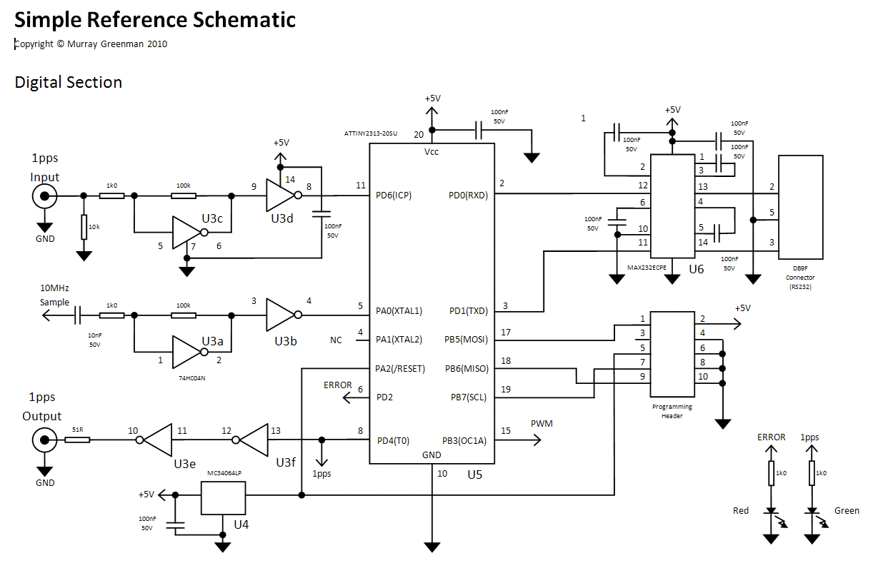
Follow the full-size Simple Reference Digital Schematic as you read this description. The 1pps reference input (from GPS receiver or other traceable source)
enters top left, and is amplified and buffered to a fast-rise square pulse by U3c and U3d. U3c is operated in a linear manner,
with a gain of 100, so can amplify signals of a few tens of millivolts. The 10k shunt resistor holds the input low when unconnected, so prevents noise upsetting the holdover capability.
If the input does not cross +2.5V however, use a series input capacitor and fit a second resistor from the input to +5V, in order to bias U3 pin 5 so the input crosses 2.5V. The 1pps pulse drives the Input Capture pin
of the micro, and is used to operate an interrupt in which the phase of a counter is sampled.
The 10MHz signal from the OCXO (10 MHz Sample) is similarly buffered by U3a and U3b to provide a fast-rise
clock to the micro at U5 pin 5. Everything in the micro other than the 1pps sample is timed from this input.
The phase detector operates in software, using a technique adapted from an an idea by Hans Summers G0UPL.
When divided by 256, the 10MHz clock generates a 39062.5Hz interrupt, which occurs as the counter in the micro
overflows. Thus when the 1pps sample point is reached, the counter has overflowed 39062.5 times, which
results in remainder values in the counter on alternate seconds that are 128 counts apart (i.e. the remainder of the count). These
consecutive readings are averaged to remove the 128 count difference and recover the mean phase in the counter.
If the OCXO is low in frequency, this mean phase will slowly reduce, and if high will increase. As the correct
frequency is approached, the phase error reduces to zero.
The control algorithm works by detecting when the phase changes by one count (100ns phase change) or more,
and uses this
information to increment or decrement the PWM demand just one step, no matter how large the phase change.
This is in effect a low-gain integrating controller, and is very immune to noise and phase jitter. An integrating
controller essentially has infinite long term gain, and operates with no error offset.
The PWM is operated by a second counter in the micro, operating in 10-bit mode. Four further bits of resolution
are achieved using dither of the least significant bit. While it would be possible to operate with higher resolution,
this was not found to
be necessary, as the finest steps are virtually lost in the noise. The PWM output is from pin 15 of U5.
A 1pps regenerated output is provided from the micro U5 pin 8, and buffered by U3f and U3e. The pulse is 50ms wide
and can be synchronized to the incoming 1pps to within 50ms. Two status outputs, ERROR and 1pps are used to
operate LEDs. The ERROR LED is illuminated when fast frequency corrections are being made (reference more
than 10ppb off frequency). The 1pps LED pulses every second, and acts as a 'power good' indicator.
Serial telemetry and input commands are operated via a 9600 bps RS232 link. U6 is the RS232 level shifter,
and also generates the necessary �9V supplies for the RS232 interface. The unit uses a DB9F connector, and
is configured as a DCE.
U4 is a reset generator for the micro, used to ensure that it resets correctly. The micro is an ATMEL
ATTiny2313 8-bit high speed RISC processor. A programming header is provided for in-circuit programming.
CONTROL TECHNIQUE
The micro controller uses three interrrupts (shown in yellow in the block diagram). Much of the important work is done
in two of these interrupts. The main timer in the micro hardware divides down from the OCXO reference
frequency, and generates an interrupt every 25.6µsec, where a software divider is operated.
The division is by 39062 or 39063 in alternate seconds, to achieve the necessary division by 39062.5; so although the real time clock keeps perfect time, there is a 25.6 microsecond p-p jitter on the seconds event and the regenerated 1pps output.
A flag is set when a new second is reached. This flag is used in the main program loop to operate a series
of one-second based routines.

Disciplined Reference Block Diagram
The other time related interrupt is generated by the reference 1pps input. During this interrupt the
value in the main divider is sampled, which gives a value proportional to the phase of the OCXO
relative to the 1pps source. When a synchronization request is provided by the user, a flag is set and this interrupt
also clears the main divider and the software divider in order to align the time to the 1pps source.
The third interrupt is driven by user commands via the serial link. The command interpreter operates
in the serial interrupt, and allows the user to set the real time clock and set the operating mode.
The main program operates by scanning for flags, and when one is encountered, a specific routine is
executed. The most important of these is the seconds flag, set whenever a new second is reached.
This operates the real time clock routine. The real time clock maintains time in BCD, seconds, minutes
and hours. The main control algorithm also operates every second, as does the 1pps pulse output and the
serial telemetry. Once all these actions have taken place, the processor goes to sleep to await the next
interrupt.
The frequency control algorithm consists of two parts. First, the integrating controller determines from the latest
phase sample and the previous phase sample whether the phase has shifted, and if so, increments or
decrements the PWM value. This value is kept as a 15-bit number, the error integrator, but only the most significant 14 bits are
used for control. This gives the routine a low gain of 50ns per second.
The phase samples are also stored every second in a FIFO
buffer, and the latest phase is compared with that 64 seconds previously. The difference represents
a frequency count with a 64 second gate time, so the micro can count the OCXO frequency with a resolution
of 1.5ppb. However, due to memory limitations, only the eight least significant bits of phase are stored, so
the technique is only valid when the phase changes less than 256 steps in this time,
i.e. when the OCXO is within about �190ppb, so is not useful within the first few minutes from startup.
Because of the 64 second delay incurred, it is also not possible to use this information for frequency control,
as stable operation would be very difficult. However, this frequency measurement is reported in the telemetry
and is used to determine when the main control gain should be increased to speed up initial settling.
When the frequency measurement indicates an error of more than 10ppb (usually soon after start-up) the gain of the
integrator is increased by a factor of four. Frequency measurement is ignored in the first minute from startup
when the data is not valid.
An estimate is made of the stability of the OCXO. This is done by counting the number of seconds which
have elapsed since the phase shifted by 100ns. The resolution of this count is four seconds, and the range
is up to 1024 seconds, i.e. a range of 4 x 10⁻⁷ to 1 x 10⁻¹⁰.
Two further flags are involved in the main routine. When the ERROR flag is detected, the ERROR LED is illuminated.
The unit is considered to be in error whenever the FAST routine is activated, i.e. when the reference is outside
the 10ppm offset limit.
When the SETUP flag is spotted, the frequency control algorithm is overridden, and instead the micro places a
left-shifted 8-bit preset value in the PWM generator. This is used during setup to trim the OCXO centre
frequency. While the
control range is quite adequate to cope with several years of OCXO ageing, the unit will
approach the correct frequency faster if the OCXO is initially (and occasionally thereafter) trimmed with care
using SETUP mode. This mode can also be used to check the control range and system gain.
COMMS PROTOCOLS
TRANSMIT (DATA)
The clock transmits time, PWM control value (feedback term), frequency offset and stability estimate every second,
starting just after the second event.
Time can be received over the serial link within 10ms of the 1pps second event. The format is
HH:MM:SS +PPpp ssFFttff<CR><LF>
HH:MM:SS is of course the time, expressed in BCD. '+' is a model identifier, used by the
PC software to determine that it has the correct hardware and a valid message to work with.
PPpp represents the PWM control value operating the OCXO frequency correction.
FFff is the measured frequency offset (1.5ppb resolution)
ss is the stability estimate.
tt is the collection of status flags.
Apart from the time (in BCD) and the flags (binary), all these values are in hexadecimal.
The unit also transmits responses to some of the time setting commands.
RECEIVE (COMMANDS)
There are no external controls on the unit. All adjustment
is achieved using the serial link to a PC. There are nine commands:
Hnn   Set hours to nn (BCD) hours
Mnn   Set minutes to nn
Snn   Set hours to nn
Dxx   Set ADJUST mode PWM to xx
+ Add one to seconds
- Subtract one from seconds
X Synchronize to 1pps second source
A Enter ADJUST mode
N Restore NORMAL mode and reset |
The commands should be used in the order shown while setting the clock. The commands shown
in red
cause the clock to stop while they are entered, and may disturb phase measurement,
so must not be used during normal operation.
Lower case letters are accepted and used as upper case. Invalid commands are ignored. The controller and clock can
be set with a simple ASCII terminal program or using the purpose-designed program 1PPS10A.
SOFTWARE
The software package is well tested, and includes both embedded code for the ATTiny2313 processor, and a
DOS PC application compatible with Windows™ XP and earlier. The package is also inexpensive
and comes with full construction and test details. See the Micro Projects page for ordering information.
Copyright � Murray Greenman 2010.
All rights reserved. Contact the author before using any of this material.